797 |
P a g e
DESIGN OF A SPEED SERIAL PERIPHERAL
INTERFACE WITH HIGH PERFORMANCE USING
WISHBONE CONTROLLER
Dhupam Koteswari
1, S. Vidyarani
2, L.Srinivas Reddy
31
M. Tech Scholar (DECS).
2Associate professor (ECE),
3Assistant. Professor (ECE)
Nalanda institute of Engineering and Technology
(NIET), Siddharth Nagar, Guntur, A.P, (India)
ABSTRACT
SPI is the serial peripheral interface protocol. Which establishes communication between the any two devices
has the capacity communicate with other devices. The device which initiates communication is called Master
and receiving device is called slave over a special network. Slave which acknowledges the response to master
over a specified network. This protocol provides communication between the various peripherals such as
controller to the memory and vice versa. This yields full duplex communication between the master and slave.
This paper provides that design of high speed serial peripheral interface. The interface facilitated with the input
and output data line as well as serial clock lines. This will supports multi slave configuration but at a time it
communicate with only one slave. This is designed in Veilog HDL.
Key Words: Master, Slave, SPI, Synchronous, CLK
I. INTRODUCTION
Nowadays each device designing with some logic control example is micro controller. The devices like LCD
drivers, RA the external devices which are operated by the controller. Every application is needed some level of
communication from the controller to peripherals. The SPI is used to communicate between the controllers to
the peripherals. In SPI we call the controller is as Master and devices called as slaves.
Serial peripheral interface is protocol which makes serial communication between the master and slaves. This
protocol is used communicate with in the chip and outside of the chip with low and medium speed applications.
It can be used for the micro controller with the external devices like EEPROM, ADC etc. This protocol used for
inter chip and intra chip communications. There are so many protocols like UART, USB, SATA used for
communication. The devices called Master and slave make use of SPI. Master device generates the clock and
this clock provides synchronization to the slave devices. This clock controls that when data has to be exchanged
and when data is valid or ready for transfer. The controlling of the clock signal done by the master device. We
can say that data exchange will happen only when there is manipulation in clock.
SPI protocols having master and slave which will perform data transfer between them.
II. WISHBONE INTERFACE
The wish bone allows you to design faster by providing a way to the problems in chip integration. Wish bone
with semiconductor IP cores. This architecture provides that more number of IP cores to be gathered to make a
system on chip architecture. This allows the wishbone to become independent of the signal levels. We already
discussed that it implements MASTER/ SLAVE model. The work organized block makes interaction with the
MASTER and makes communication. The master device made the slave device to involve in the
communication. The slaves becomes active, INTERCON is the interface which involves to store the commands
of the master and made available to the Slave.
The all wish bone signals respond with the rising edge of the clock. The clock signal of the master will make
decision on the data transfer. The master core is reset by the reset signal which is an active low. When the reset
signal is raised the registers and state machines are become preset. Whenever the master needs the service of the
host then the interrupt signal will be raised. The bus cycle working is denoted by the input cycle. The correct
data transfer is denoted by the AND function between the cycle input and the strobe input. During both inputs
are high the gate output will be high, which indicates the actual data transfer. The core is addressed by the strobe
signal. The strobe signal makes the core to respond the wishbone.
III. SPI PROTOCOL ARCHITECTURE
In the SPI we already discussed with the various registers. Here we see the architecture of them. How they
involved in communication. Those are serial peripheral control register, extension register, data register, and
status register. Transmitter data register is used to store the data before being it transmitted. It can be used for
retransmission. The receiver register is used to store the received data. Writing the data into the shift register is
accomplished by the write buffer. Reading the data from the shift register is done by the read buffer. FIFO can
be managed by the status register. To indicate the status whether it is loaded with data or else empty. Slaves are
selected by the slave select register SS by SPI controller whenever it starts communication. CTRL bit is used to
monitor the data transfer, it is set when transfer started and reset when it is completed. After completion every
If the interrupt bit in the LSB of the transmitter register is set. Then this LSB will sent over the link and it can be
kept at the LSB of the Receiver register. Similarly instead of LSB, MSB will sent over the link when this bit
become reset or clear. Mosi_pad signals are changed by falling edge of system clock when the TX_neg reg is set
otherwise they changed by the rising edge of the system clock. The mosi_pad signals will be latched by falling
edge of the system clock else they changed by the rising edge of the clock. The signal named GO busy is used to
indicate there is valid data transfer i.e. when this bit is set there is data transfer. If this bit cleared there is no
effect on it. The number of bits are being transferred is indicated by the signal CHAR_LEN.
IV. WORKING OF SPI PROTOCOL
In serial peripheral interface system clock plays a vital role. The system clock generated by the master, it will
send to each of the slave. Each of the SPI signals are synchronized with system clock. If there are more numbers
of slaves to single master. Master will use chips select signals to select the slaves. The SPI protocol data
transfers mainly depends upon the shift registers present in the Master and slave devices of units of the device.
The data transfer was controlled by the clock signal which was generated by the Master of the device. The
master when it needs transmission data will be read into its serial shift register. If slave wants transmit its data to
master it is also required to shift the data into serial shift register. When transmission required 8 clock pulses
will be generated, the data present in master shift register will be transferred to slave by MOSI line, similarly the
data present in the slave will be transmitted to the Master by the MISO line. So in this way data elements in the
shift registers were exchanged. While making communication we may use the signals as given below are SS,
MOSI, MISO, and SCK. When the master is in communication with some slave device, if it wants to control
other slave which is controlling by the some other master is not possible. In order to control that slave it has to
stop the current communication, it has to start new ommunication but we can control the multiple slaves by
using single master. This can be achieved by the time sharing between the different slaves.
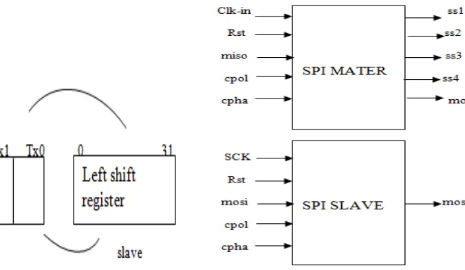
Fig 3.2 Left Shift Register Fig.No 3.3 Master And Slave Devices With Signals
4.1 SS
It refers to the slave select. Master is used to select the specified slave from the given slaves to initiate the
4.2 SCK
It refers to the serial clock. It is used to control the communication between the master and slave. It specify
instant of transfer. This synchronizes the transmission along the bus
4.3 MOSI
It serial single bit data line which makes data transfer from master to slave based on the internally shifted value
in the register
4.4 MISO
It is the serial single bit data line which makes data transfer from slave to master.
Until now we have discussed about the signals which are used to make communication. Now we will discuss
briefly about the registers which are involving to make communication as follows are data register or 8 bit shift
register, control register, baud register. We will discuss about each as follows.
Fig.No 3.4 Multi Master-Slave Configuration
4.5 Data Register Or 8 Bit Shift Register
This register forms an essential part of the SPI protocol. It will present every master and slave. Whenever data
transfer required single bit will be shifted out from the register. And same time single bit serial input from the
4.6 Control Register
This is the register which provides user control over the SPI operations. This register can be used to control the
transfer of data when it is configured properly. This register also includes enabling SPI operations, to configure
the device either as master or as slave, setting of sampling data. There are four modes of operations are provided
by SPI based on the clock phase and clock polarity.
4.7 Baud Rate Register
This register having series of divider stages. The 8 bits in the baud rate register in SPI denotes the value with
which the bus clock has to be divided. This dividers provides ample choices for end user for baud generation.
The divisors are ranging from the 2to 128. This baud rate register active only during master mode of SPI
operation.
During transmission of data by any device, the data must be read by device to making an attempt of transmitting
data. In this protocol a device will not be a simple transmitter or receiver only. The master device controls clock
signal SCK and SCK signal controls the total communication between the devices. SPI can be aptly used for the
communication between the integrated chips with low / medium speed on board devices for end user for baud
generation. The divisors are ranging from the 2to 128. This baud rate register active only during master mode of
SPI operation.
V. SIMULATION RESULTS
Here we are designing the SPI protocol which makes communication between the slow peripherals to the
controlling device which may be a master and the device which is in control is called Slave. This is designed in
VI.CONCLUSION
The Serial peripheral interface protocol is used for low speed on chip peripherals. This consist of Master and
Slave devices. The master device will use system clock to communicate with the slaves and to control them
also. This is a full duplex operation. The master will transfer the data to the slaves. The slaves will acknowledge
them according the signal given by the Master. The master will communicate at a time with only single slave.
But it supports multi slave configuration in time shared environment. In multi slave mode SS slave select signal
communicate with on chip peripherals with main device. The protocol is designed using Verilog HDL. The
same design is synthesized in Xilinx ISE 13.2 I.
REFERENCES
[1]. Design and Functional Verification of A SPI Master Slave Core Using System Verilog.
K.Aditya,M.Sivakumar, Fazal Noorbasha,T.Praveen Blessington. International Journal of Soft Computing
and Engineering (IJSCE) ISSN: 2231-2307, Volume-2, Issue-2, May 2012
[2]. Design and Implementation of a High Speed Serial Peripheral Interface Anand N, George Joseph, Suwin
Sam Oommen, and R Dhanabal School of Electronics Engineering, VIT University, Vellore, India
[3]. Frederic Leens, “An introduction to SPI and I2C protocol,” IEEE Instrumentation and Measurement
magazine, February 2009.
[4] A.K. Oudjida, M.L. Berrandjia, A. Liacha, R. Tiar, K. Tahraoui & Y.N. Alhoumays, “ Design and Test of
General-Purpose SPI Master/Slave IPs on OPB Bus,” 2010 IEEE
[5] Jianlong Zhang, Jiwei Wang, Chunyu Wu, Wenjing Zhang, “The design and realization of a comprehensive SPI interface controller,” Second International Conference on Mechanic Automation and Control
Engineering (MACE), 2011 IEEE
[6] Altera, “SPI Controller, Hard Processor System (HPS) Technical Reference Manual (TRM) V1.2,”
November 2012
[7] Lattice Semiconductor Inc., “SPI Wishbone Controller V 01.5,” January 2011.
[8] Greco M, Bussa M.P, Ferrero L, Maggiora M, Verna A, “VHDL Implementation of a SPI controller for
PANDA digital signal processing,” Nuclear Science Symposium and Medical Imaging Conference,2011
IEEE
AUTHOR DETAILS
Dhupam Koteswari, pursuing her M. Tech (DECS) from Nalanda institute of Engineering and Technology (NIET), Siddharth Nagar, Kantepudi village, Satenepalli mandal, Guntur Dist., A.P, INDIA. Her interest in digital communication concepts and is specialized in developing the communication based designs.
S.Vidyarani, has received her M.tech degree and currently working as an Associate professor (VLSI) from Nalanda institute of Engineering and Technology (NIET), Siddharth Nagar, Kantepudi village, Satenepalli mandal, Guntur Dist., A.P, INDIA. She has specialized in VLSI backend process and designing different designs in nanometre technology.
L.SRINIVAS REDDY, He completed his post graduation in DECS. His area of interest includes digital electronics, digital communication, digital system design and VLSI technology and design. His research areas are optimal communication technology. He is currently working as Asst.professor (ECE) from Nalanda institute
of Engineering and Technology (NIET), Siddharth Nagar,Kantepudi village,