International Journal of Advanced Engineering Research and Applications (IJA-ERA) ISSN: 2454-2377 Volume – 3, Issue – 5, September – 2017
Design of an FPGA-based Embedded System
for a reliable loading of multichannel data in
the on-chip memory for DSP purposes
Prof. Eng. Agostino GiorgioPolitecnico di Bari, Dipartimento di Ingegneria Elettrica e dell’Informazione, Bari, BA, Italy
E-mail Id: [email protected]
Abstract: The approach to perform Digital Signal Processing (DSP) by means of an Embedded System (ES) based on Field Programmable Gate Array (FPGA) and related Systems on Chip (SoC) is very common, useful and efficient in the electronic design practice. Moreover, one of the main problems to solve is to interface the ES with an external data source. The problem becomes further complicated for multichannel signals. To this aim, the author has designed an ES able to efficiently load into the FPGA memory data to be processed by the FPGA itself. Therefore, the aim of this paper is to describe the designed interface and its validation results. The design has been performed using the Cyclone V FPGA by Altera. The test has been performed using the evaluation board DE1-SoC by Terasic. The test bench has been developed in MATLAB environment.
Keywords: FPGA, Embedded Systems, Digital Signal Processing, MATLAB.
I. INTRODUCTION
The most recent practice in the design of Integrated Circuits (IC’s) for Digital Signal Processing (DSP) purposes, is strongly oriented towards a wide use of Programmable Logic Devices (PLD) [1], especially the Field Programmable Gate Arrays (FPGAs), and Embedded Systems (ES) designed using FPGAs [2].
In fact, an FPGA is a powerful PLD integrating combinational and sequential logic systems, memory elements, and a processor. It may be a soft or hard processor or both [3, 4].
FPGAs are characterized by a great versatility combined with a great scalability, which makes them ideal for research and prototyping purposes. In fact, unlike the Application Specific Integrated Circuits (ASICs) [5] they allow to quickly modify the designed circuit/system according to test results and can be purchased at a relatively low price. The drawback of FPGAs vs the ASICs is a quite worse performance in terms of speed and power dissipation, but the high production costs of the latter makes it preferable using the FPGA technology unless a very high rate of production is needed.
Any digital circuit can be designed by configuring the FPGA using a Hardware Description Language (HDL), for example the VerilogHDL and the VHDL [6, 7].
Moreover, the presence inside the FPGA of a number of memory mapped Input/Output (I/O) devices, i.e. chips of Random Access Memory (RAM) and registers, and the presence of a processor, allows a software to run, also. Therefore, it is possible to design a complete ES in both software and hardware part by the only FPGA chip [8].
Each FPGA factory provides also the design environment, well known as Integrated Development Environment (IDE), useful to develop digital design and to program the device. For example, the Altera factory provides the Quartus IDE [9], the Xilinix factory provides the Vivado suite [10] and so on.
International Journal of Advanced Engineering Research and Applications (IJA-ERA)
Volume – 3, Issue – 5 September – 2017
loading data coming from a multichannel signal in the on-chip memory of the FPGA. The specific device (5CSEMA5F31C6) used for the design belongs to the Cyclone V family by Altera. Anyway, the design approach is not limited to the Altera FPGA but is quite general and useful for other FPGAs families and brands.
The developed ES has a hardware and a software part and includes the Nios II soft processor embedded in the Cyclone V device where the software runs. A typical example of use is for loading and processing an Electro Cardio Graphic (ECG) signal, coming from a number of simultaneous channels ranging from 3 to 15 named derivations or leads. Therefore, data coming from the ECG signal are structured in a matrix, i.e. an array of samples for each channel [11].
Therefore, in Section II it is proposed an overview about the design environment powered by Altera. In Section III it is described the designed ES in both of them its software and hardware parts. In Section IV the test flow and results are described. Conclusions and final remarks are in Section V.
II. ALTERAQUARTUSIDE:AQUICKOVERVIEW
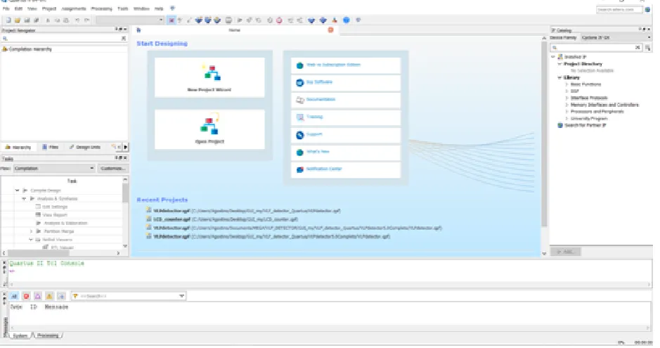
The development environment for Cyclone V FPGA used in this design is the Altera's Quartus [9]. It is a proprietary IDE software powered by the Altera Company. It provides the tools to design digital systems and embedded systems, both of them by HDL entry and by schematic entry, and allows the use of the Altera Intellectual Property (IP) for a quick and reliable implementation of very complex functions in a few steps. Moreover, Quartus includes various tools for compiling, simulating, timing and logic analysis, debugging, examining the RTL diagrams, pin assignment, device programming, and so on. Fig. 1 shows the main view of the Quartus software.
The main tools available for design purposes are the file editor both of them in the text form and in the schematic form, the Qsys and the pin planner. Moreover, the main tools available for debug purposes are the waveform editor, the timing analyzer and the logic analyzer. Finally, the programmer is the tool for programming the designed circuit into the FPGA.
International Journal of Advanced Engineering Research and Applications (IJA-ERA)
Volume – 3, Issue – 5 September – 2017
A. File editor, pin planner, waveform generator, programmer
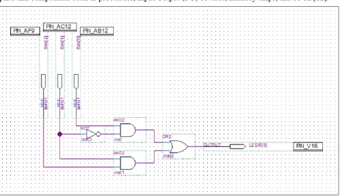
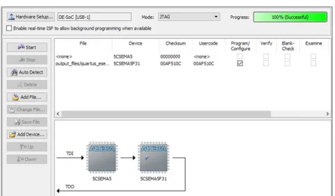
Figs. 2-4 show a typical design flow from the descriptive file creation to the FPGA programming, referring to a simple design of a xor gate using the basic and-or-not gates [1].
B. Qsys tool
The Qsys tool in Quartus IDE is necessary for the design of embedded system having many hardware parts and components such as processors, Input/Output (I/O) devices, memory chips, and so on [12].
Fig. 2. Schematic file describing a xor gate by using and-or-not gates with the proper PIN assignment made by the pin planner tool in Quartus IDE.
International Journal of Advanced Engineering Research and Applications (IJA-ERA)
Volume – 3, Issue – 5 September – 2017
Fig. 4. Programming the FPGA to act as the designed circuit, using the Programmer tool in Quartus
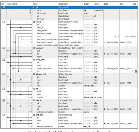
Fig. 5 shows a typical Qsys design screen, with the selected hardware parts (see the column “name”) and their connections as bold dots at the cross-points between wires (see the column “Connections”).
Fig. 5. Typical Qsys design example. Bold dots are connections. Parts under the “Name” column are hardware parts of the design
International Journal of Advanced Engineering Research and Applications (IJA-ERA)
Volume – 3, Issue – 5 September – 2017
The Qsys tool allows designing ES including either the Nios II soft processor [3], which is implemented inside the FPGA through its description in HDL code, or the hard processor, named HPS [4], also integrated on the FPGA chip and based on the Arm-Cortex architecture.
Another very useful component available in the Qsys menu is the JTAG Debug module. It allows the communication between the designed system and a host computer making also possible actions as loading a program into the on-board memory, debugging the software part of the designed ES using breakpoints arbitrarily placed at any instruction of the program, editing and reading the contents of memories and registers identified by their hexadecimal address.
A network of Avalon switch fabric called interconnection automatically generated by the Qsys tool provides the right connections between the hardware components.
The instruction memory is a Random-Access Memory (RAM) integrated into the FPGA chip.
Finally, another very useful component is the JTAG UART interface. It is useful to connect to USB-Blaster system that enables the connection between the evaluation board and a personal computer (PC). In this design, the evaluation board used is the DE1_SoC by Terasic mounting the Cyclone V 5CSEMA5F31C6 FPGA by Altera.
International Journal of Advanced Engineering Research and Applications (IJA-ERA)
Volume – 3, Issue – 5 September – 2017
C. Altera Monitor Program
Another very useful facility provided by Altera within the University Program is the “Altera Monitor Program” (AMP) [12]. This tool allows building, assembling, downloading and debugging the software part of the ES into the FPGA processor (Nios II, the soft processor, and HPS the hard processor).
Fig. 6 shows a typical view of the AMP debugging a program running on the Nios II soft processor. Further details about the AMP are in the following “Results” section.
III. DESCRIPTIONOFTHEDESIGNEDEMBEDDEDSYSTEM
The problem addressed in this paper is to perform a quick and reliable loading of data coming from a multichannel source into the FPGA I/O memory mapped devices for further processing steps. A typical example, as already stated, is the ECG signal coming from a number of channels ranging from 3 to 15.
To load such data into the SRAM memory and make them available to the FPGA for the proper processing steps, it is possible to follow a fully hardware or a mixed hardware/software approach.
A. Hardware data loading
The fully hardware approach consists in using signals of the SRAM controller properly synchronized with the clock signal driving the other parts of the circuit, and a number of digital sub-circuits, logic gates and registers, as figures 7-9 show.
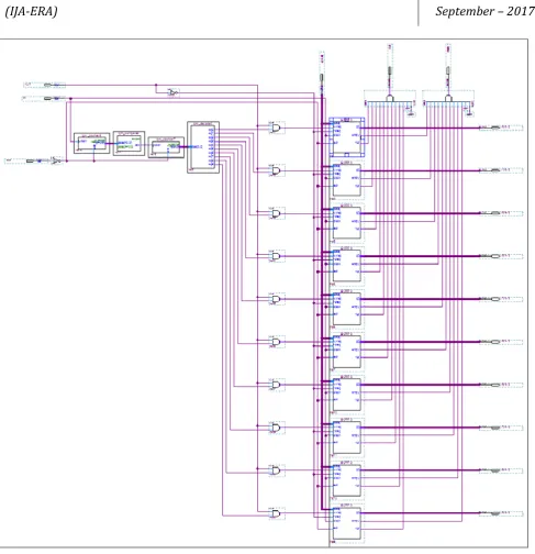
In fig. 7, there are four main blocks. The first block is clock_gen and is enabled by the signal named ck_enable. This first block generates a clock signal having the desired frequency (1 Khz in this case, i.e. the sampling frequency) starting from the main clock available in the circuit (for example a 50 Mhz clock supplied by the DE1_SoC evaluation board).
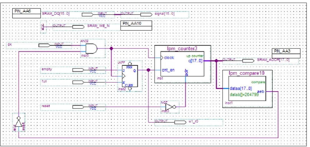
Fig. 7. Example of a circuit for the hardware data loading of a multichannel (10) signal into the on-chip memory
International Journal of Advanced Engineering Research and Applications (IJA-ERA)
Volume – 3, Issue – 5 September – 2017
drives data of all channels serially towards the block parallel. This means that data coming from all channels are sent in sequence: the first sample (16 bit) for each channel, then the second sample (16 bit) for each channel, and so on.
At this stage, the just mentioned third block parallel that receives data as serial input (16 bit per sample) conveys them in parallel multiple output, restoring the multichannel data in the right size and format and making them ready for processing.
Finally, the last block, called vlp_detection, is properly a processing section designed and implemented into the FPGA.
The signal w1_r0, coming as output from the SRAM controller, allows to enable the next step, i.e. the data processing, only if all data are loaded and ready to be processed. Fig. 8 shows the detail of the SRAM block.
Fig. 8. Detailed schematic of the SRAM block
The data flow is controlled by the flip flop JKFF, the lpm_counter3 and the lpm_compare10: lpm_counter3 increments the “SRAM_ADDR [17..0]” output every clock pulse, so the output “signal [15..0]” presents the corresponding value in the SRAM memory every clock pulse. When the empty pin is high, the JKFF enables the counter and tells the w1_r0 pin that the block is reading from the SRAM. When the full pin is high, the JKFF stops the counter and pauses the reading. The lpm_compare10 stops the data flow all data have been read. The reset pin resets the counter so the reading will restart from the beginning of the SRAM.
International Journal of Advanced Engineering Research and Applications (IJA-ERA)
Volume – 3, Issue – 5 September – 2017
Fig. 9. Detailed schematic of the block called parallel
Data to be loaded are previously stored in a .bin file and then transferred into the SRAM chip available on the evaluation board by a proper software utility developed by the author as a Graphical User Interface (GUI) in Matlab environment that will be detailed in [13].
This hardware approach is not so reliable because of the high risk of mismatching between signals and the clock running along the various parts of the circuit, due to the wide use of counters, comparators, decoders and FIFO registers to be properly synchronized. This involves considerable design difficulties and optimizations needs, and consequently high probability of fault risks. Moreover, it is very hard a deep debug of the designed system, especially to verify that data have been successfully loaded and properly structured in the output FIFOs.
B. Software/Hardware data loading: the proposed embedded system
International Journal of Advanced Engineering Research and Applications (IJA-ERA)
Volume – 3, Issue – 5 September – 2017
design an ES controlled by the Nios II processor with a fair reduction of the hardware employed. This approach significantly reduces the fault risks also making it easy a deep debug of the data loading.
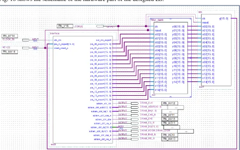
Fig. 10 shows the schematic of the hardware part of the designed ES.
Fig. 10. The embedded system designed to optimize the data loading from a multichannel source
There are two main parts in the design: the interface and the processing part. The filter bank and the vm block constitute the processing part of the ES and can change according to any processing specifications. In this paper, the processing part is purely demonstrative and designed for debug purposes only. In fact, in this paper, the focus is about the interface, which provides the data loading and reading by the FPGA for the next processing step, whatever it is.
Fig. 11 shows in detail the interface of the ES designed by the Qsys tool.
The Nios II component (in the “Description” column of fig. 11) is the soft processor available onto the FPGA chip and deals with the software task of the multichannel data loading.
The on-chip RAM is the instruction memory useful for the Nios II operations.
The JTAG UART submodule is necessary for the communication between the personal computer and the DE1_SoC evaluation board.
The SDRAM controller provides all signals necessary to manage and interface the data memory chip available on the DE1-SoC evaluation board. It has a capacity of 512 Mbits (64 Mbytes). The chip is organized into 4 banks from 8M half-word by 16 bits.
International Journal of Advanced Engineering Research and Applications (IJA-ERA)
Volume – 3, Issue – 5 September – 2017
Nios II of 3 nanoseconds. This is accomplished by using a phase-locked loop circuit (PLL).
The Parallel I/O (PIO) denominated pio_0, pio_1 and so on, up to pio_14, are the 15 registers containing the bits of the samples to be processed.
Fig. 11 (a). Embedded System design view in the Qsys tool
The PIO called out_clk provides a clock signal for the next stage of processing, so that it is synchronized with the loading of samples on the registers.
International Journal of Advanced Engineering Research and Applications (IJA-ERA)
Volume – 3, Issue – 5 September – 2017
Fig. 11 (b). Embedded System design view in the Qsys tool
The base addresses of all the memory mapped I/O devices are fixed by the designer by the Qsys to easily address them for read/write operations.
The multichannel signal used to test the loading performances of the designed system is a 15-leads ECG signal. Therefore, the first submodule of processing in fig.10 is a filter bank. It performs a band-pass filtering on the 15-leads ECG signal. The filter used is a fourth-order Butterworth type, with cut-off frequencies of 25 and 300 Hz.
The further processing submodule is called “vm” and it performs the calculation of the Vector Magnitude (VM) on the 15 leads of the ECG signal.
Both processing steps on the data loaded are performed by the FPGA.
The software part of the designed ES is written in C language and runs on the Nios II soft processor.
International Journal of Advanced Engineering Research and Applications (IJA-ERA)
Volume – 3, Issue – 5 September – 2017
Fig. 11 (c). Embedded System design view in the Qsys tool
The instruction list of the C code is:
#define PIO_BASE_00 0x4002000
#define PIO_BASE_01 0x4002010
#define PIO_BASE_02 0x4002020
#define PIO_BASE_03 0x4002030
#define PIO_BASE_04 0x4002040
#define PIO_BASE_05 0x4002050
#define PIO_BASE_06 0x4002060
#define PIO_BASE_07 0x4002070
#define PIO_BASE_08 0x4002080
#define PIO_BASE_09 0x4002090
#define PIO_BASE_10 0x40020a0
#define PIO_BASE_11 0x40020b0
#define PIO_BASE_12 0x40020c0
#define PIO_BASE_13 0x40020d0
#define PIO_BASE_14 0x40020e0
#define OUT_CLK_BASE 0x40020f0
#define SDRAM_BASE 0x0
#define SDRAM_END 0x3ffffff
#define END_WORD 0x7fff
int main (void)
{
volatile short int* pio_00_ptr = (short int*) PIO_BASE_00;
volatile short int* pio_01_ptr = (short int*) PIO_BASE_01;
International Journal of Advanced Engineering Research and Applications (IJA-ERA)
Volume – 3, Issue – 5 September – 2017
volatile short int* pio_03_ptr = (short int*) PIO_BASE_03;
volatile short int* pio_04_ptr = (short int*) PIO_BASE_04;
volatile short int* pio_05_ptr = (short int*) PIO_BASE_05;
volatile short int* pio_06_ptr = (short int*) PIO_BASE_06;
volatile short int* pio_07_ptr = (short int*) PIO_BASE_07;
volatile short int* pio_08_ptr = (short int*) PIO_BASE_08;
volatile short int* pio_09_ptr = (short int*) PIO_BASE_09;
volatile short int* pio_10_ptr = (short int*) PIO_BASE_10;
volatile short int* pio_11_ptr = (short int*) PIO_BASE_11;
volatile short int* pio_12_ptr = (short int*) PIO_BASE_12;
volatile short int* pio_13_ptr = (short int*) PIO_BASE_13;
volatile short int* pio_14_ptr = (short int*) PIO_BASE_14;
volatile short int* out_clk_ptr = (short int*) OUT_CLK_BASE;
volatile short int* sdram_ptr = (short int*) SDRAM_BASE;
volatile int delay_count;
while(*sdram_ptr != END_WORD && sdram_ptr < SDRAM_END) {
*out_clk_ptr = 0;
for(delay_count = 5000000; delay_count! = 0;
--delay_count);
*pio_00_ptr = *sdram_ptr;
sdram_ptr = sdram_ptr + 0x1;
*pio_01_ptr = *sdram_ptr;
sdram_ptr = sdram_ptr + 0x1;
*pio_02_ptr = *sdram_ptr;
sdram_ptr = sdram_ptr + 0x1;
*pio_03_ptr = *sdram_ptr;
sdram_ptr = sdram_ptr + 0x1;
*pio_04_ptr = *sdram_ptr;
sdram_ptr = sdram_ptr + 0x1;
*pio_05_ptr = *sdram_ptr;
sdram_ptr = sdram_ptr + 0x1;
*pio_06_ptr = *sdram_ptr;
sdram_ptr = sdram_ptr + 0x1;
*pio_07_ptr = *sdram_ptr;
sdram_ptr = sdram_ptr + 0x1;
*pio_08_ptr = *sdram_ptr;
sdram_ptr = sdram_ptr + 0x1;
*pio_09_ptr = *sdram_ptr;
sdram_ptr = sdram_ptr + 0x1;
*pio_10_ptr = *sdram_ptr;
sdram_ptr = sdram_ptr + 0x1;
*pio_11_ptr = *sdram_ptr;
sdram_ptr = sdram_ptr + 0x1;
*pio_12_ptr = *sdram_ptr;
sdram_ptr = sdram_ptr + 0x1;
*pio_13_ptr = *sdram_ptr;
sdram_ptr = sdram_ptr + 0x1;
*pio_14_ptr = *sdram_ptr;
sdram_ptr = sdram_ptr + 0x1;
for(delay_count = 5000000; delay_count != 0;
--delay_count);
*out_clk_ptr = 1;
for(delay_count = 10000000; delay_count != 0;
--delay_count);
International Journal of Advanced Engineering Research and Applications (IJA-ERA)
Volume – 3, Issue – 5 September – 2017
}
*pio_00_ptr = 0;
*pio_01_ptr = 0;
*pio_02_ptr = 0;
*pio_03_ptr = 0;
*pio_04_ptr = 0;
*pio_05_ptr = 0;
*pio_06_ptr = 0;
*pio_07_ptr = 0;
*pio_09_ptr = 0;
*pio_10_ptr = 0;
*pio_11_ptr = 0;
*pio_12_ptr = 0;
*pio_13_ptr = 0;
*pio_14_ptr = 0;
while(1);
}
In the first few lines of the code, there are the constant statements that indicate the base addresses of the used memory components, the SDRAM and the PIO (I/O memory mapped devices). They are the same addresses fixed by the Qsys design tool. There is also the declaration of the endword useful to end the data loading operations.
Inside the “main” function they are instantiated pointers as “short int” type to which the values of the constants defined above are assigned. These pointers allow the memory access according to the addresses they point to. The type “short int” is because of the width of both of them the SDRAM memory cells and of the PIO is 2 bytes (1 half-word). The “out_clk” signal is 1 bit wide and then still does not exceed the short int representation. The integer variable “delay_count” is also used in the delay loop: it is set as “volatile” type because otherwise the compiler eliminates the loop.
The condition of the next “while” control statement is that the loop is repeated until the pointer to the SDRAM does not reach the end-memory address, or until the variable to be pointed it is not the endword. Until the occurrence of one of these two conditions, the instructions within the loop cycle.
The loop begins by set at 0 the out_clk signal. Then it follows a delay loop to ensure that the negative clock edge reaches all the synchronous elements of the circuit. Then, the Nios II processor reads data from the SDRAM pointed cell and writes them into the first PIO. Therefore, the pointer to the SDRAM is increased by 1 in order to point to the next memory cell. These operations repeat for all 15 PIO registers.
Then, there is another delay loop to ensure the data settling in the PIO registers before the out_clk signal switches to 1, generating the rising edge of the clock signal starting the subsequent processing step.
Finally, after another delay loop terminates the main loop. The length of the delay loops was chosen to ensure that the clock driving the processing steps, i. e. the out_clock signal, has a duty cycle of about 50%.
After the end of the cycle, the PIO are reset, i.e. their content is set equal to 0. The last line contains a while loop with condition 1, meaning that the program stops on this instruction, stopping the samples loading.
This code runs on the Nios II soft processor, as already stated.
IV. RESULTS
(15-International Journal of Advanced Engineering Research and Applications (IJA-ERA)
Volume – 3, Issue – 5 September – 2017
leads) ECG signal, characterized by a 1 kHz sample rate, 16-bit resolution with 0.5 microvolts/LSB, lasting about 2 minutes. Data are firstly stored in a MATLAB matrix, called “B”, which dimensions are 115000x15. Then, it has been created a binary (B.bin) file with the B matrix using the following Matlab commands:
id = fopen('B.bin', 'w');
fwrite(id, B, 'int16');
fclose(id);
The creation of the binary file is a necessary step in order to load data in a binary format on the SDRAM chip available in the DE1_SoC evaluation board mounting the FPGA.
The loading of the B.bin file into the SDRAM, can be performed either by the Altera Monitor Program or by a loading utility developed by the author [13].
The filtering has been implemented in Matlab using the biquad function together with the filtbiq function [14]. The VM calculation has been implemented developing a user-defined Matlab function according to its definition [15].
Moreover, together with the Matlab model and the B.bin file, it has been created a project into the Altera Monitor Program (AMP) in order to program the FPGA, compile and load the C code into the instruction memory of the Nios II processor.
Creating the project in the AMP it is necessary to select the architecture Nios II. Then, choose to use a custom system by selecting the. sopcinfo and .sof files coming from the Quartus compilation of the hardware part of the designed ES (see Figs. 10-11). Then, select the program in C (or assembly if that). Finally, boot on the board, compile the program and load it into processor instruction memory.
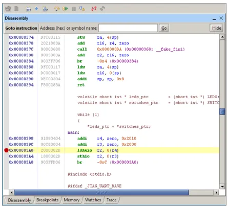
To start the debug, you can go in the disassembly screen to put the breakpoint in correspondence of the instruction 0x400145C, at the beginning of the while loop where the out_clk signal is equal to 0. The situation is as Fig. 12 shows.
Then, the binary data stored in the B.bin file are loaded into the SRAM memory by the AMP facility “Load file into memory” and then managed by the Nios II processor to make data available for the FPGA processing in the right structure.
Fig. 13 shows the debug result of the data loading into SRAM chip on the DE1_SoC evaluation board.
Any memory location (address) has its own sample value read by the AMP in the half-word (2 bytes), decimal, signed numbers format. Then, the Nios II processor loads these data into the PIO registers according to their original multichannel nature, making them available for the FPGA processing operations. To this aim, it is necessary to start the execution of the C code described above, compiled and loaded on the Nios II processor instruction memory by the AMP facilities. It is easy to verify that before starting the program, the status of the PIO registers is 0, as expected because of no data have been still loaded until the Nios II does not act, as Fig. 14 shows.
International Journal of Advanced Engineering Research and Applications (IJA-ERA)
Volume – 3, Issue – 5 September – 2017
Fig. 12. The disassembly screen of the Altera Monitor Program for a debug step-by step using breakpoints.
At this stage, it is possible to launch the program on Nios II and execute it in the “step-by step” mode for a deep debug purpose, with the “Continue” command to go from one instruction to the subsequent one. Thanks to the breakpoint set, the program stops at the beginning of each read cycle, allowing observing in the memory window the value of the samples loaded on the PIO, in correspondence of the addresses between 0x4002000 and 0x40020E0.
At the memory address 0x40020F0, the value of the out_clk signal is observable, which at the breakpoint is always 1. At the address 0x4002100, is instead observed the value of the output sample from the module that calculates the VM.
Continuing the program execution, it always stops on the same instruction allowing observing the new values loaded into the PIO and into the VM registers.
International Journal of Advanced Engineering Research and Applications (IJA-ERA)
Volume – 3, Issue – 5 September – 2017
Fig. 13. Result of the data loading by the B.bin file into on-board SRAM. Data are stored into the memory locations and are ready to be managed by the Nios II processor for the subsequent
processing steps by the FPGA:
International Journal of Advanced Engineering Research and Applications (IJA-ERA)
Volume – 3, Issue – 5 September – 2017
V. CONCLUSIONS
In this paper, it has been described an ES useful for a reliable loading of data coming from a multichannel signal into a FPGA for DSP purposes. The design has been compared with another one developed according to a fully hardware approach and it has been clearly addressed the significant reduction of fault risks following a mixed hardware/software approach, i.e. using an ES. Moreover, the design has been tested and successfully validated using the AMP. The conclusion is that the designed ES allows a reliable multichannel data loading for the FPGA processing being also the system quite simple and strongly reliable both of them in its software and hardware parts. The next step is to develop all the DSP chain in order to process the signal according to any specifications.
International Journal of Advanced Engineering Research and Applications (IJA-ERA)
Volume – 3, Issue – 5 September – 2017
Fig. 15b. Data stored into the B.bin binary data file, read in Matlab. There are exactly as in fig. 15a meaning the correct data loading operation by the Nios II processor.
Fig. 16. Vector magnitude calculated in Matlab matches enough that calculated by the FPGA processing data loaded, stored in the register which address is 0x4002100. The little mismatching is
not significant and because of different processing methods.
Conflict of interest: The author declares that he has no conflict of interest.
Ethical statement: The author declares that he has followed ethical responsibilities.
REFERENCES
[1] A. Giorgio, “Dispositivi Logici Programmabili” in Lezioni di Fondamenti di Elettronica dei Sistemi
Digitali, 1st ed, Roma Italy, Gruppo Ed. L’Espresso, 2016, pp. 251-270
[2] C. Brandolese, W. Fornaciari, “Tecnologie Hardware” in Sistemi Embedded, 1st ed., Milano Italy, Pearson
Prentice Hall, 2007, pp. 163-181
[3] Intel Corporation (February 2017), Altera, Nios II processor, Available:
https://www.altera.com/products/processors/overview.html
[4] Altera Corporation (February 2012), SoC FPGA ARM Cortex A9 MPCore Processor Advance
Information Brief. Available:
https://people.ece.cornell.edu/land/courses/ece5760/DE1_SOC/aib-01020-soc-fpga-cortex-a9-processor.pdf
[5] M. J. S. Smith, (November, 14, 2004), Addison Wesley, [online] Available:
https://archive.org/stream/ApplicationSpecificIntegratedCircuitsAddisonWesleyMichaelJohnSebastianSmit
h/Application-Specific%20Integrated%20Circuits%20-%20Addison%20Wesley%20Michael%20John%20Sebastian%20Smith#page/n0/mode/2up
[6] S. Brown, Z. Vranesic, (2009), Fundamentals of Digital Logic with VHDL Design (3rd ed.), McGrawHill,
[online] Available:
International Journal of Advanced Engineering Research and Applications (IJA-ERA)
Volume – 3, Issue – 5 September – 2017
[7] S. Palnitkar, (March, 3, 2003), Verilog HDL: A Guide to Design and Sinthesys (2nd ed.), Prentice Hall,
[online] Available the 1st ed.:
http://www.1apps.com/electronicsengg/books/Verilog%20HDL%20-%20Samir%20Palnitkar.pdf
[8] P. Marwedel, (2011), Embedded Systems Design, (1st ed.), Springer Science
[9] Altera Corporation (2016), Software Download Available:
https://www.altera.com/downloads/download-center.html
[10]Xilinix Corporation (2016), Software Download Available: https://www.xilinx.com/support/download.html
[11]A. Giorgio, “A miniaturized medical device for health monitoring and teleassistance applications”, Int. Jour. Of Bioinf. Research, vol. 4, no. 1, p. 258-262, April 2012, ISSN: 0975-3087
[12]Altera Corporation (2016), Embedded Systems Training Tutorials, Available:
https://www.altera.com/support/training/university/material_embedded_systems.html
[13]A. Giorgio, “Interfacing FPGAs with Matlab using JTAG”, unpublished
[14]The Mathworks (2017), Biquad Filter, Available:
https://it.mathworks.com/help/dsp/ref/biquadfilter.html?s_tid=srchtitle
[15]A. Giorgio, “A Model for the Real Time Detection of Ventricular Late Potentials Oriented to Embedded