ABSTRACT
SIDDALINGADEVARU, RESHMA BANGALORE. Design of a Direct Memory Access Controller for a Cortex-M0 based System on Chip. (Under the direction of Dr. W. Rhett Davis.)
The design of a Direct Memory Access Controller (DMAC) for a Cortex-M0 Processor
based System on Chip (SoC) has been illustrated in this document. The DMAC designed
in this project can handle memory to memory data transfers of multiple lengths. A
per-formance improvement of 37% was obtained when the DMAC was used to perform data
transfers. A speedup of 1.8 was observed per word transfer when the DMAC performed the
data transfer as against the CPU performing the transfer. The design was synthesized at
10 ns clock and the DMAC’s functionality was ensured with the synthesized netlist. Logic
Synthesis was carried out at Register Transfer Level at 45 nm technology with a 10 ns clock yielding a total synthesized area of 3173 um2 for the DMAC. Communication was
established between the Processor, Memory Controller and the DMAC using AHB-Lite
© Copyright 2016 by Reshma Bangalore Siddalingadevaru
Design of a Direct Memory Access Controller for a Cortex-M0 based System on Chip
by
Reshma Bangalore Siddalingadevaru
A thesis submitted to the Graduate Faculty of North Carolina State University
in partial fulfillment of the requirements for the Degree of
Master of Science
Computer Engineering
Raleigh, North Carolina
2016
APPROVED BY:
DEDICATION
BIOGRAPHY
Reshma Bangalore Siddalingadevaru was born and brought up in Bangalore, India. She
earned her Bachelor of Engineering degree in Electronics and Communication from RV
College of Engineering in 2014. She joined the Masters program in Computer Engineering
at North Carolina State University in Fall 2014. During the program, she spotted her true
interests in Digital Design and Verification. She started working on her Master’s thesis with
ACKNOWLEDGEMENTS
I would like to take this opportunity to express my gratitude towards everyone who helped
me throughout my project.
First of all, I would like to thank Dr. Rhett Davis for advising me through my thesis. His
guidance and support were invaluable in the completion of this project. I have been very
lucky to have taken two courses and a thesis under him as I have learnt a lot through the
process. I would also like to thank him for funding me in my last semester.
I would like to thank Dr. Paul Franzon for teaching ASIC Design and inspiring many
people like me to pursue a career in Digital Design. I would also like to extend my sincere
gratitude to Dr. Huiyang Zhou for teaching me Computer Architecture which is one of
the best courses I studied. I would like to thank you professors, for also serving on my
thesis committee. I would like to thank all my professors for making these two years highly
rewarding for me.
I would like to thank my friends for their inputs and support throughout the project.
Last, but not the least, I would like to thank my family for having faith in me to complete
TABLE OF CONTENTS
LIST OF TABLES . . . vii
LIST OF FIGURES. . . viii
Chapter 1 INTRODUCTION . . . 1
1.1 Motivation . . . 1
1.2 Goal . . . 2
1.3 Thesis Outline . . . 2
Chapter 2 SYSTEM OVERVIEW AND SPECIFICATION. . . 3
2.1 System Overview . . . 3
2.2 Master Interface . . . 4
2.3 Slave Interface . . . 6
2.4 System Specifications . . . 7
Chapter 3 DMAC DESIGN PROCEDURE. . . 8
3.1 DMAC Unit Overview . . . 8
3.2 DMAC Unit Modules . . . 9
3.2.1 Arbiter . . . 9
3.2.2 DMA-Slave . . . 13
3.2.3 DMA-Master . . . 14
3.3 Critical Path . . . 22
Chapter 4 STUB INTERFACE WITH THE DMAC . . . 23
4.1 Interface Procedure . . . 24
4.2 Limitation of the DRAM Controller . . . 24
4.3 Test Cases . . . 24
4.3.1 Only DMA transactions, no DRAM transactions . . . 25
4.3.2 DMA and DRAM transactions . . . 28
4.4 Synopsis . . . 33
Chapter 5 CORTEX-M0 INTERFACE AND SYNTHESIS . . . 34
Chapter 6 Conclusion . . . 44 6.1 Future Scope . . . 45
LIST OF TABLES
Table2.1 Description of Global AHB-Lite signals . . . 4
Table2.2 Description of AHB-Lite Master signals . . . 5
Table2.3 Description of AHB-Lite Slave signals . . . 7
Table3.1 Arbiter Interface . . . 12
Table3.2 DMA-Slave Interface . . . 13
Table3.3 DMA-Master Controller Interface . . . 16
LIST OF FIGURES
Figure2.1 System Overview . . . 4
Figure3.1 Detecting DMA transaction . . . 10
Figure3.2 Detecting DRAM transaction . . . 11
Figure3.3 DMA Slave Functionality . . . 14
Figure3.4 Block diagram of DMA-master . . . 15
Figure3.5 Control-path of the DMA-master . . . 17
Figure3.6 Source Address Generation . . . 18
Figure3.7 HADDR Generation . . . 19
Figure3.8 HWDATA Generation . . . 19
Figure3.9 HWRITE Generation . . . 20
Figure3.10 HTRANS Generation . . . 20
Figure4.1 Text file with only DMA transactions . . . 25
Figure4.2 Transaction dump when only DMAC transactions are issued by the AHBStub . . . 26
Figure4.3 DMA transfer starts after the DMAC registers are written to . . . 27
Figure4.4 DMA transfer mechanism . . . 28
Figure4.5 Text file with DRAM and DMA transactions . . . 29
Figure4.6 Transaction dump when both DRAM and DMAC transactions are issued . . . 30
Figure4.7 Execution of DRAM transactions before the DMA transfer . . . 31
Figure4.8 End of DMA transfer . . . 32
Figure4.9 Execution of DRAM transactions after the DMA transfer . . . 33
Figure5.1 Snippet of the C program when DMAC handles the transfer . . . 36
Figure5.2 Transaction dump of the first DMA transfer . . . 38
Figure5.3 Transaction dump of the second DMA transfer . . . 39
Figure5.4 Snippet of the C program when CPU handles the transfer . . . 41
CHAPTER
1
INTRODUCTION
1.1
Motivation
The advancements in semiconductor industry have made it possible for an entire electronic
system to fit on a single die. In this digital era of smartphones and tablets, it is necessary to
build System-on-Chips (SoC) which are powerful computers but in a very compact form.
Due to high level of integration, SoCs also reduce power consumption.
Due to the increased demand for SoC design and verification in industries, many leading
1.2. GOAL CHAPTER 1. INTRODUCTION
DMA Controller and this was the missing piece which I contributed through this project.
DMAC is one of most important components of an SoC. It bypasses the processor and
routes data directly between external interfaces and memory, thereby increasing the data
throughput of the SoC. The Central Processing Unit (CPU) initiates a DMA transfer and
continues with other operations while the transfer is in progress and receives a signal from
the DMAC when the operation is done[5]. This feature is very useful when the CPU cannot keep up with the rate of data transfer, or when the CPU needs to perform useful work while
waiting for a relatively slow I/O data transfer. The DMAC designed in this project can handle memory to memory data transfers.
1.2
Goal
The goal of this project was to design a Direct Memory Access Controller for a
Cortex-M0 Processor based SoC. The DMAC designed was capable of performing memory to
memory transfers. Various test cases were simulated to ensure successful DRAM and DMA operations. Performance analysis was done to demonstrate the efficiency of the DMAC.
The complete design was synthesized with no errors. Two AHB-Lite interconnects were
used to interface the DMAC and the DRAM controller to the processor.
1.3
Thesis Outline
The rest of this report is organized as follows. Chapter 2 discusses the AHB Lite Protocol
Interview. Chapter 3 describes the procedure to design the DMAC unit. Chapter 4 discusses the interface of AHBStub and DMAC to the DRAM Controller. Chapter 5 discusses the
interface of the Cortex-M0 processor and DMAC to the DRAM Controller and Synthesis.
CHAPTER
2
SYSTEM OVERVIEW AND SPECIFICATION
2.1
System Overview
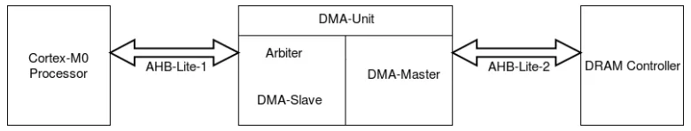
AMBA High Performance Bus(AHB) Lite protocol was used to establish communication
between the components of the SoC. It is a bus interface that supports a single master and
enables high bandwidth operation[1]. A single AHB-Lite bus was initially used, but the arbitration mechanism became very complicated as the bus allows only a single master and the CPU and the DMAC have to be the AHB-master while initiating a transaction. Another
2.2. MASTER INTERFACE CHAPTER 2. SYSTEM OVERVIEW AND SPECIFICATION
slave. In the second subsystem, DMAC is the AHB-Lite master and the DRAM Controller is
the Lite slave. For convenience, the buses of the two systems will be referred to as
AHB-Lite-1 and AHB-Lite-2 respectively. Figure 2.1 shows a block diagram of this implementation.
The DMAC has an Arbiter and a DMA-slave design which implement the slave behavior of
the DMAC. The DMA-master of the DMA-unit acts as the master to the DRAM Controller.
Figure 2.1System Overview
Table 2.1 describes the global signals in an AHB-Lite system.
Name Description
HCLK The bus clock times all bus transfers. All signal timings
are related to the rising edge of HCLK.
HRESETn The bus reset signal is active LOW and resets the system
and the bus. This is the only active LOW AHB-Lite signal.
Table 2.1Description of Global AHB-Lite signals
2.2
Master Interface
The Cortex-M0, being the bus master on AHB-Lite-1 bus, generates control signals, 32-bit
write data and address. The DMA-master does so on the AHB-Lite-2 bus. AHB master
interface signals are explained in Table 2.2. The Cortex-M0 does not generate locked
2.2. MASTER INTERFACE CHAPTER 2. SYSTEM OVERVIEW AND SPECIFICATION
additional information about bus access such as if the transfer is an opcode fetch or data
access. In this system, HPROT signal is always kept at 4’b0000. The AHB protocol supports
bursts of 4,8 and 16 beats. But the processor does not produce burst transfers and pulls the
HBURST signal to 3’b000. The HBURST signal on the AHB-Lite-2 bus is also pulled down to
3’b000 as the DRAM controller cannot handle bursts either. HTRANS indicates the type of
transfer: idle, busy, non-sequential or sequential. Only idle and non-sequential transfers are supported. The master uses an idle transfer (HTRANS=2’b00) when it does not want to perform a data transfer. Non-sequential transfer (HTRANS=2’b10) indicates a word transfer.
Name Description
HADDR[31:0] The 32-bit system address bus.
HWRITE Indicates the transfer direction. When HIGH this signal indicates a write transfer and when LOW a read transfer. It must remain constant throughout a burst transfer.
HSIZE[3:0] Indicates the size of the transfer, that is typically byte, halfword, or word.
HBURST[2:0] The burst type indicates if the transfer is a single transfer or forms part of a burst. Fixed length bursts of 4, 8 and 16 are supported. HPROT[3:0] The protection control signals provide additional information about
a bus access and are primarily intended for use by any module that wants to implement some level of protection.
HTRANS[1:0] Indicates the transfer type of the current transfer.
HMASTLOCK When HIGH, this signal indicates that the current transfer is part of a locked sequence.
HWDATA[31:0] The write data bus transfers data from the master to the slaves during write operations.
2.3. SLAVE INTERFACE CHAPTER 2. SYSTEM OVERVIEW AND SPECIFICATION
2.3
Slave Interface
The DMAC acts as a slave on the AHB-Lite-1 bus. The DRAM Controller is the slave on
the AHB-Lite-2 bus. HRDATA, HREADYOUT and HRESP are the outputs of a slave system.
Here, we do not consider HRESP and it is tied to zero. Table 2.3 explains the slave interface
2.4. SYSTEM SPECIFICATIONS CHAPTER 2. SYSTEM OVERVIEW AND SPECIFICATION
Name Description
HREADY When HIGH, the HREADY signal indicates that a transfer has finished
on the bus. This signal can be driven LOW to extend a transfer.
HRESP When LOW, the HRESP signal indicates that the transfer status is
OKAY. When HIGH, the HRESP signal indicates that the transfer status
is ERROR.
HRDATA[31:0] During read operations, the read data bus transfers data from the selected slave to the multiplexor. The multiplexor then transfers the
data to the master.
Table 2.3Description of AHB-Lite Slave signals
2.4
System Specifications
The DMAC has 3 registers - source address register, destination address register and transfer
length register. The DMAC passes on the transactions issued by the CPU to the DRAM
Controller via AHB-Lite-2 without any delay. Upon a WRITE transaction to its source address
register, the DMAC realizes that it needs to perform a transfer and issues DMA transactions
over the AHB-Lite-2 bus. Once its transfer length register is written to by the CPU, the
DMAC which behaves as the slave of AHB-Lite-1 pulls the HREADY signal LOW to stop the
CPU from issuing any more transactions till the transfer is complete. After the transfer is
complete, the DMAC continues to forward the transactions given by the CPU until the next
CHAPTER
3
DMAC DESIGN PROCEDURE
3.1
DMAC Unit Overview
DMAC is required to act as a slave in the first AHB-Lite system and as a master in the second.
Hence, there are two parts in this design - DMA-slave and DMA-master. The DMA-master
further has a Datapath which implements the DMA transfer logic and a Controller which
provides the appropriate control signals needed for the transfer. An arbiter is required to check the transactions issued by the CPU and determine if it is intended for the DRAM
controller or the DMAC. If the transaction is supposed to be given to the DRAM controller,
the arbiter passes it on to the AHB-Lite-2 bus. If it is intended for a DMA transfer, the arbiter
3.2. DMAC UNIT MODULES CHAPTER 3. DMAC DESIGN PROCEDURE
3.2
DMAC Unit Modules
The following sections discuss the functionality and implementation of the sub-modules
in the DMAC.
3.2.1
Arbiter
The arbiter module checks every transaction issued by the CPU and distinguishes between
AHB-Lite-2 and DMA-Slave intended transactions based on the address. If the transaction
is intended to be passed on to AHB-Lite-2 bus, the arbiter does so without any delay. If the
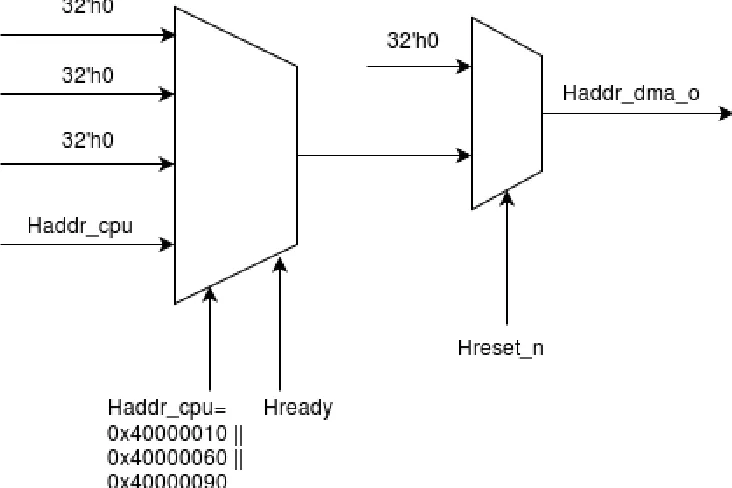
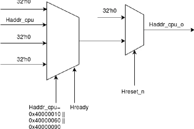
transaction is required for a DMA transfer, the arbiter directs it to the DMA Slave. Figure 3.1
represents the assignment of the input address as a DMA address upon finding the address
to be corresponding to the source, destination or the transfer_length registers of the DMAC.
Figure 3.2 shows that when the input address does not match the DMAC registers, it is passed on as an AHB-Lite-2 transaction when HREADY is HIGH. Similarly, all the other
output signals are set based on the input address value. Table 3.1 explains the signals in the
3.2. DMAC UNIT MODULES CHAPTER 3. DMAC DESIGN PROCEDURE
3.2. DMAC UNIT MODULES CHAPTER 3. DMAC DESIGN PROCEDURE
3.2. DMAC UNIT MODULES CHAPTER 3. DMAC DESIGN PROCEDURE
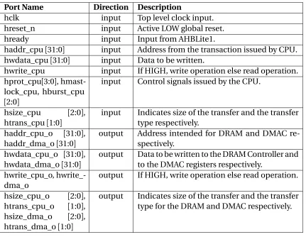
Port Name Direction Description
hclk input Top level clock input. hreset_n input Active LOW global reset. hready input Input from AHBLite1.
haddr_cpu[31:0] input Address from the transaction issued by CPU. hwdata_cpu[31:0] input Data to be written.
hwrite_cpu input If HIGH, write operation else read operation. hprot_cpu[3:0],
hmast-lock_cpu, hburst_cpu
[2:0]
input Control signals issued by the CPU.
hsize_cpu [2:0], htrans_cpu[1:0]
input Indicates size of the transfer and the transfer type respectively.
haddr_cpu_o [31:0], haddr_dma_o[31:0]
output Address intended for DRAM and DMAC re-spectively.
hwdata_cpu_o [31:0], hwdata_dma_o[31:0]
output Data to be written to the DRAM Controller and to the DMAC registers respectively.
hwrite_cpu_o, hwrite_-dma_o
output If HIGH, write operation else read operation.
hsize_cpu_o [2:0], htrans_cpu_o [1:0], hsize_dma_o [2:0], htrans_dma_o[1:0]
output Indicates size of the transfer and the transfer type for the DRAM and DMAC respectively.
3.2. DMAC UNIT MODULES CHAPTER 3. DMAC DESIGN PROCEDURE
3.2.2
DMA-Slave
Figure 3.3 shows the functionality of the DMA-slave. It latches the address obtained from
the arbiter when HREADY is HIGH. Then the address is compared with the addresses of the
DMAC registers and accordingly the source, destination and transfer_length register values
are set. It then forwards these register values to the DMA-master. The control signal
dma_-start is set to 1’b1 when the source register is written to. It can be seen that hready_pulldown is set to 1’b1 upon writing to the transfer_length register to pull the HREADY of AHB-Lite-1
LOW to stop the CPU from issuing any more transactions till the DMA transfer completes.
All the output signals are pulled LOW when the transfer is done and HREADY is restored back
for the CPU to continue giving transactions. Table 3.2 describes the DMA-Slave interface.
Port Name Direction Description
hclk input Top level clock input.
hreset_n input Active LOW global reset.
hreadyout_o output HREADY to AHB-Lite-1.
src_addr_reg,
dest_-
addr_reg,transfer_-length_reg
output DMAC registers storing source address,
des-tination address and transfer length
respec-tively.
hready_dram input HREADY of AHB-Lite-2.
hready_pulldown output Control signal to pull the HREADY of
AHB-Lite-1 LOW during DMA transfer.
dma_start output Control signal given to the DMA-master to
start the transfer.
done input Interrupt given to the CPU and DMA-slave
3.2. DMAC UNIT MODULES CHAPTER 3. DMAC DESIGN PROCEDURE
Figure 3.3DMA Slave Functionality
3.2.3
DMA-Master
Figure 3.4 shows the block diagram of the DMA-master. It includes a data-path and a
control-path and is the master of AHB-Lite-2. Inputs to the system are source address,
destination address and transfer length which are given by the DMA-slave. Source address
is the address in the memory from where the data needs to be read for the transfer to take
place. Destination address is the address in the memory to which the data needs to be
written to. Transfer length indicates the number of words to be transferred. Only word
transfers are implemented in this project as the DRAM Controller can handle only word
3.2. DMAC UNIT MODULES CHAPTER 3. DMAC DESIGN PROCEDURE
obtained by the DMA-slave, the data-path gives a DMA-start signal to the controller. Upon
receiving this signal, the control-path starts its functionality and provides the necessary
signals which control the timing of the transfer.
3.2. DMAC UNIT MODULES CHAPTER 3. DMAC DESIGN PROCEDURE
3.2.3.1 Controller
Figure 3.5 shows the state diagram of the DMA-master Controller. The 6-bit output indicated
in the state diagram is a concatenation of the control signals generated. The functionality
of these signals are explained in Table 3.3 .
Port Name Direction Description
hclk input Top level clock input.
hreset_n input Active LOW global reset.
hready_i input HREADY from AHB-Lite-2.
dma_start input Signal issued by the DMAslave at the start of
the transfer.
start output The datapath starts the transfer when start is
1.
sel_control output Signal to choose between source and
destina-tion registers during the transfer.
buf_control output Signal to control the value of HWDATA of
AHB-Lite-2.
write_control output Signal to control the value of HWRITE of AHB-Lite-2.
length_control output Signal used to increment the source and
des-tination addresses after a word transfer.
trans_control output Signal to control the value of HTRANS of AHB-Lite-2.
3.2. DMAC UNIT MODULES CHAPTER 3. DMAC DESIGN PROCEDURE
3.2.3.2 Datapath
The datapath is responsible for controlling the AHB-Lite-2 signals during the DMA transfer.
The source and destination addresses obtained from the DMA-slave need to be incremented
by 4 bytes after every word transfer. This is controlled by the length_control signal provided
by the controller. The logic for source address increment is shown in Figure 3.6.
Figure 3.6Source Address Generation
Figure 3.7 indicates the logic to write to HADDR of AHB-Lite-2. Once the addresses
for the next word transfer are ready, the datapath forwards them based on the Sel_control
signal issued by the controller. The datapath writes the chosen address to the HADDR during DMA operation. If the transaction is intended to be directly passed on to the DRAM,
the datapath does so based on the Haddr_pulldown signal obtained from the DMA-slave. It
is to be noted that only a delay of the multiplexor is added when the DRAM transactions
are passed on to the AHB-Lite-2 bus. This helps in maintaining the simulation time of the
3.2. DMAC UNIT MODULES CHAPTER 3. DMAC DESIGN PROCEDURE
Figure 3.7HADDR Generation
Figure 3.8 indicates the logic to control the HWDATA of AHB-Lite-2. Based on the
Buf_-control signal issued by the Buf_-controller and the Hready_pulldown signal by the DMA-slave,
the datapath writes the HWDATA value. During a DMA transfer, the output is the value
3.2. DMAC UNIT MODULES CHAPTER 3. DMAC DESIGN PROCEDURE
Figure 3.9HWRITE Generation
Trans_control signal issued by the controller is responsible in controlling the value of
HTRANS signal of AHB-Lite-2. Figure 3.10 indicates the logic to do the same. HTRANS was
held at 2’b10 during a transfer as only word and not burst transfers were implemented in this design. It was not possible to implement bursts due to a bug in the base testbench
used in this project. Due to this bug, during burst READ operations, the DRAM controller
read only the first data throughout the length of the burst. Hence, the DMAC was made to
perform only word transfers during both READ and WRITE transactions.
Table 3.4 explains the signals at the datapath interface.
3.2. DMAC UNIT MODULES CHAPTER 3. DMAC DESIGN PROCEDURE
Port Name Direction Description
hclk input Top level clock input.
hreset_n input Active LOW global reset.
hready_i input HREADY from AHB-Lite-2.
hrdata_i[31:0] input HRDATA from AHB-Lite-2. src_addr_reg,
dest_-addr_reg,
transfer_-length_reg
input DMAC register values storing source address,
destination address and transfer length
re-spectively obtained from DMA-slave.
dma_start input Control signal from the DMA-slave to initiate
transfer.
hready_pulldown input Control signal from the DMA-slave to choose
from the write data given by CPU or read by
the DMA-Datapath.
haddr_pulldown input Control signal from the DMA-slave to choose
from the address given by the CPU or
gener-ated by the DMA-Datapath.
haddr_o[31:0] output Address given to HADDR of AHB-Lite-2. hwdata_o[31:0] output Write Data given to HADDR of AHB-Lite-2. hwrite_o output If HIGH, write operation else read operation.
hsize_o[2:0], htrans_o
[1:0]
output Indicates size of the transfer and the transfer
type.
done output Signal which indicates the end of DMA
trans-fer.
haddr_cpu_o [31:0], hwdata_cpu_o [31:0], hwrite_cpu_o,
hsize_-input Signals obtained by the CPU generated
3.3. CRITICAL PATH CHAPTER 3. DMAC DESIGN PROCEDURE
3.3
Critical Path
The timing analysis was performed when the design was synthesized using the NanGate
45nm Open Cell Library. The critical path was identified in the datapath module and the
path was between the 2nd bit of the destination register to its 31thbit. The destination
register is updated similar to source register as shown in Figure 3.6. A schematic of this path
was observed on Design Vision and it was found to have a chain of NAND and NOT gates
which contributed to the delay. The maximum delay through this path was calculated to be
6.1815 ns. This value decided the minimum clock period required by the system. For a clock
of 10 ns, a positive slack of 3.5447 ns was observed for the system under slow operating
CHAPTER
4
STUB INTERFACE WITH THE DMAC
This chapter details the simulations used to verify the basic functionality of the DMAC.
An AHBStub was initially used as a master instead of the CPU to make the debugging of
the system easier. The DRAM transactions generated by the processor need to be passed
on to the DRAM Controller without any delay as the processor stalls issuing transactions
in case of a delay or a miss in transaction completion.The Stub was made to issue only
certain transactions which could help in understanding the DMAC’s functionality better.
An AHBStub written in System Verilog was the master on the AHB-Lite-1 bus with the
4.1. INTERFACE PROCEDURE CHAPTER 4. STUB INTERFACE WITH THE DMAC
bus.
4.1
Interface Procedure
The DMA transfer does not happen if the DRAM transactions are not handled as the CPU does not issue further data if the previous transactions are not complete. An AHBStub
was used instead of the CPU as a master which made debugging of the system easier. The
AHBStub read the transactions from a text file and passed it on to the arbiter. The arbiter
was used to decide if the transaction was intended for the DRAM or DMA based on the
address in the received transaction. The DRAM transactions are passed on to the DRAM
controller via the AHB-Lite-2 bus as long as a DMA transfer is not initiated. Once the arbiter
identifies the transactions intended for the DMA, it passes on the address, data and control
signals to the DMA slave which then sends the source, destination and transfer_length
register values to the DMA master. Once a DMA transfer is initiated, the DMA slave pulls the
HREADY of the AHB-Lite-1 bus to stop the AHBStub from issuing any more transactions. It gives the control back to the AHBStub after the DMA transfer.
4.2
Limitation of the DRAM Controller
When any program is run on the CPU, it was observed that the DRAM transaction preceeding
a WRITE to the console (address range of 0x40000000 - 0x5FFFFFFF) was not completed.
Due to this bug, a delay was added before writing to the source register of the DMAC as its
address is 0x40000010 which can cause the previous DRAM transaction to not complete.
4.3
Test Cases
The following sections describe the various test cases used to test the functionality of the
4.3. TEST CASES CHAPTER 4. STUB INTERFACE WITH THE DMAC
4.3.1
Only DMA transactions, no DRAM transactions
The first test shows a simple transfer of 8 words. Figure 4.1 shows the text file with the
transactions sent to the DMA unit. The time in Figure 4.1 indicates the time after which the
stub starts attempting to issue the transaction and not the actual time of the transaction.
Figure 4.2 shows a transaction dump of the Verilog RTL simulations and is the output of
a simple process to snoop both the AHB-Lite buses and print transactions. In Figure 4.2, the first 3 transactions were used to write values to source register, destination register
and transfer_length register of the DMAC respectively. This indicates that the DMA unit
recognizes address 0x40000010 as source register, 0x40000060 as destination register and
0x40000090 as transfer_length register. Addr_1 refers to the transactions happening between
the AHBStub and the DMA unit (via AHB-Lite-1) and addr_2 refers to the transactions
between DMA unit and the DRAM controller (via AHB-Lite-2). The following transactions
in the simulation indicate a DMA transfer of 8 bytes from source address 0x00000010 to
destination address 0x00001000. It can be seen that the first READ on the AHB-Lite-2 bus
occurs 99 cycles after the simulation leaves RESET (1015 ns) or a previous WRITE if there is
any due to the initial delay required by the DRAM Controller. Figure 4.3 shows the start of the simulation in which the registers of the DMAC are written to. Once that is done, the
datapath gives out address and write data to the AHB-Lite-2 bus starting the DMA transfer.
Figure 4.4 shows the simulation from 2005 ns where the first data is read to 2225 ns where
4.3. TEST CASES CHAPTER 4. STUB INTERFACE WITH THE DMAC
4.3. TEST CASES CHAPTER 4. STUB INTERFACE WITH THE DMAC
4.3. TEST CASES CHAPTER 4. STUB INTERFACE WITH THE DMAC
Figure 4.4DMA transfer mechanism
4.3.2
DMA and DRAM transactions
The purpose of this test was to show that DMA transfers work properly with other
trans-actions issued immediately before and afterwards, with no delay. Figure 4.5 shows the
text file with transactions to be sent to the DMAC. It has 3 DRAM transactions before the
source, destination and transfer_length registers of the DMA unit are written to. There are 3 more DRAM instructions after the DMAC registers are written to. These transactions are
expected to pass through directly to the DRAM controller via the DMA unit. Due to the
reason explained in Section 4.2, a delay has been included at the start of the WRITE to
the source register to ensure the completion of the previous DRAM transaction. Figure 4.6
shows the transaction dump corresponding to the transfers. It is observed that the first
READ on the AHB-Lite-2 bus occurs at 3155 ns which is 99 cycles after the previous WRITE
on the bus (2045 ns). It is seen that both READ and WRITE transactions intended for the
DRAM are completed without any delay. The arbiter forwards the DRAM transactions onto
4.3. TEST CASES CHAPTER 4. STUB INTERFACE WITH THE DMAC
at 3025 ns following consecutive writes to destination and transfer_length registers. This
initiates the DMA transfer of 8 bytes from source address 0x00000010 to destination address
0x00001000. The remaining 3 DRAM transactions are completed after the DMA transfer.
A delay has been added at the start of the last 3 DRAM transactions i.e., they are made to
start at 5000 ns even though the DMA transfer completes before that. The reason for this is
due to a limitation of the DMAC as it performs an extra READ transaction to the last value of source address when it is actually supposed to pass on the DRAM transaction forward.
To avoid the non-completion of the DRAM transaction following the DMA transfer, a delay
needs to be added.
4.3. TEST CASES CHAPTER 4. STUB INTERFACE WITH THE DMAC
Figure 4.6Transaction dump when both DRAM and DMAC transactions are issued
4.3. TEST CASES CHAPTER 4. STUB INTERFACE WITH THE DMAC
DMA transfer happens. At 2035 ns a READ happened from address 0x00000020 and at 2045
ns, a WRITE transaction happened to address 0x00000010. Figure 4.8 shows a part of the
DMA transfer that follows. It depicts the transfer of the last 4 words. It can be seen that the
’done’ signal of the datapath goes high after the last address is written to.
4.3. TEST CASES CHAPTER 4. STUB INTERFACE WITH THE DMAC
Figure 4.8End of DMA transfer
Figure 4.9 shows the waveform indicating the execution of the DRAM transactions after
4.4. SYNOPSIS CHAPTER 4. STUB INTERFACE WITH THE DMAC
Figure 4.9Execution of DRAM transactions after the DMA transfer
4.4
Synopsis
The DMAC was successfully interfaced with AHBStub and DRAM Controller and its
func-tionality was ensured. The DMAC could switch between DMA mode and DRAM mode
intro-CHAPTER
5
CORTEX-M0 INTERFACE AND
SYNTHESIS
This chapter details the interfacing procedure of the DMAC to the CPU and discusses the
results obtained. The Cortex-M0 processor is a very low gate count, highly energy efficient
processor that is intended for microcontroller and deeply embedded applications that
require an area optimized processor[3]. The processor’s thumb instruction set combines high code density with 32-bit performance. 2 AHB-Lite Interconnects are used for com-munication on the bus. The processor generates the transactions to be given to the DRAM
5.1. SYSTEM OVERVIEW CHAPTER 5. CORTEX-M0 INTERFACE AND SYNTHESIS
5.1
System Overview
The AHBStub which was used for debugging was replaced by the Cortex-M0 processor. It
is very important for the DMA unit to forward the transactions given by the CPU to the
DRAM without any delay as the system does not function correctly if there is any delay
or loss of transaction. The system switches to the DMA mode when the CPU writes to the
source register of the DMA unit. All transactions from the CPU are stopped till the DMA
transfer is complete by pulling the HREADY of the AHB-Lite-1 bus low. Once the transfer is
complete, the arbiter continues to forward the transactions onto the second AHB-Lite-2
bus. The input to the CPU is a C code which writes to the dedicated registers of the DMA
unit. The system can perform multiple DMA transfers as it can switch from normal mode to DMA mode whenever the source register is written to. Figure 5.1 shows the snippet of the C
program given as input to the CPU. It is seen that there are 2 DMA transfers to be performed
with a delay after each transfer. The first is a transfer of 16 words from address 0x00000040
to address 0x00004000. The second is a transfer of 8 words from address 0x00000010 to
5.2. RESULTS CHAPTER 5. CORTEX-M0 INTERFACE AND SYNTHESIS
5.2
Results
5.2.1
DMAC performing the data transfer
This test shows the operation of the DMAC when interfaced with the CPU. There are 2 DMA
transfers of length 16 and 8 which are shown here. Binary file corresponding to the program
in Figure 5.1 was loaded into the memory. It can be seen that there are "for" loops before
and after the WRITES to the DMAC registers due to reasons explained in Section 4.2 and
Section 4.3.2 respectively. These loops add delays before and after the transfer and ensure
the completion of important DRAM transactions. If the "for" loop before the WRITES to the DMAC registers is removed, the simulation stalls as the DRAM transaction needs to
be completed before the DMA transfer starts. If the last "for" loop after the second DMA
transfer is removed, both the transfers complete, however, due to non-completion of the
following DRAM transaction, the simulation stalls. The total RTL Simulation time taken
for execution was recorded to be 178495 ns. The transaction dump representing the first
transfer is shown in Figure 5.2. DMA operation starts when the length register is written
to at 11885 ns. It can be seen that until then, DRAM transactions are just being passed
through without any delay. The transfer of 16 words from address 0x00000040 to address
0x00004000 is completed at 13685 ns. The transaction dump showing the second transfer is shown in Figure 5.3. The transfer begins when the length register is written to at 14215 ns.
The transfer of 8 words from address 0x00000010 to address 0x00001000 is completed at
5.2. RESULTS CHAPTER 5. CORTEX-M0 INTERFACE AND SYNTHESIS
5.2. RESULTS CHAPTER 5. CORTEX-M0 INTERFACE AND SYNTHESIS
Figure 5.3Transaction dump of the second DMA transfer
5.2. RESULTS CHAPTER 5. CORTEX-M0 INTERFACE AND SYNTHESIS
as the master and the DRAM Controller as the slave. Upon running the code, a simulation
time of 244465 ns was noted which was 37% more than the simulation time with the DMAC
(178495 ns). With the DMAC, one set of READ and WRITE operations in a transfer took 11
cycles, which is lesser than 20 cycles which is the time taken by the CPU to do a single word
transfer. As shown in Figure 5.5, a READ from address 0x00000040 starts at 13745 ns and
the WRITE to address 0x00004000 completes at 13945 ns indicating a transfer of one word in 200 ns, i.e., 20 cycles. This accounts to a speedup of 1.8 cycles per word transfer with the
5.3. SYNTHESIS CHAPTER 5. CORTEX-M0 INTERFACE AND SYNTHESIS
Figure 5.5Transfer of one word by the CPU
5.2.3
Only DRAM transactions using DMAC
This test is to show that DRAM transactions are handled by the DMAC without any delay.
A simple fibonacci program was run on the CPU without the presence of the DMAC. The
same program was then run on the system with the DMAC. It was observed that both the
simulation times were identical. This can be further explained using Figure 3.7 where we
can see that haddr_cpu_o which is the address obtained from the transaction issued by the
CPU is passed on to the AHB-Lite-2 bus with delay corresponding only to a multiplexor.
5.3
Synthesis
The design was synthesized using Synopsys Design Compiler (45 nm technology). Clock
period was set at 10 ns. The design was latch free and devoid of major LINT errors. Setup
and hold constraints were met. The synthesizable verilog netlist of the processor, DRAM
controller and AHB-Lite were obtained from the ECE 720 curriculum. The system was
re-simulated at a gate-level with the synthesized netlists using the NanGate 45nm Open
Cell Library and DMA functionality was ensured. The behaviors of the RTL simulation and gate-level simulation were identical with the same simulation times. Area of 3173 um2 was
5.4. SUMMARY CHAPTER 5. CORTEX-M0 INTERFACE AND SYNTHESIS
5.4
Summary
The DMAC was interfaced with the CPU and multiple DMA transfers were tested. A
perfor-mance improvement of 37% was obtained when the system was simulated using the DMAC.
A speedup of 1.8 cycles was seen per word transfer when the DMAC was used for data
transfer. There was no delay while executing programs which did not need data transfers.
The only limitation in this design is the addition of delays before and after DMA transfers
CHAPTER
6
CONCLUSION
In this thesis, the design of a Direct Memory Access Controller for a Cortex-M0 based System
on Chip has been illustrated. Successful memory to memory transfers were carried out
by the DMAC for multiple transfer lengths. The DMAC was able to switch from the DMA
transfer mode to a normal DRAM operation mode if there was no signal from the CPU to
perform a transfer. A performance improvement of 37% was obtained when the system
used the DMAC to perform data transfers. A speedup of 1.8 cycles was observed per word
transfer when the DMAC performed the data transfer as against the CPU performing the
transfer. There was no delay while executing programs which did not need data transfers. The design was synthesized at 10 ns clock and the DMAC’s functionality was ensured with
the synthesized netlist.
The limitation of this design is the necessity to add delays before and after a DMA
transfer to ensure the completion of DRAM transactions issued just prior to and just after
6.1. FUTURE SCOPE CHAPTER 6. CONCLUSION
6.1
Future Scope
• Using a DRAM Controller which can handle burst data. The Synopsys DRAM
Con-troller used in the SoC cannot handle burst transactions. However, the AHB-Lite
interconnect can pass burst data. The DMAC will be more useful if burst transactions
can be handled by the DRAM Controller due to lesser overhead.
• Integrating a cache for the Cortex-M0 processor. The cache can store multiple words
and issue burst data to the AHB-Lite interconnect as the processor itself cannot issue
burst data. With these modifications, the DMAC can be further improved to handle
BIBLIOGRAPHY
[1] ARM.AMBA 3 AHB-Lite Protocol. 1.0. 2006.
[2] ARM.Cortex-M0 Devices. Generic User Guide. 2009.
[3] ARM.Cortex-M0 Technical Reference Manual. 2009.
[4] Shivashankar, K.ARM Cortex-M0 Design Start.