Available Online atwww.ijcsmc.com
International Journal of Computer Science and Mobile Computing
A Monthly Journal of Computer Science and Information Technology
ISSN 2320–088X
IJCSMC, Vol. 2, Issue. 9, September 2013, pg.268 – 278
RESEARCH ARTICLE
Power Efficient Design of
Sequential Circuits using OBSC
and RTPG Integration
Rampriya.R1, Marutharaj.T2
¹PG Scholar/ M.E VLSI Design, TKSCT, Theni, India
²Assistant Professor, Department of ECE, TKCST, Theni, India
1
[email protected]; 2 [email protected]
Abstract—In Integrated circuits a gargantuan portion of chip power is expended by clocking systems which comprises of timing elements such as flipflops, latches and clock distribution network. This paper enumerates power efficient design of shift registers using TSPC flipflops along with Clock and Power gating integration. Clock gating and power gating proves to be very effective solutions for reducing dynamic and active leakage power respectively. The two techniques are coupled in such a way that the clock gating information is used to drive the control signal of power-gating circuitry. In this paper, an activity driven fine-grained clock and power gating is proposed. First, a technique named Optimized Bus-Specific-Clock-Gating (OBSC) is introduced which reduces the problem of gated flipflop selection by appropriate selection of subset of flipflops. Then another technique named Run Time Power Gating (RTPG) is proposed for power gating the combinational logics performing redundant operations. The proposed shift registers are designed up to the layout level with 1V Power supply in 90nm technology and simulated using microwind simulations for different clock frequencies and the performance of the shift registers are evaluated by observing the average power, delay and PDP.
Keywords— Flip Flop; CMOS; TSPC; OBSC; RTPG; PDP
I. INTRODUCTION
In the past, the major concerns of CMOS VLSI designer were area, performance, cost and reliability with the power consideration of secondary importance. In recent years, designers are striving for small silicon area, low power consumption along with high speed due to ever increasing demand and popularity of portable electronics. Due to increasing use of mobile devices, consumer electronics market demand a stringent constraint on power reduction [2].
consumption occurs when the circuit has input toggles (operation mode).Leakage power dissipation occurs when the circuit doesn’t operate (Sleep mode) is referred to as standby leakage. On the other hand, leakage power consumed in operation mode is the active leakage [1].
TSPC (True Single Phase Clock) [4] technique is incorporated for designing D flipflops. TSPC uses only a single clock and two or three clocked transistors in each latch without local inversion of the clock as such inversion requires more clocked devices. Shift Registers in Digital circuits are implemented using this TSPC flipflops and their performances are simulated at different clock frequencies.
Clock gating [7-9] is the most common and widely used technique to reduce dynamic power in digital CMOS circuits. Clock gating gates the unnecessary clock toggles of a register. An activity driven optimized bus specific clock gating (OBSC) maximizes dynamic power reduction. It chooses only a subset of flip-flops (FF) to be gated selectively, and hence the problem of gated FF selection is reduced from exponential complexity into linear. After the OBSC is applied to the design, the components performing redundant operations during the clock gated period are determined. Power gating is the dominant technique to reduce standby leakage power. In order to distinguish from traditional Power gating, the power gating that minimizes active leakage power in the operation mode is referred to as Run Time Power Gating. During the clock gated period, RTPG puts the components that are performing redundant operations into sleep [10].Thus, the integration of CG and RTPG is achieved with simultaneous reduction in dynamic and active leakage power [8].
This paper is organized as follows: Section II explains the basics of TSPC D flipflop and Shift registers. Section III describes the proposed OBSC and concepts of RTPG. Section IV explains the details on how to implement PG after OBSC. Section V provides the simulation results in 90nm CMOS technology to verify the performance of the proposed circuit. Finally, conclusion is provided in section VI.
II. TSPCDFLIPFLOPSHIFTREGISTERS
A. TSPC D FLIPFLOP:
Flip-flops (FFs) are the basic storage elements used extensively in all kinds of digital designs. In particular, digital designs nowadays often adopt intensive pipelining techniques and employ many FF-rich modules. It is also estimated that the power consumption of the clock system, which consists of clock distribution networks and storage elements, is as high as 20%–45% of the total system power. Delay flipflop(DFF) forms the integral part of a digital system to construct the sequential part of the circuit to achieve low power and low area.
TSPC (True Single Phase Clock) circuit technique uses only a single clock and two to three clocked transistors. In each latch without local inversion of the clock, circuit may
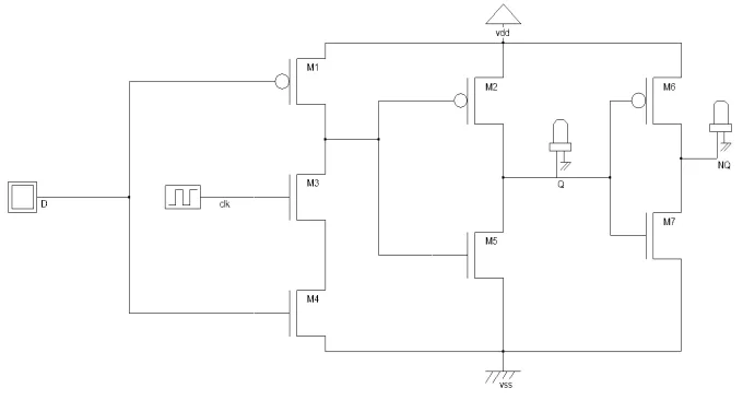
Fig . 1. Schematic of Basic TSPC D-Flip Flop
This Basic TSPC clocked latch consists of only 5 transistors such as M1,M2,M3,M4,and M5. The M3 transistor is clocked transistor. The less number of transistors in clocked latch is used to reduce total power consumption of the circuit. This clocked latch is positive edge triggered to reduce threshold voltages. In this latch the output of first stage is split [6]. The clocked transistor is less in this latch, so the power spent on the clocked node is also minimized. It has 3 NMOS transistors and 2 PMOS transistors. It is a D clocked latch D clocked latch is an opaque storage element there is no relationship between the output and present values of the input. Transistors M6 and M7 provides complemented output (NQ).
When clock is low, the input is low,M1,M5 transistors are ON. M3,M2,M4 transistors are OFF, so Q becomes ZERO and NQ becomes HIGH. When the clock is high and input is low,M1,M3,M5 transistors are ON.M2,M4 transistors are OFF, so Q becomes ZERO and NQ becomes HIGH.
When clock is low, the input is high,M2,M4 transistors are ON. M3,M1,M5 transistors are OFF, so Q becomes ZERO and NQ becomes HIGH. When the clock is high and input is HIGH,M2,M3,M4 transistors are ON.M1,M5 transistors are OFF. so Q becomes HIGH and NQ becomes ZERO. Shift Registers in Digital CMOS Circuits are implemented using this TSPC D Flipflop.
B. SHIFT REGISTERS
In digital circuits, Shift register is a group of flip-flops used to shift or transfer data from flipflop to flip-flop. It’s a group of D flip-flops connected in a chain and the clock of the flip-flops is connected in a synchronous manner. Shift register has 2 basic functions such as; data storage and data movement. Shift register has 4 classifications namely; Serial In Serial Out (SISO), Serial In Parallel Out (SIPO), Parallel In Serial Out(PISO) and Parallel In Parallel Out (PIPO) [3].
III. PROPOSED OBSC & RTPG
A. CLOCK GATING
upto 40%.Clock gating reduces the unwanted switching on the parts of clock net by disabling the clock. Clock gating can save more power by not clocking the register if there is no change in its state [8]. Hence, to reduce power consumption clock gating shuts off the clock while system maintaining its current state as shown in Fig.2
Fig . 2. Conceptual CG Architecture [8]
B. PROPOSED OBSC
Optimized Bus Specific Clock Gating is very effective technique to maximize dynamic power reduction as shown in fig.3. It chooses only a subset of flip-flops (FF) to be gated selectively, and the problem of gated FF selection is reduced from exponential complexity into linear. It works by comparing the inputs and outputs and gates the clock when they are
equal [11]. Considering N FFs in the non-CG circuit, each FF can be chosen as gated or
nongated. Hence, 2N CG solutions are possible and the exponential complexity problem is
reduced into linear. Assume that all the FFs are chosen to be gated initially, then the problem is in determining which FFs should be excluded from gating [1]. Heuristically, the FF with the maximum output data toggle rate should be excluded from gating first. This is because that maximum output data toggle rate indicates that minimum clock toggles will be gated, thus power will reduce least or even increase if the FF is gated. More formally, the FF with the maximum output toggle rate is excluded from gating first, then the FF with the second largest output toggle rate is excluded and so on until all the FFs are excluded (i.e., the original
non CG circuit). Apparently, during the process of exclusion, there will be N+1 possible CG
solutions which is linear complexity.
C.POWER GATING
As the scaling of MOS Transistor proceeds, leakage power of VLSI chips increases dramatically. Leakage power has been a major concern in portable devices because it wastes energy at standby mode and leads to shortening the battery life. One of the effective techniques to reduce stand by leakage current is power gating in which a power switch is inserted between logic circuits and the ground [8]. In the standby mode, the power switch is turned off to electrically disconnect the logic circuits from the ground, resulting in cutting off the leakage.
Power-Gating (PG) is a coarse-grained generalization of the so-called MTCMOS technique, in which a header and/or footer transistor is inserted on the up and/or pull-down network of a CMOS gate, respectively; the transistors are turned off when the gate is in stand-by mode, thus reducing the leakage current that flows in the supply-ground path as shown in Fig.4
Fig . 4. Conceptual PG Architecture [8]
D. PROPOSED RTPG
Fig 5. Basic structure for Run-time power gating [7]
IV. INTEGRATIONOF OBSC & RTPG
In order to achieve integration of CG and RTPG, apply OBSC technique to the design, then a subset of FFs is clock gated. During the clock gated period, the outputs of the gated FFs are stable. Consequently, those combinational logics whose inputs only depend on gated FF outputs will be inactive and can be power gated as shown in Fig 6.(a). For each output of the power gated cell, whether a connection to primary output presence has to be checked. A holder logic should be added in order to avoid signal floating. Suppose that four out of five FFs are clock gated. The circled cells are completely dependent on the stable gated FF outputs, so they are not active and can be power gated into sleep [1]. However, one input of
the XOR gate i is the output of ungated FF A, and one input of the AND gate h is the primary
input. Since both the ungated FF output and PI may not be stable during the clock gated
period, the XOR gate i and the AND h may be active. So they should not be power gated. In
(a) (b)
Fig 6. (a) & (b) Integration of OBSC and RTPG [1]
If RTPG has to be applied, a footer (high-Vth CMOS transistor) between the actual
ground and virtual ground of the power gated cells should be added. After the integration of CG and RTPG, the low power design should look like Fig.6 (b).The enable signal generated from OBSC is used as the sleep signal for the PG. The cells that are totally dependent on gated FF outputs are power gated. Holders are placed between the power gated cells and the non power gated cells so that the non power gated cells can function properly.
V. SIMULATION RESULTS AND DISCUSSION
The Performance of 8-bit SISO, SIPO,PISO and PIPO Shift Registers with OBSC are evaluated by considering the average power, delay and power delay product(PDP) using TSPC D Flipflop with a supply voltage of 1 V in 90nm CMOS technology. Tables 1 - 3 furnishes the performance parameters for different range of frequencies from 100MHZ – 1 GHZ
TABLEI
PERFORMANCEAT100MHZCLOCKFREQUENCY
SHIFT REGISTER
AVG POWER(µW)
DELAY (Ps)
PDP(J)
SISO 47.398 341 1.61627E-14
SIPO 47.398 48 2.27514E-15
PISO 85.404 496 4.2360E-14
TABLEII
PERFORMANCEAT500MHZCLOCKFREQUENCY
SHIFT REGISTER
AVG POWER(µW)
DELAY (Ps)
PDP(J)
SISO 58.837 165 9.708105E-15
SIPO 58.837 21 1.235577E-15
PISO 128.404 279 3.58247E-14
PIPO 38.053 51 1.940703E-15
TABLEIIII
PERFORMANCEAT1GHZCLOCKFREQUENCY
SHIFT REGISTER
AVG POWER(µW)
DELAY (Ps)
PDP(J)
SISO 69.884 98 6.8486E-15
SIPO 69.884 12 8.38608E-16
PISO 156.301 145 2.26636E-14
PIPO 51.876 33 1.711908E-15
Fig 7. Comparison of power
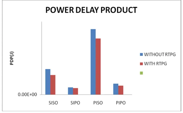
Fig 9. Comparison of power delay product(PDP)
OBSC technique reduces the power consumption to a considerable extent. In order to reduce the active leakage power encountered in digital CMOS circuits, RTPG technique is incorporated into the design by considering the shift registers with 5 TSPC D Flip Flops and their performances are evaluated at different clock frequencies. Finally, by introducing RTPG into the circuit with OBSC, a sequential circuit with integration of CG and RTPG is achieved. The proposed circuits has significant reduction in power as compared to the conventional circuits. Tables 4-5 provides performance analysis at 1 GHZ.
TABLEIV
OBSCANDWITHOUTRTPG AT1GHZCLOCKFREQUENCY
SHIFT REGISTER
AVG POWER(µW)
DELAY (Ps)
PDP(J)
SISO 115.345 137 1.58022E-14
SIPO 115.345 38 4.38311E-15
PISO 194.998 207 4.03645E-14
PIPO 78.007 86 6.708602E-15
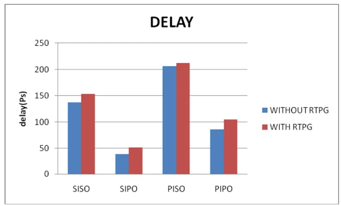
TABLEV
OBSCAND RTPG AT1GHZCLOCKFREQUENCY
SHIFT REGISTER
AVG POWER(µW)
DELAY (Ps)
PDP(J)
SISO 79.442 153 1.21546E-14
SIPO 79.442 51 4.05154E-15
PISO 162.098 213 3.45268E-14
Fig 10. Comparison of power consumption
Fig 11. Comparison of power delay product (PDP)
VI. CONCLUSION
In this Paper, a fine-grained CG and RTPG integration is achieved in sequential circuits. First, an activity driven fine-grained OBSC technique is evaluated that selects only a subset of FFs to gate . It can reduce dynamic power by 25.07%. Moreover, the clock enable signal generated in the OBSC circuit can be used as the sleep signal in RTPG. Following this, Sequential circuits that implements both OBSC and RTPG is considered and their performances are evaluated at different clock frequencies. Simulation results show that the proposed technique achieves 32% reduction in active leakage power.
REFERENCES
[1] Li Li, Ken Choi, and Haiqing Nan , “Activity-Driven Fine-grained Clock Gating and Run Time Power Gating Integration”, IEEE transactions on very large scale integration (VLSI) systems, vol. 21, no. 8, August 2013.
[2] S.M.Kang,Y.Leblebici, Ed. , “CMOS Digital Integrated Circuits analysis and design”. Third Edition, TMH, 2003
[3] M.Morris Mano,Michael D.Ciletti, , “ Digital Design”, Fourth Edition, Pearson Education Inc
[4] Christian Piguet , “Low power CMOS Circuits”, Technology, Logic Design and CAD tools,Taylor and Francis Group 2006”
[5] J.S.Wang.P.H.Yang, “A Pulse Triggered TSPC FF for High speed, Low power VLSI design Applications” IEEE, 1998
[6] Neil H.E Weste,Kamran Eshraghian, “Principles of CMOS VLSI Design,” A Systems Perspective,Second Edition,Pearson Education Inc ,2002
[7] K. Usami and N. Ohkubo, “A design approach for fine-grained run-time power gating using locally extracted sleep signals,” in Proc. Int. Conf.Comput. Design, 2006, pp. 151–161
[8] L. Bolzani, A. Calimera, A. Macii, E. Macii, and M. Poncino, “Enabling concurrent clock and power gating in an industrial design flow,” in Proc.Des. Autom. Test Eur. Conf., 2009, pp. 334–339
[9] K. Roy, S. Mukhopadkyay, and H. Mahmoodi-meimand, “Leakage current mechanisms and leakage reduction techniques in dee psubmicrometer CMOS circuits,” Proc. IEEE, vol. 91, no. 2, pp. 305–327,Feb. 2003.
[10] Y. Tsai, D. Duarte, N. Vijaykrishnan, and M. Irwin, “Characterization and modeling of run-time techniques for leakage power reduction,” IEEE Trans. Very Large Scale Integr. (VLSI) Syst., vol. 12, no. 11, pp. 1221– 1233, Nov. 2004.
[11] P. Babighian, L. Benini, and E. Macii, “A scalable algorithm for RTL insertion of gated clocks based on ODCs computation,” IEEE Trans.Comput.-Aided Design Integr. Circuits Syst., vol. 24, no. 1, pp. 29–42, Jan. 2005.
![Fig . 2. Conceptual CG Architecture [8]](https://thumb-us.123doks.com/thumbv2/123dok_us/7732176.1265936/4.612.184.426.139.272/fig-conceptual-cg-architecture.webp)
![Fig . 4. Conceptual PG Architecture [8]](https://thumb-us.123doks.com/thumbv2/123dok_us/7732176.1265936/5.612.212.406.273.480/fig-conceptual-pg-architecture.webp)
![Fig 5. Basic structure for Run-time power gating [7]](https://thumb-us.123doks.com/thumbv2/123dok_us/7732176.1265936/6.612.171.470.97.285/fig-basic-structure-run-time-power-gating.webp)
![Fig 6. (a) & (b) Integration of OBSC and RTPG [1]](https://thumb-us.123doks.com/thumbv2/123dok_us/7732176.1265936/7.612.107.543.77.351/fig-b-integration-obsc-rtpg.webp)