1
Image Generation from STL Models and its Potential Role in
Layer-Quality Evaluation for the Electron Beam Melting Process
Authors: Hay Wonga, Eric Jonesb, Peter Foxa, Chris Sutcliffea
a
School of Engineering, University of Liverpool, The Quadrangle, Brownlow Hill,
United Kingdom L69 3GH
b
Jones Consultancy, Ardlahan, Kildimo, Co. Limerick, Ireland
Corresponding author’s email: Hay Wong – [email protected]
Keywords: Additive Manufacturing; Electron Beam Melting; Electronic Imaging;
Image Generation; STL Model
Abstract
Electron Beam Melting (EBM) is an increasingly used Additive Manufacturing (AM)
technique employed by many industrial sectors, including the medical device and aerospace
industries. In EBM process monitoring, data analysis for processed layer quality evaluation is
currently focused on the extraction of information from the raw data collected in-EBM
process, i.e. thermal/ optical / electronic images, and the comparison between the collected
data and the Computed Tomography (CT)/ microscopy images generated post-EBM process.
This article postulates that a stack of bitmaps could be generated from the 3D model at a
range of Z heights during file preparation of the EBM process, and serve as a reference image
set. In-EBM process comparison between that and the workpiece images collected during the
EBM process could then be used for quality assessment purposes. In addition, despite the
extensive literature on 3D model slicing and contour generation for AM process preparation,
no methods regarding image generation from cross sections of the 3D models have been
disseminated in details. This article aims to address this by presenting a piece of 3D
model-image generation software. The software is capable of generating binary 3D model reference
images with user-defined Region-of-Interest (ROI) of the processing area, and Z heights of
the model. It is envisaged that this 3D model-reference image generation ability opens up
new opportunities in quality assessment for the in-process monitoring of the EBM process.
2
1. Introduction
This section provides the background of this study in the following order, technology gap in
STL-image generation for EBM quality evaluation, typical Additive Manufacturing (AM)
and Electron Beam Melting (EBM) build cycles, and 3D model tessellation, slicing and
G-code.
1.1 Technology Gap in STL-Image Generation for Quality Evalaiton
EBM layer-quality monitoring has been studied by various academic groups. The data
collection methods developed so far have focused on thermal / optical / electronic in-process
imaging. Regarding data analysis for the evaluation of layer-quality, Raplee et al [1]
evaluated the quality of the melting process by analysing regional slopes in pixel values of
the in-process thermal images. The relationship between temperature profile and
microstructure of components were also investigated by comparing the in-process thermal
images with post-process Electron Backscatter Diffraction (EBSD) results of EBM
manufactured components. Mireles et al [2, 3] detected intentional defects in in-process
thermal images of an EBM component via contour tracing (Moore-Neighbour tracing
algorithm). These thermal images were also correlated with post-process Computed
Tomography (CT) scan data of the EBM component to confirm the observation of the
thermal imaging system. In other articles, Mireles et al [3, 4] detected porosity in EBM
manufactured components and monitored the EBM processing area temperature via the
comparison between a calculated average pixel intensity (represents an average temperature)
from in-process thermal images and the user pre-defined pixel intensity range (represents the
desired temperature range). Rodriguez et al [5] analysed the in-process thermal images
histogram of the EBM processing area to distinguish between components with uniform
temperature and that with cold spots. Arnold et al [6] evaluated the topography and porosity
of an EBM manufactured component by comparing the in-process electronic images with
post-process CT scans and images from an optical microscope. The data analysis attempts
described so far have shown that no methodologies involve the evaluation of in-process
images against reference images generated from STL models. This article aims to fill this
knowledge gap by proposing an EBM layer-quality metric based on the use STL reference
3
Regarding the slicing of STL models and contour generation for the preparation of an AM
process, the academic communities have contributed considerably. Eragubi [7] investigated
the slicing of STL models for laser path generation, Ding et al [8] introduced the commonly
used STL slicing strategies and various types of paths in 2D path planning for AM processes,
Adnan et al [9] evaluated a line-plane analysis based STL slicing method by investigating the
layer-slicing time of STL models with a range of model complexities. Minetto et al [10]
disseminated an algorithm which makes use of arbitrary layer thicknesses to optimise STL
slicing (reduce layer thickness to reveal finer details, vice versa). Zhang et al [11] developed
an effective STL model correction and slicing algorithm to handle models with defects, such
as cracks, overlapping and non-manifold facets. Sahatoo et al [12] summarised the influences
of slicing on the AM process and components, which include, model preparation time and
surface finish. Brown et al [13] presented an algorithm for both STL slicing and G-code
generation for an entry-level 3D printer. Despite the extensive account on STL slicing, when
it comes to image generation from STL models, a detailed methodology is still yet to be
disseminated. This article aims to present the development of STL-image generation software
in details to address this knowledge gap.
1.2 Typical AM and EBM build cycles
AM, commonly referred to as 3D printing, is a manufacturing process which creates 3D
components in a layer-by-layer fashion. A typical AM cycle overview is as follow: (1) 3D
Computer-Aided Design (CAD) model creation, (2) Stereolithography (STL) file preparation,
(3) STL file slicing, and (4) the AM component building process [14]. EBM, a Powder-Bed
Fabrication (PBF) process [15], is one of the AM processes for metals. The EBM process
begins with a metal powder layer being deposited over a machine processing area. An
accelerated electron beam, serving as a thermal energy source, is used to pre-heat and sinter
the powder bed [16]. Selective melting of the design cross section contour is then carried out
and followed by hatching [17]. These steps are repeated layer-upon-layer until the
manufacture of the 3D model is complete.
1.3 3D Model Tessellation, Slicing and G-Code
3D surface geometries can be represented by triangular tessellation [14], as demonstrated by
Fig. 1. The American Standard Code for Information Interchange (ASCII) Stereolithography
4
format, each tessellation triangle is described by two pieces of information: the 3D Cartesian
coordinates of the triangle vertices, and the normal unit vector of the triangular plane
(pointing outward of the model), as summarised in Table 1 [18].
(a) Triangulation (b) Tessellation
Fig. 1 Surface triangulation and tessellation [14]
Table 1 Sample ASCII STL file format [18]
Parameter Value
Triangle Facet Normal (nx, ny, nz)
Triangle Vertices (v1x, v1y, v1z), (v2x, v2y, v2z), (v3x, v3y, v3z)
In order to prepare for a typical AM process, the STL file of a design first undergoes a slicing operation, as described by Fig. 2.
Fig. 2 STL slicing schematic. Left – 3D STL. Right – sliced STL cross sections [19]
The slice depth is set to be equivalent to the AM processing layer thickness, whilst the slice
direction is in the AM build direction. Layers of cross-sections of the original 3D design are
generated as the output. Together with the heat source (e.g. laser, electron beam) parameters,
the 2D design information is then translated into machine code, the G-code [20]. During
manufacturing, this G-code is read by the AM machine, and the AM process is carried out by
building the design cross-sections with predefined beam parameters and machine steps, in a
5
2. STL-Image Generation Software Development
The purpose of this software is to generate digial images from STL designs. The development
is partly built upon an existing Python package called “Conformal Surfaces” (University of
Liverpool, UK) [23]. Part of the “Conformal Surfaces” source code is used to enable the
import of STL files and extraction of the 3D Cartesian coordinates of triangle vertices
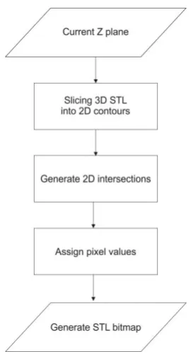
contained in the STL files. Fig. 3 uses the operation on one Z plane to give the process flow
overview of the STL-image generation software developed.
Fig. 3 STL-image generation overview, for one arbitrary Z plane
2.1 3D STL Design Slicing and 2D Contour Vector Generation
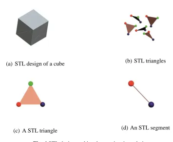
In an STL file, the surface geometry of a design is represented by a set of triangles via
6
(a) STL design of a cube (b) STL triangles
(c) A STL triangle (d) An STL segment
Fig. 4 STL design and its element in triangulation
Upon being imported to the software, the three vertices of each STL triangle are re-arranged
to represent the STL segments, and saved in the format of a list. Eq. 1 defines the three
segments in a STL triangle, whilst Table 2 summarises their respecitve compositions.
[[(𝑥1𝑆,, 𝑦1𝑆, 𝑧1𝑆), (𝑥1𝐹,, 𝑦1𝐹, 𝑧1𝐹)], [(𝑥2𝑆,, 𝑦2𝑆, 𝑧2𝑆), (𝑥2𝐹,, 𝑦2𝐹, 𝑧2𝐹)],
[(𝑥3𝑆,, 𝑦3𝑆, 𝑧3𝑆), (𝑥3𝐹,, 𝑦3𝐹, 𝑧3𝐹)] ] (1)
Where
(x1S, y1S, z1S) and (x1F, y1F, z1F) are the Cartesian coordinates of the “start” and “finish”
vertices of STL segment “1” in the 3D space. [(x1S, y1S,z1S), (x1F, y1F, z1F)] represents STL
7
Table 2 Definition of segments in a STL triangle
STL Segment Vertices Involved
[(x1S, y1S, z1S), (x1F, y1F, z1F)] (v1x, v1y, v1z), (v2x, v2y, v2z)
[(x2S, y2S, z2S), (x2F, y2F, z2F)] (v2x, v2y, v2z), (v3x, v3y, v3z)
[(x3S, y3S, z3S), (x3F, y3F, z3F)] (v3x, v3y, v3z), (v1x, v1y, v1z)
Regarding the slicing of a 3D STL design, the STL segments are analysed using vector
calculus to generate a set of 2D contours based on a set of Z planes (in typical AM processes,
the Z direction is the build direction). Fig. 5 and Eqs. 2-7 describe the working principle of
the slicing operation carried out by the software.
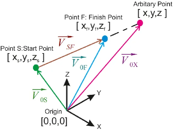
Fig. 5 Definition of a STL segment in vector calculus
𝑉𝑆𝐹
⃑⃑⃑⃑⃑⃑ =𝑉⃑⃑⃑⃑⃑⃑ − 𝑉0𝐹 ⃑⃑⃑⃑⃑⃑ 0𝑆 (2)
𝑉0𝑋
8
Where
𝑉𝑆𝐹
⃑⃑⃑⃑⃑⃑ is an arbitary STL vector segment in a 3D Cartesian space, 𝑉⃑⃑⃑⃑⃑⃑ 0𝑆 is the vector connecting
the origin and the start point S of 𝑉⃑⃑⃑⃑⃑⃑ 𝑆𝐹 , 𝑉⃑⃑⃑⃑⃑⃑ 0𝐹 is the vector connects the origin and the the finish
point F of 𝑉⃑⃑⃑⃑⃑⃑ 𝑆𝐹, and 𝑉⃑⃑⃑⃑⃑⃑ 0𝑋 is the vector connecting the origin and an arbitrary point X in space
Fig. 5, Eq. 4 and Eq. 5 show that if 𝑉⃑⃑⃑⃑⃑⃑ 𝑆𝑋 is parallel to 𝑉⃑⃑⃑⃑⃑⃑ 𝑆𝐹, then 𝑉⃑⃑⃑⃑⃑⃑ 𝑆𝑋 can be expressed by
(𝑉⃑⃑⃑⃑⃑⃑ )𝑡𝑆𝐹 , where t is a scale factor.
𝑉0𝑋
⃑⃑⃑⃑⃑⃑ =𝑉⃑⃑⃑⃑⃑⃑ +(𝑉0𝑆 ⃑⃑⃑⃑⃑⃑ )𝑡𝑆𝐹 (4)
[ 𝑥 𝑦 𝑧] = [ 𝑥𝑆 𝑦𝑆 𝑧𝑆] + [ 𝑥𝐹− 𝑥𝑆 𝑦𝐹− 𝑦𝑆
𝑧𝐹− 𝑧𝑆] 𝑡 (5)
If both the start and finish point of a chosen STL vector segment, 𝑉⃑⃑⃑⃑⃑⃑ 𝑆𝐹 , are known, it is
possible to decide if a selected Z plane intersects with the chosen STL vector segment. A
selected Z plane is defined in Eq. 6
[ 𝑥𝑃 𝑦𝑃 𝑧𝑃 ] = [ 𝑥 𝑦
𝐵] (6)
Where
𝑥𝑃 and 𝑦𝑃 are the X and Y coordinates within the selected Z plane, with values equal to any
real numbers,and 𝑧𝑃 is the Z coordinate of the selected Z plane, with a value of an arbitary
constant B
If Eq. 6 is plugged into Eq. 5, it will result in Eq.7
[ 𝑥𝑖 𝑦𝑖 𝐵] = [ 𝑥𝑆 𝑦𝑆 𝑧𝑆] + [ 𝑥𝐹− 𝑥𝑆 𝑦𝐹− 𝑦𝑆
𝑧𝐹− 𝑧𝑆] 𝑡 (7)
Where
𝑥𝑖 and 𝑦𝑖 are the X and Y coordinate of an intersection between the selected Z plane and the
9
With the coordintes of the arbitary STL segment start and finish points, and the Z coordintae
of the selected plane known, 𝑥𝑖 and 𝑦𝑖 of the intersection can be calculated through finding
the scale factor t. Fig. 3 and Eq. 7 imply that if:
1. t < 0, descpit being parallel, the intersection lies beyond the length of 𝑉⃑⃑⃑⃑⃑⃑ 𝑆𝐹
2. t = 0, the intersection is at the start point of 𝑉⃑⃑⃑⃑⃑⃑ 𝑆𝐹
3. 0 < t < 1, the intersection lies within 𝑉⃑⃑⃑⃑⃑⃑ 𝑆𝐹
4. t = 1, the intersection is at the end point of 𝑉⃑⃑⃑⃑⃑⃑ 𝑆𝐹
5. t > 1, despite being parallel in direction, the intersection lies beyond the length of 𝑉⃑⃑⃑⃑⃑⃑ 𝑆𝐹
6. t cannot be resolved, there is no intersection between the selected Z plane and the
arbitrary STL segment 𝑉⃑⃑⃑⃑⃑⃑ 𝑆𝐹
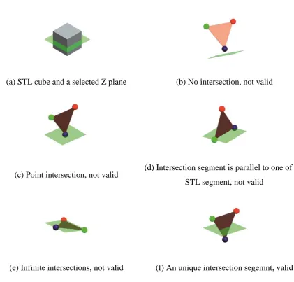
Fig. 6 illustrates all the possible outcomes between an arbitarily selected Z plane and an STL
triangle during slicing. Only Fig. 6(f) will generate a valid 2D contour ouput for further
processing in the software. A valid output is defined as an unique intersection segment made
of two unique intersections between the selected Z plane and two out of three STL segments
10
(a) STL cube and a selected Z plane (b) No intersection, not valid
(c) Point intersection, not valid (d) Intersection segment is parallel to one of the STL segment, not valid
(e) Infinite intersections, not valid (f) An unique intersection segemnt, valid
Fig. 6 STL slicing: valid and invalid outcomes
2.2 2D Intersection Generation
With regard to generating 2D intersections, virtual scan lines are overlaid on top of the 2D
contour vectors to find intersections. Fig. 7(a) depicts an arbitary cube and an arbitarily
selected Z plane. Fig. 7(b) illustrates the slicing output: 2D contour vectors which live on the
selected Z plane, and Fig. 7(c) demonstrates how intersections with virtual horizontal scan
lines are defined. Based on the definition given in Fig. 5 and Eq. 4, the interesctions between
the 2D contour vectors and the virtual scan lines can be found by applying Eq. 8, which is a
2D version of Eq.4. Table 3 summarises the various outcomes in the interactions between
virtual scan lines and the 2D contour vectors. Only the outcome which results in an even
11
(a) STL cube and a selected Z plane (b) 2D contour vectors
(c) Virtual horizontal scan lines, 2D contours and intersections
Fig. 7 2D intersections generation
𝑉0𝑋
⃑⃑⃑⃑⃑⃑ =𝑉⃑⃑⃑⃑⃑⃑ +(𝑉0𝑆 ⃑⃑⃑⃑⃑⃑ )𝑡𝑆𝐹
[𝑥𝐶 ] = [𝑛 𝑥𝑦𝑆
𝑆] + [
𝑥𝐹− 𝑥𝑆
𝑦𝐹− 𝑦𝑆] 𝑡 (8)
Where
C is the known Y location of a scan line, and 𝑥𝑛 , is the X coordinate of an intersection
12
Table 3 Intersections between virtual scan lines and 2D contour vectors
Scenario Description Write to output?
Total number of intersection is an even
number, intersections lie within vectors Yes
Intersections lie beyond vectors No
Total number of intersection is an odd
number No
One of the intersections is at the start/
finish point of one of the vectors No
One of the vectors is running parallel
to the virtual scan line No
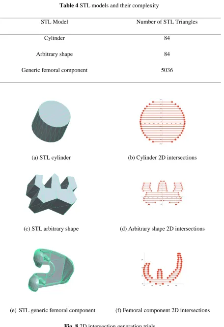
Three trials were conducted with different STL designs to verify the operation of slicing and
2D intersection generation. These designs were created in the Creo software (PTC, USA) and
saved as STL files. Table 4 summarises the STL files complexities whilst Fig. 8 shows the
13
Table 4 STL models and their complexity
STL Model Number of STL Triangles
Cylinder 84
Arbitrary shape 84
Generic femoral component 5036
(a) STL cylinder (b) Cylinder 2D intersections
(c) STL arbitrary shape (d) Arbitrary shape 2D intersections
(e) STL generic femoral component (f) Femoral component 2D intersections
14 2.3 Pixel Value Assignment
With regard to pixel value assigment, the 2D intersections on each virtual horizontal scan line
are analysed, as described by process flow chart in Fig. 9 (an elaboration of the overview
given in Fig. 3). The key factor is to only keep the scan lines with an even number of
intersections, and discard the rest of the scan lines. Figs. 10 (a) and (b) illustrate this idea with
a set of 2D contour vectors of a STL cube. Pixels which lie between the 2D intersections are
assigned the colour white, whilst others are assigned the colour black. The location, length
and number of the virtual scan lines define the output 2D bitmap size (number of image pixel
columns and rows).
15
(a) 2D intersections (b) Resultant binary bitmap
Fig. 10 Pixel assignment demonstration
3. Results [500]
3.1 Image Generation from STL Design
Four STL designs, as summarised in Table 5, were downloaded from the free online STL
database, Thingiverse (https://www.thingiverse.com/). The designs were imported into the
Magics software (Materialise NV, Belgium) for re-scaling to fit into a 200mm x 200mm
Region of Interest (ROI), and to align the design frontal plane direction with the origin Z axis
in the software. These STL designs were then imported to the image generation software for
16
Table 5 STL models and their complexity
STL Model Total Number of STL Triangles
Model Z
Height (mm)
Average STL Triangles to
Slice Through (mm-1)
1 x Hulkbuster 20606 62.7 329
9 x Generic femoral
component 45414 69 658
1 x St. Basil 77666 99.8 778
17
(a) Hulkbuster STL design (b) Image generation ROI
(c) 2001x2001pixel, Z=41mm (d) 2001x2001pixel, Z=52mm
18
(a) Generic femoral components STL design (b) Image generation ROI
(d) 2001x2001pixel, Z=7mm (d) 2001x2001pixel, Z=17mm
19
(a) St. Basil STL design (b) Image generation ROI
(c) 2001x2001pixel, Z=13mm (d) 2001x2001pixel, Z=53mm
20
(a) T-Rex STL design (b) Image generation ROI
(c) 2001x2001pixel, Z=30mm (d) 2001x2001pixel, Z=36mm
Fig. 14 T-Rex skeleton STL-image generation (slicing along Z direction)
Table 6 summarises the STL-image generation time. In general, the time is proportional to
the complexity of the STL model, i.e. the average number of STL triangle to slice through in
the Z height. Nevertheless, the design of the model is thought to have an impact on the image
generation time as well. With an average of 658 mm-1 STL triangles to go through in the Z
height, the software took an average of 7.67s to generate one image from the 9 x generic
femoral component, whilst the software only took 5.09s to generate an image from the 1 x St.
21
demonstrates that, apart from the sheer number of STL triangles to go through per Z height,
their arrangement in space (how intricate the design is) is thought to also influence the image
generation time.
Table 6 STL-image generation time. Data rounded to 3.s.f.
Model Average STL Triangles to Slice Through (mm-1)
Total Image Generated Total Time (s) Average Image Time (s)
1 x Hulkbuster 329 59.0 269 4.56
9 x Generic
femoral
component
658 66.0 506 7.67
1 x St. Basil 778 193 982 5.09
1 x T-Rex 14400 11.0 662 60.2
3.2 Demonstration: Post-EBM Process Electronic and STL Images Generations
This section demonstrates the results of the STL-image generation software when it was used
alongside a custom digital electronic imaging system prototype developed for an Arcam A1
EBM machine (Arcam AB/ GE Additive, USA) [24]. Fig. 15(a) is the schematic of the
prototype. The prototype consisted of a feedback electron sensor (modified Arcam
heat-shield frame and plates), a data logger (Arduino DUE microcontroller break-out board),
signal amplifier and electronic image generation software. The prototype was designed to
generate digital electronic images from the secondary electrons and backscattered electrons,
originating from the interactions between the machine’s primary electron beam and the
processing area. Fig. 15(b) shows the imaging target [24] used in this demonstration. The
target was manufactured by the EBM machine, made of Ti-6Al-4V alloy, and designed to
consist of nine solidified / sintered powder regions. Upon completion, the target was taken
out of the EBM machine for excess powder removal in a Powder Recovery System (PRS)
(Arcam AB/ GE Additive, USA). In this demonstration, after the removal of excess powder,
22
Digital electronic images were generated with the ROI of location “6” from the surface of the
target, at room temperature.
(a) Schematic of the prototype (b) Imaging target
Fig. 15 Electronic imaging system prototype and the imaging target [24]
Raw digital electronic images were generated from location “6” of the imaging target, as
illustrated by Figs. 16(a) and (c). In order to generate binary electronic images, image
processing was carried out before image thresholding. Noise was removed by applying a
median filter, and image contrast was enhanced by carrying out histogram equalisation with
the use of the FIJI software (same as ImageJ, open source). Eq. 9 [25] and Eq. 10 [25] define
the median filter and histogram equalisation functions used respectively. The median filter
applied had a user-defined neighbourhood area of a circle with radius of two pixels. The
histogram equalisation was carried out with a user-defined saturated pixel value of 0.3%,
allowing 0.3% of the total pixels to become saturated.
𝑓̂(𝑥, 𝑦) =(𝑠,𝑡)∈𝑆𝑚𝑒𝑑𝑖𝑎𝑛𝑥𝑦 {𝑔(𝑠, 𝑡)} (9)
23
𝑓̂ (x,y) is the pixel-value of the filtered image at (x,y), g(s,t) is the pixel-value of the raw
image at (s,t), and Sxy represents the set of coordinates within a user-defined area of an
image.
𝑦𝑘 ≜ ⌊[(𝐿 − 1) ∑ ℎ(𝑖)
𝑘
𝑖=0
] + 0.5⌋ 𝑘 = 0, 1, 2, … . . , 𝐿 − 1 (10)
Where
L is the bit-depth in an image, k is the pixel-value within the bit-depth, L, h(i) is the
normalised histogram which gives the probability of occurrence of pixel-value, I, ∑𝑘𝑖=0ℎ(𝑖)
is the cumulative probability distribution of the normalised histogram, and yk is an integer,
the equalised number of pixel with a pixel-value of k.
Figs. 16(d) and (e) show the processed and binarised electronic images of location “6”
respectively. Binary images with the same ROI (location “6”) were also generated from the
24
(a) Screenshots from the Build Assembler
software (Arcam AB)-electronic image ROI (b) STL-image ROI
(c) Raw electronic image (d) Processed electronic image
(e) Binary electronic image (f) STL-image
25
4. Discussion
Discussion on image generation results will be presented in the following order: image
generation from STL designs, and reference image generation.
4.1 Image Generation from STL Design
Table 5 and Figs. 11-14 show that the STL-image generation software is capable of handling
STL files with different level of complexities: from 20606 to 887500 number of STL
triangles. In addition, Figs. 11-14 verify that the software is capable of generating images at
various Z heights, and the pixel values are correctly allocated to represent the interior and
exterior of the STL models in the bitmaps. It is thought that the ability to generate bitmaps
representing the 2D cross sections of STL designs at various Z heights is an important step
for EBM process monitoring. These bitmaps have the potential to be used as reference
images in layer-quality assessment, and will be discussed in Section 4.2.
4.2 Demonstration: Post-EBM Process Electronic and STL Images Generations
Fig. 16(b) and (f) verify that the STL-image generation software has the flexibility to allow
users to define the image FOV by selecting specific ROI on the imaging target. It is thought
that these STL images, i.e. Fig. 16(f), can serve as “reference images” whilst the electronic
images, i.e. Fig. 16(e) (with the same Z height and ROI as Fig. 16(f)), from the prototype as
“workpiece images”. The comparison between these reference and workpiece images is
thought to have the potential to reveal typical EBM process issues which include, but not
limited to, poor powder bed deposition [26] and peel-off metallisation fallen onto the
processing area [27]. These reference and workpiece image sets generated from the
STL-image generation software and the custom electronic imaging system prototype are thought to
open up opportunities for the development of a layer-quality measure for the EBM process.
Fig. 17 illustrates this concept. Although, in this study, the workpiece electronic image, Fig.
16(e), was generated post-EBM process, this demonstration is thought to have showcased the
potential for image-image comparison to be conducted in-process for the evaluation of the
EBM layer quality on-the-fly. With this EBM process monitoring concept, potential metrics
could be developed as outlined below: (1) a deviation image could be generated for each
EBM layer to reveal the differences in pixel values between a reference and workpiece image
26
from a stack of deviation images generated throughout the EBM process. This model could
serve as an overall, quantitative feedback to the users on the EBM build quality. Despite the
possibilities suggested by the results and concepts derived from this study, Table 6 shows that
the minimum reference image generation time was 4.56s whilst the maximum was 60.2s in
this study. Although it is expected that the whole reference image set would be generated
before the actual EBM process begins, further development is needed to improve the image
generation software to reduce the image generation time, in order to minimise the extra time
incurred in EBM build preparation due to the generation of a reference image set used for
quality monitoring purposes.
Fig. 17 Multi-layer monitoring and analysis
5. Conclusions
In order to address the current knowledge gap and contributing to the field of AM / EBM
process monitoring, a method of bitmap generation from STL models has been disseminated
in this article. The development of a piece of STL-image generation software has been
presented in details. The software has demonstrated the ability to generate binary STL
reference images from user-define ROIs of the processing area and Z heights of STL models
with various complexities. Moreover, the concept of an EBM layer quality assessment metric
based on this STL-image generation software and the use of a custom electronic imaging
system prototype has been proposed. This reference/ workpiece image sets comparison metric
layer-by-27
layer fashion. There will, however, be challenges ahead in order to realise this potential.
Future studies will need to focus on, firstly, improving the image generation algorithm to
reduce the image generation time. In this study, the minimum and maximum times recorded
to produce a reference image from STL models were 4.56s and 60.2s respectively. At these
rates, the extra time incurred to the EBM build preparation stage due to the generation of a
full stack of reference images from the whole STL model is expected to be too long to make
this metric practical. Secondly, in order to further assess the applicability of this image
comparison metric, the custom electronic imaging system prototype needs to carry out
in-process data collection in a real EBM build to generate electronic images on-the-fly.
Image-image comparison between a pair of STL reference Image-image and workpiece electronic Image-image
needs to be conducted in real-time, after the processing of each EBM layer, during a real
EBM build.
Acknowledgements
The Author(s) declare(s) that there is no conflict of interest. This research received no
specific grant from any funding agency in the public, commercial, or not-for-profit sectors.
The EBAM machine was purchased, in part from a grant received for the EPSRC Centre for
Innovative Manufacturing in Additive Manufacturing.
6. References
1.
J. Raplee, M. M. Kirka, R. Dinwiddie, A. Okello, R. R. Dehoff , S. S. Babu, A. Plotkowski(2017) Thermographic microstructure monitoring in electron beam additive manufacturing.
Scientific Reports, 7:43554, 2017. DOI: 10.1038/srep43554.
2. J. Mireles, P. Morton, A. Hinojos, R.B. Wicker, S. Ridwan (2015) Analysis and correction
of defects within parts fabricated using powder bed fusion technology. Surf. Topogr.: Metrol.
Prop., 3, 2015. DOI: 10.1088/2051-672X/3/3/034002.
3. J. Mireles, S.M. Gaytan, D. Espalin, R.B Wicker, S. Ridwan (2014) Automatic layerwise
acquisition of thermal and geometric data of the electron beam melting process using infrared
28
4. J. Mireles, S.M. Gaytan, D.A. Roberson, R.B. Wicker, C. Terrazas (2015) Closed-loop
automatic feedback control in electron beam melting. Surf. Topogr.: Metrol. Prop.,78:1193–
1199, 2015. DOI: 10.1007/s00170-014-6708-4.
5. E. Rodriguez, D. Espalin, C. Terrazas, D. Muse, C. Henry, E. MacDonald, R.B. Wicker, F.
Medina (2012) Integration of a thermal imaging feedback control system in electron beam
melting. In Proceedings of the Solid Freeform Fabrication Symposium, 2012.
6. C. Arnold, C. Pobel, F. Osmanlic, C. Körner (2018) Layerwise monitoring of electron
beam melting via backscatter electron detection. Rapid Prototyping Journal 24/8 (2018)
1401–1406. DOI 10.1108/RPJ-02-2018-0034
7. M. Eragubi (2013) Slicing 3D CAD Model in STL Format and Laser Path Generation.
International Journal of Innovation, Management and Technology, Vol. 4, No. 4,
DOI: 10.7763/IJIMT.2013.V4.431
8.
D. Ding, Z. Pan, D. Cuiuri, H.Li, S. van Duin (2016) Advanced Design for AdditiveManufacturing: 3D Slicing and 2D Path Planning . http://dx.doi.org/10.5772/63042
9. F. Adnan, F. Romlay, M. Shafiq (2018) Real-time slicing algorithm for Stereolithography
(STL) CAD model applied in additive manufacturing industry. iCITES, 2018, IOP Conf.
Series: Materials Science and Engineering 342 (2018) 012016.
doi:10.1088/1757-899X/342/1/012016
10. R. Minetto, N. Volpato, J. Stolfi, M. R. Gregori, M. da Silva (2017) An Optimal
Algorithm for 3D Triangle Mesh Slicing. Computer-Aided Design. Computer-Aided Design
Volume 92, November 2017, Pages 1-10. https://doi.org/10.1016/j.cad.2017.07.001
11. L. Zhang, M. Han, S.Huang (2002) An Effective Error-Tolerance Slicing Algorithm for
STL Files. Int J Adv Manuf Technol (2002) 20:363–367
https://link.springer.com/article/10.1007/s001700200164
12. Divesh R. Sahatoo, B. Chowdary, F. Ali, R. Bhatti (2008) Proceedings of The 2008
IAJC-IJME International Conference ISBN 978-1-60643-379-9.
29
13. A. Brown, D. de Beer (2013) Development of a stereolithography (STL) slicing and
G-code generation algorithm for an entry level 3-D printer. 2013 Africon, Pointe-Aux-Piments,
2013, pp. 1-5. doi: 10.1109/AFRCON.2013.6757836
14. J.O. Milewski (2017) Additive Manufacturing of Metals: From Fundamental Technology
to Rocket Nozzles, Medical Implants, and Custom Jewelry, pages 99–116. Springer, London.
15. B. Gustavsson (2018) Effect of beam scan length on microstructure characteristics of
EBM manufactured alloy 718. Master’s thesis, KTH Royal Institute of Technology in
Stockholm
16. C. Körner (2016) Additive manufacturing of metallic components by selective electron
beam melting — a review. International Materials Reviews, 61:361–377, 2016.
DOI: https://doi.org/10.1080/09506608.2016.1176289.
17. C.J. Smith, E.H. Nava, M. Thomas, S. Tammas-Williams, S. Gulizia, D. Fraser, I. Todd,
F. Derguti (2015) Dimensional accuracy of electron beam melting (EBM)
additivemanufacture with regard to weight optimized truss structures. Journal of Materials
Processing Technology, 229:128–138, 2015.
18. D. Touretzky (2016) STL files and slicing software. Teaching Materials. 15-294-A4
Rapid Prototyping Technologies Spring, Computer Science Carnegie Mellon University.
https://www.cs.cmu.edu/afs/cs/academic/class/15294u-s16/
19. Y. Tascıoglu O. Topcu and H. O. Unver (2011) A method for slicing CAD models in
binary STL format. In Proceedings of the 6th International Advanced Technologies
Symposium(IATS’11),May2011.https://pdfs.semanticscholar.org/87de/4bb53e7551cda6af80
71189ca62b57a7b0da.pdf
20. Y. Kanada (2016) Method for procedural 3D printing using a Python library. Journal of
Information Processing, 24:908–916, 2016. DOI: 10.2197/ipsjjip.24.908.
21. G. Franchin, M. Kayser, C. Inamura, S. Dave, J.C. Weaver, P. Houk, P. Colombo, M.
30
glass. 3D PRINTING AND ADDITIVE MANUFACTURING, 2:92–105, 2015.
DOI: 10.1089/3dp.2015.0021.
22. M. Miller W. Corlett, R. Cload. Fast, cheap, 3d printing. Teaching material, School of
Electrical Engineering and Computer Science, University of Central Florida, Orlando, Florida.
23. J. Robinson (2014) OPTIMISATION OF THE SELECTIVE LASER MELTING
PROCESS FOR THE PRODUCTION OF HYBRID ORTHOPAEDIC DEVICES. PhD
thesis, University of Liverpool
24. H. Wong, D. Neary, S. Shahzad, E. Jones, P. Fox, C. Sutcliffe (2018) Pilot Investigation
of Feedback Electronic Image Generation in Electron Beam Melting and its Potential for
In-Process Monitoring, Elsevier Journal of Materials Processing Technology
DOI: 10.1016/j.jmatprotec.2018.10.016
25. R.E. Woods R.C. Gonzalez (2008) Digital Image Processing, pages 122–127, 322–327.
Pearson Eductaion, Inc.
26. A.R. Nassar, B. T. Hall, S.W. Brown, C.J. Dickman, B. K. Foster, E. W. Reutzel (2015)
Optical, layerwise monitoring of powder bed fusion. In Proceedings of the Solid Freeform
Fabrication Symposium
27. S.B. TOR, C.K. CHUA, X. TAN, YIHONGKOK (2014) Application of electron beam
melting (EBM) in additive manufacturing of an impellers. In Proc. of the Intl. Conf. on
![Fig. 2 STL slicing schematic. Left – 3D STL. Right – sliced STL cross sections [19]](https://thumb-us.123doks.com/thumbv2/123dok_us/7969064.1321604/4.595.218.377.475.547/fig-slicing-schematic-left-right-sliced-cross-sections.webp)