A Compact S-Box Design for SMS4 Block Cipher
Imran Abbasi and Mehreen Afzal
College of Telecommunication(MCS) National University of Sciences and Technology,
Islamabad, Pakistan
imranabbasi@ mcs.edu.pk.com, [email protected]
Abstract. This paper proposes a compact design of SMS4 S-box using combinational logic which is suitable for the implementation in area constraint environments like smart cards. The inversion algorithm of the proposed S-box is based on composite field GF(((22)2)2) using normal basis at all levels. In our approach, we examined all possible normal basis combinations having trace equal to one at each subfield level. There are 16 such possible combinations with normal basis and we have compared the S-box designs based on each case in terms of logic gates it uses for implementation. The isomorphism mapping and inverse mapping bit matrices are fully optimized using greedy algorithm. We prove that our best case reduces the complexity upon the SMS4 S-box design with existing inversion algorithm based on polynomial basis by 15% XOR and 42% AND gates.
Keywords: Composite field arithmetic, SMS4, Normal Basis, S-box
1 Introduction
SMS4 is the mandatory block cipher standard for securing Wireless Local Area Network (WLAN) devices in China. The Office of State Commercial Cipher Administration of China (OSCCA) released the cipher description in January, 2006 [8] and the English version of the document is published by Diffie and Ledin [9]. SMS4 is used in WLAN Authentication and Privacy Infrastructure (WAPI) standard in order to provide data confidentiality. The Chinese WLAN industry widely uses WAPI, and it is supported by many international corporations like SONY in the relevant products.
The efficiency of SMS4 hardware implementation in terms of power consumption, area and throughput mainly depends upon the implementation of its S-box. It is the most computationally intensive operational structure of SMS4 as it comprises of non-linear multiplicative inversion. The designers of the SMS4 had chosen its S-box design similar to Rijndael which employs inversion base mapping [14]. Implementing a circuit to find the multiplicative inverse in the GF(28) using Extended Euclidean algorithm or Fermat theorem is very complex and costly. Several architectures of
GF(28) inverter have been proposed by researchers over the period of time for area
hardware implementation of AES S-box using composite field representation. The proposed design suggested the use of Optimal Normal Basis for efficient inversion in
GF(28). J. Wolkerstorfer [1] and A.Rudra [5] implemented the AES S-box by
representing GF(28) as a quadratic extension of the GF(24) using polynomial basis. In
this approach a byte in GF(28) is first decomposed into linear polynomial with
coefficients in GF(24) and different arithmetic operations in GF(24) are computed
using combinational logic. The inversion in hardware is then implemented with the simple logic gates by further decomposing GF(24) into GF(22) operations. Satoh [6]
and Mentens [7] further optimized the hardware implementation of AES S-box by applying a composite field with multiple extensions of smaller degrees. The tower field GF(28)→GF(((22)2)2) is constructed with repeated degree 2 extensions using
polynomial basis. Canright in [2] analyzed all possible combinations of normal and polynomial basis at subfield levels of GF(((22)2)2) and proved that use of normal
bases at all levels of composite field decomposition further reduces the area of the AES S-box implementation. X. Bai [4] proposed a GF(28) inversion algorithm for
SMS4 S-box based on slight modification of design in [1].
In this paper, a new combinational structure of SMS4 S-box with the inversion algorithm in tower field representation GF(28)→GF(((22)2)2) based on normal basis, has been proposed. We have analyzed all possible combinations of normal basis at each level with trace one from the field generated by irreducible primitive polynomial of SMS4 cipher. The comparison of our resulting best case architecture with the S-box design based on proposed GF(28) inverter of [4] is also given.
The organization of the rest of paper is as follows. In subsequent section, structure of SMS4 block cipher is briefly described with the focus on its S-box. In section 3, the design of S-box using the composite field representation with normal basis is explicated. Section 4 gives the comparison of combinatorial S-box designs of SMS4 with different normal basis combinations at subfield level. In section 5, a comparative analysis is given between our proposed design of S-box with the one based on the inversion algorithm presented in [4]. Conclusions and work in progress are stated in section 6.
2
The SMS4
GF(28), followed by second affine transformation over GF(2) [13,14]. The S-box
algebraic structure is given as the following expression [13].
. (1)
The row vectors are C1 = 0xCB = (11001011)2 and C2 = 0xD3 = (11010011)2. The
cyclic matrices A1 and A2 in the algebraic expression are as below:
= = (2)
The irreducible primitive polynomial in GF(28) is
.
(3)3
SMS4 S-box Design in Composite Field
In this section we describe the proposed SMS4 combinatorial structure based on composite field GF(((22)2)2) in normal basis with the logical equations for inversion,
multiplications, squaring and addition. SMS4 S-box design in composite field arithmetic is more efficient than using ROM/RAM for lookup tables (LUT) in area constrained environments [4]. All finite fields of same cardinality are isomorphic but their arithmetic efficiency depends significantly on the choice of basis that is used for the field element representation. For the hardware implementation, normal basis has significant advantage over polynomial basis as mathematical operations in normal basis representation generally comprises of rotation, shifting and XORing [11, 12].
3.1 GF(28) Inversion Algorithm using Normal Basis
For input byte x to SMS4 S-box, inverse is computed for the expression (A1.x + C1).
The complexity of basis conversion is dependent on the selected irreducible polynomial and if the polynomial is adequately chosen, the basis conversion is simple [7]. Following are the irreducible polynomials and their corresponding normal basis representation.
GF(22)
GF((22)2)
GF(((22)2)2)
Normal basis (Z2, Z)
Normal basis (Y4, Y)
Where T = Y4 + Y is the trace and N = Y4 .Y is the norm in GF(24)/GF(22), τ = X16 +
X is the trace and n = X16 .X is the norm in GF(28)/GF(24). To minimize the operations and simplify inversion circuit in composite field we consider only those basis combinations which have τ = T = 1. The nested structure of GF(28) inverter
comprises of different subfield operations. In the following sections logical structures for inversion, multiplication and scaling in composite field are given.
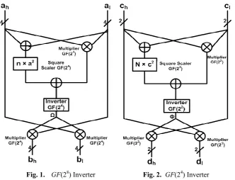
Inversion in GF(28), GF(24) and GF(22). Let the pair (a
h, al) Є GF(24) represents a
ЄGF(28) in terms of Normal basis (X16, X). If b Є GF(28) is inverse of a, then product of a and b is 1.
(5)
Substituting X + X16 = 1, (X16)2 = X16 + n and (X)2 = X + n and solving for b
h and bl.
(6)
Where is multiplication and is addition in GF(24). If = [(ah al) ((ah al)2
n)]-1, then inversion in GF(28) is expressed by following relation.
(7)
The logical structure of GF(28) inverter is shown in figure 1. Similarly, if c Є GF(24)
and it has an inverse d Є GF(24) using normal basis (Y4, Y), then c = c
hY4 + clY, ch, cl ∈GF(22) and d = d
hY4 + dlYdh, dl∈GF(22). If is multiplication and is bitwise
addition in GF(22) and = [(c
h cl) ((ch cl)2 N)]-1, then equation for GF(24)
inversion is given as below:
(8)
The GF(24) inverter is depicted in figure 2. The inversion in GF(22) is same as
squaring and implemented without gates by swapping of bits. If e Є GF(22) is
represented in normal basis (Z2, Z) as e = e
hZ2 + elZ, eh, el ∈ GF(2) and f is the
inverse of e in GF(22) then inversion in GF(22) is:
(9)
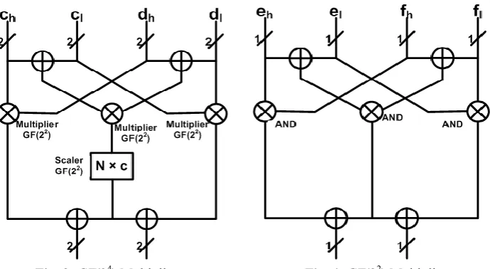
Multiplication in GF(24) and GF(22). The structures of multipliers in GF(24)
and GF(22) in normal basis are derived as below.
(10)
Fig. 1. GF(28) Inverter Fig. 2. GF(24) Inverter
(11)
Where is bit wise addition, is multiplication in GF(22) and Є = (c
h cl) ( dh
dl) N. Similarly GF(22) multiplier in normal basis is represented as:
(12)
represents the bit addition, is AND operation and = (eh el) (fh fl). The
above mentioned structures are illustrated in figure 3 and figure 4 respectively.
Scaling and Squaring in GF(24) and GF(22). In GF(28) and GF(24) inverters
there are constant multiplication operations (n × a2) and (N × c2) and in GF(24)
multiplier there is constant multiplication term (N × c). The combination of squaring and scaling operation results in further optimization [2]. The computation of these terms depends on the values of n in GF(24) and N in GF(22) for the chosen normal
basis. N Є GF (22) and N is not equal to zero or one, therefore N and N+1 are the roots of z2 + z + 1. So depending on the choice of basis, scalars for N and N2 implies
to scalars for z or z2. The two bit factor (N × c) is given in two ways.
(13)
Similarly the square scaling two bit factor (N × c2) is represented in following two
Fig. 3.GF(24) Multiplier Fig. 4.GF(22) Multiplier
(14)
The scaling operation (n x a2) is a four bit factor in GF(28) inverter and its computation in GF(22) depends on the normal basis types and the relation between
norm n and N as in [2]. For computations in GF(24), tables in appendix ‘B’ are used.
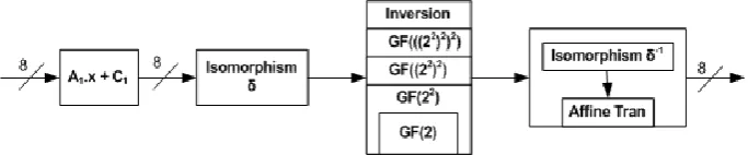
3.2 Generating Isomorphic and Inverse Mapping Functions
The standard SMS4 form is defined by 8 bit vector as coefficients of powers of x which is root of irreducible primitive polynomial in (3). Multiplicative inversion in composite field is computed after a byte in GF(28) is mapped to its composite field representation using isomorphism function δ [6]. After the multiplicative inverse is computed in the composite field, the 8 bit result is mapped back to standard equivalent representation in GF(28) using inverse isomorphic function δ-1. The isomorphic and it inverse mapping is one to one and onto mapping and is represented as 8×8 matrix [10]. If byte s is in standard polynomial basis then it can be represented as a quadratic extension as s = ahX16 + alX, ah, al ∈ GF(24), where each 4 bit
coefficient is represented as c = chY4 +clY, ch, cl ∈ GF(22), each of which is then
further represented as pair of bits e = ehZ2 + elZ in GF(22)/GF(2). If the new byte is
given as t7t6t5t4t3t2t1t0 then we have the following expression [2].
=
.
The values of X, Y and Z are substituted from the conjugate basis chosen and these 8 hexadecimal values with coefficient ti represents the columns of 8 × 8 reverse base
transformation matrix δ-1. The inverse matrix δ is used for changing standard basis to
corresponding composite field representation [2]. The inverse mapping matrix δ-1 is
combined with affine transformation matrix A2 for further optimization as in [6]. The
block diagram of SMS4 S-box is given in the figure below.
Fig. 5. SMS4 S-box Block Diagram
4
Results
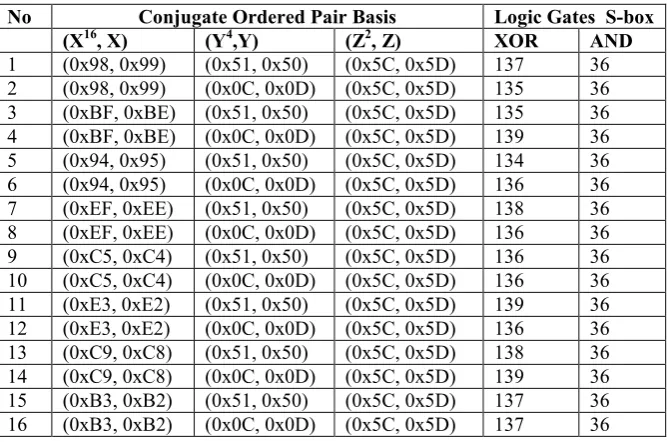
For the possible choices of norms in GF(24) and GF(22) along with the normal basis
at each subfield level satisfying τ = T = 1, we have 16 possible cases as shown in appendix ‘A’. SMS4 S-box design based on each case is fully tested and simulated. The most compact case is the one which gives the least number of XOR gates for implementation. It can be observed from the results in table 1 that choosing different normal basis combination results in small difference in number of XOR gates. These small differences exist due to different mapping matrices and slight differences in the inverter architectures. The matrices operations for mapping, inverse mapping and affine transformation are fully optimized using greedy algorithm [10]. The greedy algorithm operates iteratively on the mentioned matrices determining the occurrences of all possible repeating pairs in the output. The repeating pairs are pre-computed to reduce the number of XOR gates. Our best case S-box design (case 5, table 1) saves 35 XOR gates by application of greedy algorithm.
The GF (28) inverter in normal basis comprises of one GF (24) inverter, three GF(24)
multipliers, one square scaling and two additions in GF(24) as shown in figure 1. One
GF(24) inversion is computed using three multipliers, one inversion, one square
scaling and two additions in GF(22) as depicted in figure 2, where one GF (24)
multiplier comprises of three multipliers, four additions and a scaling operation in
GF(22) as in figure 3. Thus total number of logic gates computed in hierarchical
structure of inverter for our best case S-box is 91 XOR and 36 AND. The structures of multipliers in figure 3 and figure 4 depicts that it requires summation of high and low halves of each input factor. If the same factor is shared by two different multipliers then share factor can save one subfield addition [2]. Thus, a four bit common factor in one GF(24) multiplier can save five XOR gates and a two bit common factor in
GF(22) multiplier can save one XOR gate. In GF(28) inverter in figure 1, all three
GF(24) multipliers have share factors i.e. , ah, a
l are all shared between respective
two GF(24) multipliers thus saving 15 XOR gates. Similarly in GF(24) normal
saving 3 XOR gates. In total 15+3 = 18 XOR gates can be saved by the share factors in GF(28) and GF(24) normal inverters in hardware implementation. Thus total number of gates required for case 5 SMS4 S-box are 73 XOR and 36 AND gates.
Table. 1. All Cases of SMS4 S-box design using Normal basis in GF(((2)2)2)2
No Conjugate Ordered Pair Basis Logic Gates S-box (X16, X) (Y4,Y) (Z2, Z) XOR AND
1 (0x98, 0x99) (0x51, 0x50) (0x5C, 0x5D) 137 36
2 (0x98, 0x99) (0x0C, 0x0D) (0x5C, 0x5D) 135 36
3 (0xBF, 0xBE) (0x51, 0x50) (0x5C, 0x5D) 135 36
4 (0xBF, 0xBE) (0x0C, 0x0D) (0x5C, 0x5D) 139 36
5 (0x94, 0x95) (0x51, 0x50) (0x5C, 0x5D) 134 36
6 (0x94, 0x95) (0x0C, 0x0D) (0x5C, 0x5D) 136 36
7 (0xEF, 0xEE) (0x51, 0x50) (0x5C, 0x5D) 138 36
8 (0xEF, 0xEE) (0x0C, 0x0D) (0x5C, 0x5D) 136 36
9 (0xC5, 0xC4) (0x51, 0x50) (0x5C, 0x5D) 136 36
10 (0xC5, 0xC4) (0x0C, 0x0D) (0x5C, 0x5D) 136 36
11 (0xE3, 0xE2) (0x51, 0x50) (0x5C, 0x5D) 139 36
12 (0xE3, 0xE2) (0x0C, 0x0D) (0x5C, 0x5D) 136 36
13 (0xC9, 0xC8) (0x51, 0x50) (0x5C, 0x5D) 138 36
14 (0xC9, 0xC8) (0x0C, 0x0D) (0x5C, 0x5D) 139 36
15 (0xB3, 0xB2) (0x51, 0x50) (0x5C, 0x5D) 137 36
16 (0xB3, 0xB2) (0x0C, 0x0D) (0x5C, 0x5D) 137 36
5
Comparative Analysis
Our most compact SMS4 S-box comprises of 134 XOR and 36 AND gates with conjugate pair basis (0x94, 0x95), (0x51, 0x50) and (0x5C, 0x5D) respectively. We provide comparison of our most compact case 5 S-box design with the one based on
GF(28) inversion algorithm proposed in [4] that uses polynomial basis. The operations
in the subfield and the number of XOR and AND logic gates required to design SMS4 S-box based on [4] is given in table 3. The matrices computations are optimized using greedy algorithm as in [1].
Table. 2. Logic gates forour Best case SMS4 S-box
Mathematical Operation XOR AND
Affine Trans 1 (A1. x + C1) 29 -
Map GF(28) → GF((22)2)2 15 -
Map inv + Affine Trans 2 17 -
GF(28) Inversion 73 36
Table. 3. Logic Gates forSMS4 S-box based on Polynomial Basis Inverter of [4]
6
Conclusion and Future Work
In this paper we have proposed an improved design for SMS4 S-box based on the combinational logic with a low gate count. The proposed algorithm for computing SMS4 S-box function is based on composite field GF(((22)2)2) and we have simulated all the possible cases of subfield combination depending upon the choice of normal basis, from which we have determined the best case. All the transformation matrices are optimized using greedy algorithm. We have proved that our best case S-box design results in much lower gate count and reduces the complexity by 15% XOR gates and 42% AND gates over the S-box based on the inversion algorithm of [4]. Our compact architecture of SMS4 S-box can save a significant amount of chip area in the hardware implementation of SMS4 in ASICs and it can be used for area constrained and demanding throughput SMS4 integrated circuits for applications ranging from smart cards to high speed processing units. The future work will concentrate on the ASIC implementation of the S-box, where our design can be further improved using the logic gate optimizations depending on specific CMOS standard library.
References
[1] Wolkerstorfer, J., Oswald, E., Lamberger, M.: An ASIC Implementation of the AES Sboxes. In: CT-RSA, LNCS, vol. 2271, pp. 67–78. Springer, Heidelberg (2002)
Mathematical Operation Instances XOR AND
Affine Trans 1 (x.A1+ C1) 1 29 -
Map GF(28) → GF(24)2 1 12 -
Map inv GF(24)2 →GF(28) 1 10 -
Map GF(24) → GF(22)2 1 3 -
Map inv GF(22)2 → GF(24) 1 2 -
Affine Trans 2 (y.A2 + C2). 1 29 -
GF(24) Multiplier 3 45 48
GF(24) Squaring 1 2 -
GF(24) Scaling 1 1 -
GF(24) Addition 2 8 -
GF(22) Multiplier 3 9 15
GF(22) Squaring 1 1 -
GF(22) Scaling 1 1 -
GF(22) Addition 2 4 -
GF(22) Inverter 1 1 -
[2] Canright, D.: A Very Compact Rijndael S-box.Technical Report NPS-MA-04- 001,Naval Postgraduate School (September 2004)
http://web.nps.navy.mil/∼dcanrig/pub/NPS-MA-05-001.pdf [3] Rijmen, V.:Efficient Implementation of the Rijndael S-box (2000)
www.iaik.tugraz.at/RESEARCH/krypto/AES/old/~rijmen/rijndael/sbox.pdf
[4] Bai, X., Xu, Y., Guo, L.: Securing SMS4 Cipher against Differential Power Analysis and its VLSI implementation. In: ICCS (2008)
[5] Rudra, A., Dubey P., Jutla, C., Kumar, V., Rao, J., Rohatgi, P.: Efficient Rijndael encryption implementation with composite field arithmetic. In: CHES 2001, LNCS, pp. 171–184, Heidelberg (2001)
[6] Satoh, A., Morioka, S., Takano, K., Munetoh, S.: A compact Rijndael hardware architecture with S-box optimization. In: ASIACRYPT 2001, LNCS, vol. 2248, pp. 239– 254. Springer Heidelberg (2001).
[7] Mentens, N., Batina, L., Preneel, B., Verbauwhede, I.: A systematic evaluation of compact hardware implementations for the Rijndael S-box. In: CT-RSA, LNCS, vol. 3376, pp 323-333. Springer, Heidelberg (2005)
[8] Office of State Commercial Cipher Administration of China. SMS4 cipher for WLAN products. http://www.oscca.gov.cn/UpFile/200621016423197990.pdf, 2006
[9] Diffie, W., Ledin, G.: SMS4 encryption algorithm for wireless networks. Cryptology ePrint Archive, Report 2008/329, 2008. http://eprint.iacr.org/
[10] Paar, C.:Efficient VLSI architectures for bit parallel computation in Galois fields. Ph.D thesis, Institute for Experimental Mathematics, University of Essen, (1994)
[11] Lidl, R., Niederreiter, H.: Introduction to Finite Fields and their Applications. Cambridge University Press, New York, USA (1986)
[12] Deschamps, J., Sutter, G., Imana, J.: Hardware Implementation of Finite Field Arithmetic. McGraw-Hill Professional ISBN: 978-0-07-154582-2 (2009)
[13] Erickson, J., Ding, J., Christensen, C.: Algebraic cryptanalysis of SMS4: Grobner basis attack and SAT attack compared. In : ICISC (2009)
Appendix A:
GF
(2
8) Representation for SMS4 S-Box
A.1 The table below gives the decimal, hexadecimal and binary values of the
GF(28) generated modulo irreducible primitive polynomial f(x) =
x8+x7+x6+x5+x4+x2+1. Let A be the root of f(x) then the field generated with
respective names of elements is as below:
Dec Hex Binary θi Name Dec Hex Binary θi Name 78 4E 01001110 θ188 j64 123 7B 01111011 θ238 β 79 4F 01001111 θ61 k64 124 7C 01111100 θ11 F 80 50 01010000 θ17 α 125 7D 01111101 θ253 q2 81 51 01010001 θ68 α4 126 7E 01111110 θ32 A32 82 52 01010010 θ105 a8 127 7F 01111111 θ208 G16 83 53 01010011 θ129 B128 128 80 10000000 θ7 D 84 54 01010100 θ154 b32 129 81 10000001 θ87 g8 85 55 01010101 θ39 d8 130 82 10000010 θ166 b8 86 56 01010110 θ120 H8 131 83 10000011 θ201 d2 87 57 01010111 θ196 J64 132 84 10000100 θ145 M16 88 58 01011000 θ177 N16 133 85 10000101 θ172 Q4 89 59 01011001 θ230 e 134 86 10000110 θ74 P2 90 5A 01011010 θ224 D32 135 87 10000111 θ132 E128 91 5B 01011011 θ234 g 136 88 10001000 θ29 f32 92 5C 01011100 θ170 λ2 137 89 10001001 θ218 c 93 5D 01011101 θ85 λ 138 8A 10001010 θ94 j32 94 5E 01011110 θ115 e128 139 8B 10001011 θ158 k32 95 5F 01011111 θ216 N8 140 8C 10001100 θ112 D16 96 60 01100000 θ139 L128 141 8D 10001101 θ117 g128 97 61 01100001 θ246 l 142 8E 10001110 θ185 e64 98 62 01100010 θ251 q4 143 8F 10001111 θ108 N4 99 63 01100011 θ22 F2 144 90 10010000 θ214 c8 100 64 01100100 θ242 j 145 91 10010001 θ232 f 101 65 01100101 θ244 k 146 92 10010010 θ194 F64 102 66 01100110 θ161 G32 147 93 10010011 θ127 q128 103 67 01100111 θ64 A64 148 94 10010100 θ59 h64
104 68 01101000 θ37 P 149 95 10010101 θ179 h4
105 69 01101001 θ66 E64 150 96 10010110 θ182 c64 106 6A 01101010 θ83 b4 151 97 10010111 θ71 f8 107 6B 01101011 θ228 d 152 98 10011000 θ206 h16
108 6C 01101100 θ91 c32 153 99 10011001 θ236 h
A.2 The minimal polynomials over GF(2) and their respective conjugate roots in terms of θi are presented in the following table.
Dec Hex Binary θi Name Dec Hex Binary θi Name
168 A8 10101000 θ155 e4 212 D4 11010100 θ84 K4
169 A9 10101001 θ198 N64 213 D5 11010101 θ215 n8
170 AA 10101010 θ40 C8 214 D6 11010110 θ229 j2
171 AB 10101011 θ124 m128 215 D7 11010111 θ233 k2
172 AC 10101100 θ121 j128 216 D8 11011000 θ92 L4
173 AD 10101101 θ122 k128 217 D9 11011001 θ183 l8
174 AE 10101110 θ197 L64 218 DA 11011010 θ164 P32
175 AF 10101111 θ123 l128 219 DB 11011011 θ72 E8
176 B0 10110000 θ178 Q16 220 DC 11011100 θ98 J32 177 B1 10110001 θ70 M64 221 DD 11011101 θ60 H4 178 B2 10110010 θ231 p8 222 DE 11011110 θ192 B64 179 B3 10110011 θ126 p128 223 DF 11011111 θ180 a4 180 B4 10110100 θ225 H32 224 E0 11100000 θ81 K16 181 B5 10110101 θ19 J 225 E1 11100001 θ95 n32 182 B6 10110110 θ235 n4 226 E2 11100010 θ249 p2
183 B7 10110111 θ42 K2 227 E3 11100011 θ159 p32
184 B8 10111000 θ171 g4 228 E4 11100100 θ49 J16 185 B9 10111001 θ131 D128 229 E5 11100101 θ30 H2 186 BA 10111010 θ86 Q2 230 E6 11100110 θ46 L2 187 BB 10111011 θ200 M8 231 E7 11100111 θ219 l4 188 BC 10111100 θ116 f128 232 E8 11101000 θ56 D8 189 BD 10111101 θ107 c4 233 E9 11101001 θ186 g64 190 BE 10111110 θ217 h2 234 EA 11101010 θ142 f16 191 BF 10111111 θ157 h32 235 EB 11101011 θ109 c128 192 C0 11000000 θ140 M128 236 EC 11101100 θ222 l32 193 C1 11000001 θ101 Q32 237 ED 11101101 θ113 L16 194 C2 11000010 θ247 q8 238 EE 11101110 θ103 h8
195 C3 11000011 θ44 F4 239 EF 11101111 θ118 h128
Name Minimal Polynomial Conjugate Roots (θi)
1 x + 1 θ0
λ x2 + x + 1 θ85 , θ170
α x4 + x + 1 θ17 , θ34, θ68 , θ136 β x4 + x3 + 1 θ238 , θ221 , θ187 , θ119 γ x4 + x3 + x2 + x + 1 θ51 , θ102 , θ204 , θ153
Appendix B:
Tables for
GF
(2
4) Computations
B.1 The table below gives the decimal, hexadecimal and binary values of the
GF(24) generated modulo irreducible primitive polynomial g(x) = x4 + x + 1. Let α be
the root of g(x) then the field generated with respective names of elements is as below:
Dec Hex ANF i Bin i i Name
0 00 0 0000 - 0
1 01 x 0001 0 1
2 02 x2 0010 1 α
3 03 x + 1 0011 4 α4
4 04 x2 0100 2 α2
5 05 x2 + 1 0101 8 α8
6 06 x2 + x 0110 5 λ
7 07 x2 + x + 1 0111 10 λ2
8 08 x3 1000 3 γ
9 09 x3 + 1 1001 14 β
10 0A x3 + x 1010 9 γ8
11 0B x3 + x + 1 1011 7 β8
12 0C x3 + x2 1100 6 γ2
13 0D x3 + x2 + 1 1101 13 β2
14 0E x3 + x2 + x 1110 11 β4
15 0F x3 + x2 + x + 1 1111 12 γ4
B.2 The table below gives the minimal polynomials over GF(2) and their respective conjugate roots in terms of i are presented using irreducible primitive
polynomial g(x) = x4 + x + 1.
Name Polynomial Minimal Conjugate Roots (θi)
1 x + 1 0
λ x2 + x + 1 5 , 10
α x4 + x + 1 , 2, 4 , 8
β x4 + x3 + 1 14, 13 , 11, 7
B.3 The addition table in GF(16) using the naming convention in table A.1 is given below:
0 1 α α2 γ α4 λ γ2 β8 α8 γ8 λ2 β4 γ4 β2 β 0 0 1 α α2 γ α4 λ γ2 β8 α8 γ8 λ2 β4 γ4 β2 β
1 1 0 α4 α8 β α λ2 β2 γ8 α2 β8 λ γ4 β4 γ2 γ
α α α4 0 λ γ8 1 α2 β4 β λ2 γ α8 γ2 β2 γ4 β8
α2 α2 α8 λ 0 γ2 λ2 α γ γ4 1 β4 α4 γ8 β8 β β2
γ γ β γ8 γ2 0 β8 β4 α2 α4 β2 α γ4 λ λ2 α8 1
α4 α4 α 1 λ2 β8 0 α8 γ4 γ λ β α2 β2 γ2 β4 γ8
λ λ λ2 α2 α β4 α8 0 γ8 β2 α4 γ2 1 γ β β8 γ4
γ2 γ2 β2 β4 γ α2 γ4 γ8 0 λ2 β λ β8 α α4 1 α8
β8 β8 γ8 β γ4 α4 γ β2 λ2 0 β4 1 γ2 α8 α2 λ α
α8 α8 α2 λ2 1 β2 λ α4 β β4 0 γ4 α β8 γ8 γ γ2
γ8 γ8 β8 γ β4 α β γ2 λ 1 γ4 0 β2 α2 α8 λ2 α4
λ2 λ2 λ α8 α4 γ4 α2 1 β8 γ2 α β2 0 β γ γ8 β4
β4 β4 γ4 γ2 γ8 λ β2 γ α α8 β8 α2 β 0 1 α4 λ2
γ4 γ4 β4 β2 β8 λ2 γ2 β α4 α2 γ8 α8 γ 1 0 α λ
β2 β2 γ2 γ4 β α8 β4 β8 1 λ γ λ2 γ8 α4 α 0 α2
β β γ β8 β2 1 γ8 γ4 α8 α γ2 α4 β4 λ2 λ α2 0
B.4 The multiplication table in GF(16) is given as below:
0 1 α α2 γ α4 λ γ2 β8 α8 γ8 λ2 β4 γ4 β2 β
0 0 0 0 0 0 0 0 0 0 0 0 0 0 0 0 0
1 0 1 α α2 γ α4 λ γ2 β8 α8 γ8 λ2 β4 γ4 β2 β
α 0 α α2 γ α4 λ γ2 β8 α8 γ8 λ2 β4 γ4 β2 β 1
α2 0 α2 γ α4 λ γ2 β8 α8 γ8 λ2 β4 γ4 β2 β 1 α
γ 0 γ α4 λ γ2 β8 α8 γ8 λ2 β4 γ4 β2 β 1 α α2
α4 0 α4 λ γ2 β8 α8 γ8 λ2 β4 γ4 β2 β 1 α α2 γ
λ 0 λ γ2 β8 α8 γ8 λ2 β4 γ4 β2 β 1 α α2 γ α4
γ2 0 γ2 β8 α8 γ8 λ2 β4 γ4 β2 β 1 α α2 γ α4 λ
β8 0 β8 α8 γ8 λ2 β4 γ4 β2 β 1 α α2 γ α4 λ γ2
α8 0 α8 γ8 λ2 β4 γ4 β2 β 1 α α2 γ α4 λ γ2 β8
γ8 0 γ8 λ2 β4 γ4 β2 β 1 α α2 γ α4 λ γ2 β8 α8
λ2 0 λ2 β4 γ4 β2 β 1 α α2 γ α4 λ γ2 β8 α8 γ8
β4 0 β4 γ4 β2 β 1 α α2 γ α4 λ γ2 β8 α8 γ8 λ2
γ4 0 γ4 β2 β 1 α α2 γ α4 λ γ2 β8 α8 γ8 λ2 β4
β2 0 β2 β 1 α α2 γ α4 λ γ2 β8 α8 γ8 λ2 β4 γ4
![Table. 3. Logic Gates for SMS4 S-box based on Polynomial Basis Inverter of [4]](https://thumb-us.123doks.com/thumbv2/123dok_us/1876834.1244413/9.595.177.418.167.378/table-logic-gates-sms-based-polynomial-basis-inverter.webp)
