Thesis by
Christopher P. Michael
In Partial Fulfillment of the Requirements for the Degree of
Doctor of Philosophy
California Institute of Technology Pasadena, California
2009
c 2009
Acknowledgments
For the reasons that you may know and those you may not . . .
Thank you, Oskar.
Thank you, Tom. Thank you, Raviv and Matt. Thank you, Matt, Kartik, and Paul. Thank you, Scott, Vijit, Homan, Andrew, Richard, and Robin. Thank you, Jessie, Qiang, Thiago, and Ryan. Thank you, Auna, Mike, Dave, and Sameer. Thank you, Ernie. Thank you, Eleonora, Lyn, and Janet.
Thank you, Chris and Masaya. Thank you, Naomi and Dave. Thank you, Jean, Tim, Mike, Bill, and Jerry. Thank you, Bill and Maxim.
My gratitude goes to the Gordon and Betty Moore Foundation, the National Science Foun-dation, and the Bill and Melinda Gates Foundation.
Thank you, Mom, Dad, and Jessie.
Abstract
Since Jack Kilby recorded his “Monolithic Idea” for integrated circuits in 1958, microelec-tronics companies have invested billions of dollars in developing the silicon material system to increase performance and reduce cost. For decades, the industry has made Moore’s Law, concerning cost and transistor density, a self-fulfilling prophecy by integrating technical and material requirements vertically down their supply chains and horizontally across com-petitors in the market. At recent technology nodes, the unacceptable scaling behavior of copper interconnects has become a major design constraint by increasing latency and power consumption—more than 50% of the power consumed by high speed processors is dissipated by intrachip communications. Optical networks at the chip scale are a potential low-power high-bandwidth replacement for conventional global interconnects, but the lack of efficient on-chip optical sources has remained an outstanding problem despite significant advances in silicon optoelectronics. Many material systems are being researched, but there is no ideal candidate even though the established infrastructure strongly favors a CMOS-compatible solution.
Contents
Acknowledgments iv
Abstract v
Glossary of Acronyms xii
Preface xiv
1 Microdisk Optical Cavities 1
1.1 Quasi-normal Modes . . . 3
1.2 Coupled-Mode Theory . . . 8
1.2.1 Coherent Backscattering . . . 10
1.2.2 Microdisk-Waveguide Coupling . . . 12
1.3 Cavity Parameters . . . 17
2 “Dimpled” Fiber-Taper Probe 21 2.1 Taper Pulling and Molding . . . 22
2.2 Microphotonic Testing with a Dimple-Taper Waveguide . . . 25
2.2.1 Noise Measurements . . . 27
2.2.2 Dense Si Microdisk Array . . . 29
2.2.3 Planar Si-SiO2 Microring via RIE Processing . . . 31
2.2.4 Planar Si-SiO2 Microring via LOCOS Processing . . . 32
2.3 Conclusions . . . 35
3 Linear Absorption in AlGaAs and GaAs Microcavities 36 3.1 AlxGa1−xAs Samples and Processing . . . 37
4 Optical Processes in Epitaxial c-Er2O3 on Silicon 43
4.1 Rare-Earth Ions in the R2O3 Bixbyite Lattice . . . 44
4.1.1 Growth . . . 47
4.1.2 Processing . . . 50
4.2 Optical Properties . . . 52
4.2.1 Absorption and Emission Spectra for the 4I 13/2→4I15/2 Transition . 53 4.2.2 Upconversion . . . 57
4.2.3 Effective 4I 13/2 Lifetime . . . 60
4.2.4 Power-Dependent Radiative Efficiency . . . 63
4.2.5 Cavity Polaritons . . . 67
4.2.5.1 Low-Temperature Polaritons . . . 69
4.2.5.2 High-Temperature Polaritons . . . 76
4.2.6 Rate Equation Estimates . . . 82
4.3 Conclusions . . . 84
A Experimental Supplement 86 A.1 Mach-Zehnder Interferometer . . . 86
A.2 Pulse Optimization for EOSPACE Modulators . . . 90
A.3 Effective Index for the HE11 Mode . . . 92
A.4 Coherent Coupling to a Uniform Density of Dipoles . . . 92
B Calculation of the β-Factor for Er2O3 Microdisks 95
List of Figures
1.1 Microdisk geometry . . . 4
1.2 FEM simulation of field components for TE and TM microdisk modes . . . . 7
1.3 Comparison of effective-index and FEM models for microdisk QNMs . . . 9
1.4 Illustration of microdisk-waveguide coupling . . . 13
1.5 Power conservation and phase for coupling to a doublet resonance . . . 14
1.6 Comparison of cavity loading for singlet and doublet modes . . . 17
2.1 Process for producing dimpled fiber-taper couplers . . . 23
2.2 The “dimpled” fiber-taper waveguide probe . . . 25
2.3 Dimple taper profile as a function of fiber tension . . . 26
2.4 Basic arrangement for microcavity transmission measurements . . . 26
2.5 Reducing mechanical noise through higher taper tension. . . 28
2.6 Testing demonstration: dense microdisk array . . . 30
2.7 Testing demonstration: planar microring . . . 31
2.8 Testing demonstration: LOCOS process development . . . 33
3.1 AlxGa1−xAs microdisk resonators . . . 38
3.2 Summary of measured resonance parameters for AlxGa1−xAs microdisks . . . 38
3.3 Sample surface roughness measurement on a AlGaAs microdisk . . . 40
4.1 Rare-earth ions in the R2O3 lattice . . . 45
4.2 Er2O3 grown via ALE on Si(111) . . . 48
4.3 Processing Er2O3 microdisk cavities . . . 51
4.4 Er2O3 microdisk transmission spectrum (R≈20µm) . . . 53
4.5 Emission and absorption spectra for the 4I13/2→4I15/2 transition . . . 54
4.7 Upconversion behavior . . . 59
4.8 Measurement of the 4I 13/2 lifetime. . . 61
4.9 Power-dependent radiative efficiency of the 4I13/2→4I15/2 transition . . . 65
4.10 Cavity-polariton spectra at T = 8.6 K . . . 70
4.11 Dispersion and absorption for Z1→Yx transitions atT = 8.6 K . . . 75
4.12 Spoked microdisks used for high-temperature polariton measurements . . . . 77
4.13 Schematic layout for polariton pump-probe measurements. . . 78
4.14 Observation of Rabi splitting at high temperature . . . 80
A.1 Calibration of wide spectra using a fiber-based Mach-Zehnder interferometer 89 A.2 Comparison of neff values for the HE11 mode . . . 93
List of Tables
2.1 Average cavity mode parameters for microdisk array . . . 30
3.1 Summary of GaAs and AlxGa1−xAs material absorption rates. . . 41
4.1 Lattice constant and mismatch for R2O3 bixbyite crystals on (111)Si . . . 49
4.2 Summary of observed cavity-polaritons at T = 8.6 K . . . 71
Glossary of Acronyms
AFM Atomic force microscopy ALE Atomic layer epitaxy APD Avalanche photodiode BOX Buried oxide
CCD Charge-coupled device
CMOS Complementary metal-oxide-semiconductor cQED Cavity quantum electrodynamics
CW Continuous wave
DBR Distributed Bragg reflector DCA Digital communications analyzer EDFA Erbium-doped fiber amplifier
EOM Electro-optic modulator FEM Finite-element method
FPC Fiber polarization controller FSR Free spectral range
GVD Group velocity dispersion LOCOS Local oxidation of silicon
LPF Long-pass filter
OSA Optical spectrum analyzer PD Photodiode
PECVD Plasma-enhanced chemical vapor deposition PL Photoluminescence
PLC Photonic lightwave circuit PM Polarization maintaining PML Perfectly matched layer
QD Quantum dot QNM Quasi-normal mode
RHEED Reflection high-energy electron diffraction RIE Reactive ion etch
RS Russell-Saunders
SEM Scanning electron microscopy SOI Silicon-on-insulator
SPF Short-pass filter
TEM Transmission electron microscopy VOA Variable optical attenuator WGM Whispering gallery mode
XRD X-ray diffraction
Preface
When I first joined Oskar Painter’s group in early 2005, his first students were beginning to accelerate into their thesis projects and reap the benefits from their hard work setting up the labs. Matt Borselli and Tom Johnson’s attempts at Raman lasing in silicon were being thwarted by dynamic free-carrier effects, and they were addressing surface-state absorption and passivation issues during their drive toward microlasers with a silicon core and erbium-doped cladding. Except for a few late processing runs, Paul Barclay had largely disappeared from Steele (along with his 852-nm laser) to work in the Mabuchi lab, and Kartik Srinivasan was studying microdisk lasers containing quantum dots while biding his time to build up the cQED experiment.
During that summer, I joined Kartik on the quantum dot project, and I began to learn how to pull fiber-tapers and how to test microresonators with them. Luckily, Colin Chrystal was Matt’s SURF student that summer, and the taper-pulling program he developed has been invaluable to me ever since. With my vision, I rely entirely upon the interference in the fiber transmission because I have trouble seeing the taper. If it were not for one afternoon when I ripped the acrylic box off the puller and installed a camera, I still might not believe Oskar and Paul about the fiber “bowing.” Throughout that first year, I pulled a lot of tapers, and I tried to adapt Paul’s epoxy microjoint technique to make pigtailed taper-coupled resonators for the cryostat. However despite exotic cryo- and space-ready epoxies, we were never able keep the taper attached below∼200 K. The various manufacturers were fairly defensive of their products and utterly flabbergasted when we told them we were using less than one picoliter per joint. After we realized we would have to buy low-temperature piezoelectric stages, I moved to developing the dimple tapers, which have become quite successful and reduce the processing time for our typical devices by ∼40%.
working towards the strong coupling regime in cQED using quantum dots. The original objective was to compare Kartik’s RIE (Ar:Cl2) with Kevin’s wet chemical etches (HBr) of AlxGa1−xAs and to understand why both methods seemed to underperform at shorter wavelengths. Unfortunately, the only method to assess the procedures (and not just lone exceptional devices) was to study many modes on many resonators at many wavelengths and identify statistical trends in the resulting heap of data. Since Kartik and Oskar were pretty sure this was a material issue, we reduced the scope to study only the HBr process (Kevin also gained a processing assistant so he would not actually have to make these devices). I got a lot of practice taper testing and quickly learned about microdisks, especially once we realized the edge roughness was different on our two material samples. Through the early summer, I worked to pile up data between classes and being hammered by the APh 24 lab, located in the lifeless cave that would shortly become the Kavli Nanoscience Institute. During that time I also decided to switch off the quantum dot project. Kartik was running past microlasers and master equations while I was still dealing with resonator coupling and holography labs. Ironically, Matt was simultaneously developing some more advanced single-shot techniques to separate scattering and absorption that would have saved me a lot of time and effort—I found out about these while reading his thesis a few months after I had finished taking my data.
So I packed my bags and landed in silicon photonics. After doing some basic silicon testing for the dimple paper, our intention was that I would continue work with the Er3+ -doped silica from InPlane Photonics that Matt had left after his graduation. However, that fall we were presented with the opportunity to switch our DARPA program to work with Translucent in developing Er2O3. Oskar and I made the switch realizing the big-risk/big-reward potential. At the very least, it would temporarily free me from low-loss surface-senstive processing and give us exclusive access to new material (unlike the crowded field of erbium-doped glasses). I had already broken my rule #1 for choosing thesis topics (no cryogenics) so breaking rule #2 (no exotic materials) did not seem that bad—especially since the growers (Vijit Sabnis and Homan Yuen) were ready and willing to ship me more material than I could ever deal with. I am still waiting to break rule #3 (no ultrahigh vacuum) and give MBE a shot.
films at a battery of chemicals, of which most did nothing. I proceeded optimistically as Homan and Vijit addressed material problems at about the same pace I was figuring out the processing and testing aspects. The first disks I made with H2SO4 produced weak, but measurable, PL and exhibited the transmission features that would later be identified as cavity-polaritons at room temperature. By March of 2007, we were beginning to become concerned with the upconversion and our inability to see any absorption saturation. In June, I figured out the Ar+ milling, made a bunch of samples, and then did not go back into the clean room for over a year (except to train people and pester Raviv Perahia). Once free from the clean room, I began gaining dominion over equipment in the test lab, which has provided me far too much contact with the New Focus laser repair department.
That fall, after a year on the project, we were beginning to get frustrated, but I keep myself busy with absorption spectra, radiative efficiency, upconversion, and polaritons at high and low temperatures. Vijit and Homan had moved on to work on starting a new company, but Translucent was bringing on new people. At this point, I also began some adventures into cQED by helping Kartik with some of his quantum dot measurement and testing my own disks in the cryostat. I worked throughout 2008 investigating the lifetime and polariton behaviors. Some of the data could have been obtained more quickly with unprocessed films and free-space optics. However, my unorthodox measurements fit within our microcavity infrastructure, and we were always optimistic that we would uncover some physics that would allow us to quickly proceed. Although with the rare-earth studies from the 1970s and a few rate equation parameters in hand, a coherent picture was emerging that Er2O3 is not a suitable laser material, and the weak coherent coupling to each ion made the ubiquitous Rabi splitting depressingly classical. I began a few last-ditch efforts to achieve lasing that pushed our equipment to the limits and the material beyond its damage threshold because we had invested a lot of time and energy. A Λ-system laser between carefully chosen Stark levels at 8 K is a viable option, but the benefits probably do not outweigh the effort. I decided to leave many questions unanswered concerning upconversion lasing at green wavelengths in the current material after burning standing-wave gratings into three disks and outright vaporizing a fourth. There is a subtle lesson here about knowing when to terminate an experiment.
photons to other wavelengths using Y2O3 or Gd2O3alloys. I was exposed to a wide range of photonics and atomic physics trawling for immediate applications and results to utilize the current material, which really is an initial step in a much more ambitious material science and engineering program. Even though much of this thesis is focused on absorption rather than emission, I take solace in the difficult road to Maiman’s first ruby laser and that a com-mercially acceptable solution still does not exist to generate gain for optical interconnects on CMOS microelectronics.
After presenting the formalism for coupling to WGM cavities used throughout these measurements, this thesis is divided according to material systems. Silicon microresonators are presented in chapter 2 with details of the dimpled taper probes, which initially saw their greatest use in prototyping Si devices and fabrication methods. A sample analysis of loss in AlxGa1−x is presented in chapter 3, and chapter 4 concentrates on Er2O3. Ancillary experimental and theoretical details are reserved for the appendices.
Chapter 1
Microdisk Optical Cavities
The resonant circulation of electromagnetic waves enables a variety of macroscopic systems from lasers to interferometric gravitational wave detectors, but recent pressure from the telecommunications and microelectronics industries, along with more fundamental research programs, has driven the development of wavelength-scale optical cavities, waveguides, and other components. Microphotonic cavities can be designed to give a large electric field strength per photon, a sparse spectrum of optical modes, and great sensitivity to the struc-ture’s surfaces [1, 2]. By combining these attributes with a high circulating intensity (i.e., low field decay rate for the optical mode), microcavity physics is central to many sub-jects including low-threshold and “thresholdless” lasers [3], control of spontaneous emission through the Purcell Effect [4, 5], nonperturbative light-matter interactions [2, 6], low-power nonlinear optics [7, 8], chemical and biological “lab-on-a-chip” devices [9], and cavity op-tomechanics [10].
without a dielectric discontinuity at the center of the cavity [18], and whispering-gallery microresonators (e.g., spheres [19], disks [20], and toroids [21]) provide a rich spectrum of modes with low intrinsic loss.
While significant work is focused on cavity design, material properties are of equal concern in many applications. These properties include both bulk quantities (absorption coefficient, radiative and nonradiative relaxation rates, etc.) and surface quantities (absorp-tion by surface states, surface recombina(absorp-tion velocity, etc.). Microcavities are a convenient tool for assessing material quality because they offer a long effective interaction length and measurable losses associated with input/output coupling. Device attributes associated with material processing (surface roughness, passivation layers, etc.) can also be investigated once bulk effects are adequately understood.
To maximize their utility for material studies, microcavities should be trivial to design with low intrinsic loss, easy to fabricate in a variety of materials, and straightforward to identify fabricated imperfections without optical measurements. Compared to other geometries, microdisk resonators offer an attractive combination of simplicity and material flexibility. Disks with diameters (thicknesses) ≫λo/nd (>λo/2nd) support a large number of modes with very low radiation loss and require only a single material layer,1 whereλo is the free-space wavelength andndis the refractive index of the disk material. The quality of the fabrication process for these devices can be easily evaluated by the surface roughness, unlike photonic crystals that require fault-tolerant designs [22] or precise simulation of the as-fabricated structures [23]. Microdisks are also robust against subtle leaky geometric variations as in micropillars [24, 25] and microrings [26].2 Microspheres and toroids offer many of the same advantages along with the lowest optical loss for any microcavity structure, which makes these devices extremely sensitive to refractive index changes in their modes’ evanescent tail [28–30], but the glass reflow procedure limits their material range to doped silica (e.g., through sol-gel deposition [31, 32] or ion implantation [33, 34]) or postreflow surface coatings [35, 36]. While replica molding techniques extend the toroid’s versatility to cured polymers [37], processing methods for crystalline toroids (e.g., silicon [38]) are not as mature as for microdisks. In this chapter, the quasi-normal whispering gallery modes
1Excluding a sacrificial substrate that must be undercut to form the disk’s pedestal.
2The whispering gallery modes of a microdisk with low refractive index can couple to modes with the
(WGMs) of a microdisk resonator are discussed, and the coupled-mode theory and cavity parameters used throughout this work are presented.
1.1
Quasi-normal Modes
The normal modes of a system are solutions to the appropriate time-independent wave equation with the condition that the wave amplitude vanishes at the system boundary (either at infinity or the boundary of a more suitable domain), as for the optical field in an ideal Fabry-P´erot cavity or the elastic vibrations of a perfectly isolated rigid body. Under this constraint, the field magnitude is conserved, and the eigenvalues are real. The quasi-normal modes (QNM) of an open system are solutions to the same wave equation with an outgoing traveling-wave boundary condition that causes the field to decay [39]. In this classical analysis, the nature of the coupling to the bath of radiation modes is concealed unlike the quantum treatment of dissipation where the bath’s degrees of freedom are included and later removed using specific assumptions [40].
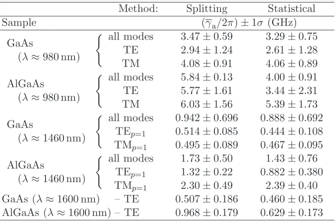
The microdisk structure consists of a planar slab with radius R and height h as in Fig. 1.1(a)—we assume the pedestal and substrate are undercut far enough to have little overlap with the cavity field. While analytic solutions for this geometry do not exist, the cavity modes can be found with reasonable accuracy using a 2D effective-index model. In Refs. [41, 42], the QNMs are further simplified by using exponential decay to describe fields outside the cavity. These real normal-mode eigenvalues do not describe radiation loss, but this analysis can be extended to include radiating fields and complex eigenvalues.3 Further insight into the modes’ behavior can also be gained from a conformal coordinate transformation and the WKB approximation [44, 45], but semianalytic solutions without this transform have been most useful for quickly evaluating dispersion characteristics and providing accurate starting values for targeted numerical eigenvalue solvers.
Starting with the electromagnetic wave equation for a linear piecewise-homogeneous medium in the absence of free charges and currents,
∇2F~ −n
2(~r)
c2
∂2F~
∂t2 = 0, (1.1)
where F~ ∈ {E, ~~ H}, the standard linear constitutive relations are D~ = ǫ(~r)E~ and B~ =
whereξ =n2eff/n2o for TE modes and ξ= 1 for TM modes.
Equation 1.6 can be solved numerically in the complex plane using a 2D minimization routine starting near the real axis [ℜ(ko) ≫ ℑ(ko)]. There will be multiple solutions to Eq. (1.6) for a given angular momentum (m) corresponding to modes of different radial order p [number of antinodes for Hz or Ez along ˆr as in Fig. 1.1(a)]. The index p also qualitatively describes the momentum along the radial direction. Hence, the fundamental (p= 1) radial mode for a givenmwill have the lowest|ko|because higherpmodes will have a larger total momentum if the angular component is fixed. In general for two modes with the same|ko|ifp1< p2, thenm1 > m2. Microdisks also support modes with higher vertical order (more than oneFzantinode along ˆz) which can be found with Eq. (1.6) by using neff for the appropriate order slab mode; however, the devices in this work only support the fundamental slab modes. For completeness, the condition to cut off the second-order mode is
2h λo
q
n2
d−n2o<1, (1.7)
which corresponds toh= 233 nm in Si (nd = 3.476) at λo = 1550 nm; the fundamental TE and TM modes are never cut off in a symmetric slab waveguide. Throughout this thesis, microdisk modes are commonly organized in families according to polarization and radial order (e.g., TEp=2); within these families, consecutive modes (∆m=±1) have a relatively small free spectral range, comparable radiation loss, and similar phase velocity at the disk edge—which is pertinent to WGM-waveguide coupling.
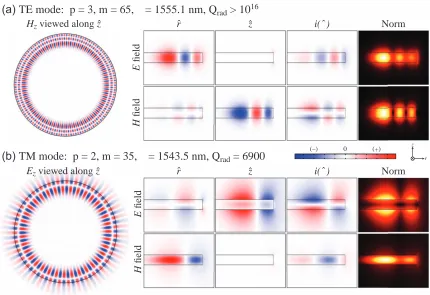
While the effective-index solution provides an efficient method for finding the QNM eigenvalues with modest computational resources, numerical models using the finite ele-ment method (FEM) are more flexible for variable structures and calculations involving the full 3D geometry. Finite-element simulation of axially symmetric resonators can be accomplished using Comsol’s Multiphysics/Femlab platform by incorporating theeimϕ de-pendence into a fully vectorial Cartesian waveguide solver.5 In these models, the 3D cavity and cladding are represented by a cross section in the ˆr-ˆz plane, and a targeted eigenvalue solver finds numerically exact field profiles for the QNMs at a givenm value, as in Fig. 1.2. Full 3D simulations provide no additional information for these studies and are too
mem-5This code was originally developed by S. Spillane [50, 51]. M. Borselli and T. J. Johnson reconfirmed
E
field
H
field
→
→
r z i(φ) Norm
E
field
H
field
→
→
ˆ ˆ ˆ
Hzviewed along zˆ
(a) TE mode: p = 3, m = 65, λ = 1555.1 nm, Qrad > 1016
(b) TM mode: p = 2, m = 35, λ = 1543.5 nm, Qrad = 6900 (–) 0 (+) r z φ
rˆ zˆ i(φ)ˆ Norm
Ezviewed along zˆ
Figure 1.2: Sample FEM simulations of field components for (a) TE and (b) TM modes in a Si microdisk with R = 7.5µm and h = 210 nm showing the region 5 ≤ r ≤ 8µm. Simulations in the ˆr- ˆϕplane utilize the sameneff approximation as Eq. (1.3a), but they are less accurate than the solutions to the ˆr-ˆz FEM models or Eq. (1.6). The notation “i( ˆϕ)” indicates theFϕ components areπ/2 out of phase.
ory intensive for typical desktop computers.6 When setting the geometry, the disk and cladding must be bound by perfectly matched layers (PMLs) that allow energy to escape the simulated domains in order to properly account for radiation losses [53]. These PMLs have complex anisotropic permittivity and permeability that quickly attenuate fields along a single direction without producing spurious reflections. By including PMLs thick enough to fully absorb the radiated waves, both highly confined and highly lossy modes can be found withℑ(ko) varying by more than 1014×as in Fig. 1.2. The quantityℜ(ko)/2ℑ(ko) is approximately 2πtimes the number of optical cycles that occurs while the field decays—this value is later identified as the radiation limited quality factor Qrad.
These quasi-3D FEM models can be used to address two important aspects of real
microdisks that are not captured by the effective-index approximation: 1) the disk edge is not perfectly vertical and 2) surface effects. First, the primary objective during disk fabrication is minimizing surface roughness to reduce scattering losses, and the optimized anisotropic etches do not generally produce vertical sidewalls. Slanted edges couple the TE and TM polarizations by breaking the disk’s vertical symmetry, which can occasionally produce hybrid modes if a TE and a TM mode are nearly degenerate and have the samem. The TE/TM labels are no longer rigorously accurate with slanted walls because significant longitudinal components may exist, but modes are conventionally identified as “TE” if |Er|>|Ez|at the disk’s midplane. For most general considerations, the bevelled edge only marginally increases the radiation losses [54, 55]. Second, Fig. 1.2 illustrates TM modes are significantly more sensitive to the top and bottom surfaces while the TE modes have greater overlap with the sidewall. This difference has practical consequences that will be discussed later, such as absorption by surface states [56].
Comparing approximate effective-index solutions with FEM results in Fig. 1.3 for two disk microdisk devices indicates the effectiveness of Eq. (1.6) to quickly explore wide areas in parameter space. The approximate solutions take .0.5 s to compute without previous information about the QNMs. Alternatively, FEM simulations take ∼1–2 min with a rea-sonable mesh resolution [<0.05λ/n(~r)] and a good initial guess for the desired eigenvalue (∆λo.5 nm); however, they can be accelerated (∼10 s) during parametric studies if better guesses can be supplied (∆λo .0.2 nm). In Fig. 1.3, the effective-index solutions overesti-mate λo found using the FEM by 3.6 nm and underestimateℑ(ko) by 1.9× on average.
1.2
Coupled-Mode Theory
Coupled mode analysis is a general framework to describe the evolution of optical fields due to perturbations that do not significantly alter the system’s eigenmodes [57]. As is common in perturbation theories, a total field in a system (driven with a laser atω=ωℓ) is expanded as
~
E(~r, t) =e−iωℓtX
j
aj(t)E~jo(~r), (1.8)
in terms of slowly varying amplitudesaj(t) and the system’s unperturbed QNM field profiles
~
1440 1460 1480 1500 1520 1540 1560 1580 1600 1620
105
Wavelength (nm) 1420
1010
1015
102
104
106
108
1010 1440 1460 1480 1500 1520 1540 1560 1580 1600 1620
Wavelength (nm)
TE modes: Er2O3 disk
r = 20 μm
h = 150 nm
TM modes: Si disk
r = 7.5 μm
h = 210 nm
Method Mode Radial Order
Effective Index Finite Element 1 2 3 4
(a)
(b)
ℜ(k0)2ℑ(k0)
ℜ(k0) 2ℑ(k0)
z
φ y x
a
cwa
ccws
r
t
Figure 1.4: Illustration of microdisk-waveguide coupling.
Given the linearity of the coupled mode theory presented in §1.2, κe can be calculated using Eq. (1.10) and integrating the eigenmodes of the waveguide and cavity over a finite 3D coupling region.8 Evaluating κe is difficult because of the oscillatory integrand for the superimposed waves propagating along ˆϕand ˆy; however, insight into efficient waveguide-disk can be gained by examining the numerator of Eq. (1.10): R
δǫ(E~do)∗ ·E~o
wgd~r. First,
κe depends on the geometric overlap of the evanescent fields of the cavity and waveguide modes. Hence, thinner cavities couple strongly as the WGMs are not buried deeply in the slab; the waveguide must also be small enough to give large evanescent tails to the input mode. For thin cavities and waveguides with small cross-sectional area, the second and more stringent requirement for efficient coupling is phase matching between the two modes due to the angular dependence of the integrand: (e−imϕ)∗e−iβwgy ≈eimϕe−iβwg(R+δx)ϕ where β
wg is the propagation constant of the waveguide mode andδxis the gap between the waveguide and disk edge. Qualitatively, the coupling to different WGMs can be quickly assessed by comparing the effective index for propagation tangent to the disk edge for the cavity mode (ncaveff ≈m/Rko) and waveguide (nwgeff =βwg/ko).
Assuming the coupling is lossless and obeys time-reversal symmetry, a scattering matrix analysis requiresκe=i√γe, and the fields transmitted (t) and reflected (r) by the coupling
8The different normalization fora
When |κcb| ≪ 12(γi+γe), the coherent backscattering term can be ignored in the evolu-tion ofacw[Eq. (1.15a)] to first order. In this limit, theκcbdynamics become inconsequential relative to the overall cavity decay. However, even weak backscattering will excite theaccw mode and produce a reflected field; the steady-state reflection spectrum from a mode with weak Rayleigh scattering is
R(∆ω) = γ 2 e|κcb|2
n
∆ω2+1
2(γi+γe)
2o2
. (1.19)
As expected the reflected power is very small, but it will be non-zero for all real WGM resonators.
These coupled mode amplitudes accurately describe real resonators for a wide range of
γi and γe values as long as the system consists of a single waveguide mode and the paired WGMs. The interference between two nearly degenerate cavity modes is frequently encoun-tered when searching for high-neff TEp=1 modes with a fiber-taper. To help overcome the phase mismatch, the taper is placed on the disk edge to increase the modal overlap. In this position, T(∆ω) will display weak coupling to high-m low-γi modes, but it will also deeply couple to broad high-pmodes that are nearly phase matched to the waveguide resulting in a Fano-like response [71]. These resonances require the source terms in Eqs. (1.15) and (1.16) to account for the phase shift (Fig. 1.5) induced by other cavity modes [72, 73]. Since the source field (s) is typically only an excitation of the waveguide’s fundamental eigenmode, multiple waveguide modes effectively introduce a parasitic loss component (γp) in γi to account for decay into the extra waveguide channels:
γi′=γi+γp=γi+
X k6=1
γk,e, (1.20)
waveguide is
rwg
λo
< 2.405
2πqn2 wg−n2o
, (1.21)
whererwgis the taper radius andnwg(no) is the refractive index of the waveguide (cladding), which gives rwg<0.56µm forλo= 1550 nm [49]; no similar geometric constraint exists for partially etched ridge waveguides.9 The amount of parasitic coupling is described by the junction’s ideality I = γe/(γe+γp) which is the ratio of the desired coupling over the coupling to all modes of the waveguide; I ≥ 0.9997 has been observed for a fiber-taper coupled to a microsphere cavity [75]. Parasitic loading is usually of little concern for
high-neff WGMs since the higher-order waveguide modes have lower neff than the fundamental and worse phase mismatch with the WGMs.
Even for single-mode waveguides, a parasitic channel exists when coupling to a standing-wave mode. Comparing Eqs. (1.15) and (1.16) after rotating to the {ac, as} basis, the coefficient on the source fieldsis reduced (i√γe→ipγe/2 =ipγe′) as the waveguide feeds
ac and as equally, but the extrinsic loss term apparently remains the same. Because the standing waves couple evenly to the waveguide’s forward- (+ˆy) and backward-propagating (–ˆy) modes, the desired loading by the forward mode produces an extrinsic decay γ′
e=γe, and coupling to the backward mode produces parasitic decay at rate γp = γe/2. In this case, I = 0.5, and γ′
i +γe′ = γi+γe. By feeding the reflection channel, pure standing-wave resonators (such as a Fabry-P´erot cavity) can never over couple to a standing-waveguide and only asymptotically approach critical coupling as γ′
e → ∞. For real WGM cavities, the finite backscattering rate complicates the loaded transmission response (Fig. 1.6) since the modes can contain both traveling- and standing-wave character. With|κcb| ≪ γi/2,T(∆ω) for the traveling-wave mode follows Eq. (1.18), critically couples at ∆ω = 0 with γe =
γi, and overcouples at γe > γi when the waveguide mode becomes the cavity’s dominate loss channel. When backscattering is significant, increased waveguide loading morphs the doublet lineshape to a singlet as in Fig. 1.6(b). During this evolution, the waveguide transmission resonant with the standing-wave modes (∆ω=±|κcb|) never reaches zero, and the resonance behaves like an overcoupled traveling-wave WGM whenγe≫ {γc,i, γs,i,|κcb|}. The transition between these two regimes occurs when the backscattering and extrinsic loss
9The single-mode condition generally attributed to R. A. Soref [74] for ridge waveguides in SOI only
is the input power in the waveguide. By simply depending onT(∆ω), the dissipated power includes parasitic loss into the reflected channel but omits power coupled from the cavity back into the transmitted channel—this portion is just “delayed.” Because Pd =−dUc/dt, Eq. (1.22) can be recast as a differential equation solved by Uc(t) =Uc(0)e−ωot/Q, and the cavity energy response in the time- and frequency-domain identifyQin terms of the cavity photon lifetime (τph) and loaded cavity decay rate (γℓ),
Q=ωoτph=
ω γℓ
, (1.23)
where τph is a “linear” time if ωo is an “angular” frequency. As before, γℓ includes all loss mechanisms (γi +γe+γp) and is the full width at half maximum of Uc(ω). The cavity’s intrinsic Qi is determined by the cavity’s inherent loss mechanisms independent of the waveguide (Qi = ω/γi), whereas Eq. (1.23) is conventionally labelled the loaded
Qℓ. Because Q is a dimensionless quantity, it is often partitioned among the various loss mechanisms rather than separatingγℓ. For examples, Qss=ωo/γss would be the cavity Q if surface scattering were entirely responsible for the decay ofUc(t). Since the loss rates are additive, the components ofQi add reciprocally:
1
Qi
= 1
Qrad
+ 1
Qss + 1
Qa
+. . . , (1.24)
where the summation does not includeQe orQp, which are associated with extrinsic cou-pling to the desired and parasitic waveguide modes, respectively.
While {Q, τph, γℓ} quantify how long the photons remain in the cavity, the phase and group velocities are necessary to establish how they circulate around the resonator. Un-fortunately, the linear propagation constant (β) is not rigorously defined because it varies with radius—converting the angular propagation to Cartesian coordinates gives: e±imϕ ≈
e±imx/r. Since the phase velocity (v
p) tangent to the disk edge can vary with radius (r), it can be found according to its usual definition
vp ≡
ω β =
ωor
m . (1.25)
the WGM for all but the smallest microdisks and is given by
vg ≡
∂ω ∂β ≈
ωm+1−ωm m+1
Ravg −
m Ravg
,=δωfsrRavg (1.26)
where δωfsr is the free spectral range (FSR) between two adjacent modes in the same family andRavg is the average radius of the mode’s energy density; the group index is then
ng ≡ c/vg = c/(δωfsrRavg). For the p = 1 WGMs studied in this work, Ravg is nearly equal to the disk’s radius. The group velocity is particularly important when dealing with loss (α) or gain coefficients expressed as an inverse length. The processes producing the loss/gain occur in the time domain and are analyzed using transition rates (e.g., Fermi’s Golden Rule). These rates are then converted to an inverse length using the group velocity (e.g., by considering how long it takes for a pulse to traverse an absorbing region of fixed length) rather than the phase velocity. While free-space optical studies in bulk materials may be weakly dispersive, the guided waves in microphotonics can experience significant and dynamic modal dispersion (e.g., Ref. [76]). For this reason, the various optical processes will be mainly described using rates (γx as in §1.2), and they will only be converted to inverse lengths for comparison to published sources: αx =γx/vg.
The group velocity can be used to find several other quantities. The effective interaction length (Leff) is the mean distance a photon will travel in the cavity before it escapes and is given by: Leff =vgτph. For a low-loss micron-scale resonator, Leff can easily be>1 cm— demonstrating why microcavies are sensitive to small perturbations. The round-trip time for a photon to circle the cavity is τrt = 2πRavg/vg ≈2π/δωfsr, and the number of round trips a photon makes is τph/τrt ≈δωfsr/(2πγℓ) =F/2π where F ≡δωfsr/γℓ ≈Q/m is the cavity’s finesse. These relations then relate the dropped power to the power circulating in the WGM (Pcir =FPd/2π), which can exceed 10 W when the cavity is pumped continuous wave (CW) or pulsed (pulse width &3τph) with 1 mW from an external waveguide.
Depending on the application, the strength (per photon) and distribution of the cavity fields are often significant. In cavity quantum electrodynamics (cQED), the electric field strength per photon is
|E~|= s
ℏω
2n2ǫ oVeff
whereVeff is the effective mode volume given by
Veff =
R
n2(~r)|E~(~r)|2dV
maxhn2(~r)|E~(~r)|2i. (1.28)
This mode volume can be found using the FEM and roughly corresponds to the volume occupied optical fields. WhileVeff generally scales with the cavity size, this behavior can be misleading for slotted structures [18]. Other definitions of Veff exist for nonlinear processes that employ higher moments of the field (e.g., Refs. [62, 77]), but Eq. (1.28) will be used throughout this thesis unless otherwise noted. In many hybrid photonic structures, the fraction of the optical mode’s energy in a given volume (δV) or on a surface (δA) is more important than Veff. For example, a hybrid microcavity laser consisting of an active layer stacked on a passive waveguide layer can exhibit significantly lower gain if the optical mode largely contained in the passive material. The volumetric overlap factor can be calculated with the FEM using
Γ = R
δV n2(~r)|E~(~r)|2dV R
n2(~r)|E~(~r)|2dV , (1.29) and a similar areal overlap is defined as
Γ′ = R
δAn2(~r)|E~(~r)|2dA R
n2(~r)|E~(~r)|2dV , (1.30)
where both denominators are integrated over all space. The Γ′ factors are commonly used
Chapter 2
“Dimpled” Fiber-Taper Probe
In microelectronics manufacturing, nondestructive parametric testing using metal probe tips greatly increases fabrication yield through statistical process control [78]. For test-ing of glass and semiconductor photonic lightwave circuits (PLCs), many methods exist for the coupling of light into and out of on-chip waveguides [79]. However, no simple, local probe exists for wafer-scale, nondestructive, optical characterization of on-chip com-ponents. Traditional optical coupling methods include end-fire or butt coupling [80–82] and prism-based coupling [83, 84]. End-fire coupling from free-space or optical fibers can be made highly efficient, even to high-index contrast semiconductor waveguides, through the use of tapered waveguide sections [80–82] or other non-adiabatic mode converters [85, 86], but they are limited to coupling at the periphery of the chip where a cleaved facet can be formed. Evanescent-coupling methods involving conventional prism couplers, angled-fiber tip couplers [87], eroded-fiber couplers [88], and optical fiber-tapers [89–91] can provide effective coupling to and from on-chip waveguides, but these probes are less suited to wafer-scale coupling to micron-wafer-scale photonic elements due to their macroscopic extent in one or both in-plane dimensions. Evanescent coupling techniques also rely on phase matching to obtain highly efficient coupling [70, 75, 77, 92], which can be difficult (although not im-possible [77, 93]) to satisfy for semiconductor-based microphotonic chips. Other methods of coupling light onto photonic chips for characterization purposes involve dedicated on-chip testing structures such as in-plane grating couplers [94]. These couplers typically also involve specialized processing to achieve high coupling efficiency: blazed gratings [95], a combination of lateral and vertical Bragg reflectors [96], or additional overlayers [97].
and resonant filters. Previous work involving straight fiber-tapers required devices to be elevated by several microns above the chip surface to prevent parasitic coupling to the surrounding substrate. Curved fiber-taper probes [92, 98–101] have been demonstrated to reduce parasitic loss into the substrate. However, they tend to be less mechanically stable than their tensioned straight-taper counterparts and suffer from noise induced by fluctuations in the taper’s position. In this work we have developed a microscopic “dimpled” fiber-taper probe which allows for low-noise local probing of individual devices on a wafer. By increasing the tension in the taper, fluctuations in the taper-chip gap can be greatly reduced to the levels present in straight fiber-taper measurements. To demonstrate the utility of the dimpled taper optical probe, we describe the characterization of two types of devices on a SOI wafer platform: a dense two-dimensional array of high-Qsilicon microdisk resonators and, second, a planar microring resonator.
2.1
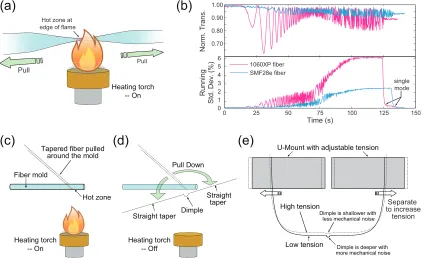
Taper Pulling and Molding
to trigger the end of the pull.1 To produce tapers with the desired length (∼1 cm for the region withd.10µm) and minimum diameter (∼1µm), typical pulls continue ∼10 s after the oscillations stop and take 120–150 s with the stages each moving at ∼1.5 cm/min, but there is significant variability depending on how the fiber is prepared. For instance, the single-mode jump in the running standard deviation will contain one or more discrete steps if the fiber is subjected to undue stress while the polymer coating is being removed.
After mounting the taper in a U-bracket [104], the narrowest part of the taper is pressed against a silica mold with the desired radius of curvature [Fig. 2.1(c)]; a bare optical fiber with a diameter of approximately 125µm is used as the mold in these experiments. The taper and mold are heated with a hydrogen torch and allowed to cool. To detach the taper from the mold, we simply pull the taper away slowly while moving it back and forth (i.e., we are inducing fatigue failure at the taper-mold joint). A thin layer of soot on the mold improves the detachment yield—an appropriate layer is usually deposited when the torch is sparked.2 After releasing the fiber from the mold, the taper retains an impression of the mold, Fig 2.2(b), which forms a global minimum with respect to the rest of the taper. The dimpling process introduces negligible additional loss, and the total loss of the dimpled taper can be less than 0.5 dB relative to the unpulled optical fiber. However, tapers typically exhibit a total loss 1–2 dB. Using a specially designed U-mount with a set screw to control the tensioning, varying the taper’s tension changes the radius of curvature of the dimple. Under high tension, the dimple becomes very shallow but never completely straightens. After dimpling, the probe is mounted onto a three-axis 50-nm encoded stage and is fusion spliced into a versatile fiber-optic setup. During testing, devices are placed in the near field of the probe, as in Fig. 2.2(a,c); adjustments to a pair of goniometers ensure the straight run of the taper is parallel to the sample surface.
Measurement of the non-resonant insertion loss as the waveguide is moved relative to nearby semiconductor microstructures gives the effective interaction length and profile of the local probe. First, we record the loss as a 1.6-µm wide GaAs cantilever is scanned along the taper’s length (ˆx-direction) while holding the taper at a fixed height. At tensions used in standard testing, Fig. 2.3(a) shows only ∼20µm (full width at half maximum) of the taper
1This method was implemented by C. Chrystal. A similar procedure has been published by F. Orucevic
et al. using a running Fourier transform [103].
2N.B. Do not spark H
2 torches near the fiber either before or after tapering as it will significantly reduce
5 μm
50 μm
20 μm
Figure 2.2: (a) Illustration of a “dimpled” taper coupled to an undercut microdisk. (b) Optical image of the taper probe. The taper diameter at the center of the dimple is∼1.2µm. (c) At the center of a 5×5 array, the dimpled taper probe is critically coupled to the microdisk at the center of the array but not coupled to any of the neighboring disks.
at the bottom of the dimple is close enough to interact with the sample. Second, the loss is measured as a function of the probe’s height (ˆz-direction) above a 11.6-µm wide GaAs mesa. By assuming an exponential vertical dependence for the insertion lossL∝e−zt(x)/zo
where zt(x) is the probe’s “near-field” profile and zo is the decay length from Fig. 2.3(b), we convert the axial dependence of the loss [Fig. 2.3(a)] into zt(x) [Fig. 2.3(c)]—i.e., the height of the taper relative to the lowest point of the dimple. Since only the lowest part of the dimple interacts with the sample, this method can only determine the taper’s profile within∼1.25µm of the surface. Fitting the profiles determines the effective probe radius to be 159, 228, and 498µm at low, medium, and high tension, respectively. These radii differ from the mold radius (∼62µm) due to tensioning of the taper and how the fiber detaches from the mold after heating.
2.2
Microphotonic Testing with a Dimple-Taper Waveguide
losses by absorption at the first overtone of the OH− vibrational modes [105, 106].3 The HE11 mode of the taper is excited using fiber-coupled swept tunable-laser sources (span-ning 963–993 nm and 1420–1625 nm, linewidth of <300 kHz over the 25-ms timescale used to scan across a high-Qresonance) and a paddle-wheel polarization controller to selectively couple to the cavity’s TE-like and TM-like WGMs. To accurately measure the intrinsic quality factor, the cavities are weakly loaded by the dimpled probe to ensure the extrinsic loading is negligible (γe≈0) and avoid any parasitic coupling. Two complementary VOAs are used to maintain a constant optical power at the photodetector (to give a constant electronic noise level) while power at the device can be varied up to 60 dB [107]. To elimi-nate any nonlinear effects or absorption saturation while acquiring the transmission spectra, the lasers are usually attenuated to give ∼200 nW at the taper, of which∼10% is coupled into the microdisk cavity. Without any optical amplification, the signal is detected using a high-speed InGaAs photodiode, electrically amplified using a low-noise analog preamplifier, and then is aquired by a analog-to-digital converter. For narrow spectral features (e.g.,
Q >106 corresponds toδλ.1.5 pm), the linewidth measurement can be calibrated with a fiber-optic Mach-Zehnder interferometer to an accuracy of±0.02% (see also §A.1).
2.2.1 Noise Measurements
Because evanescent coupling to tapers is exponentially dependent on position, fiber-taper measurements are very susceptible to any noise sources that produce physical dis-placements of the taper. For straight tapers, increasing tension to reduce these fluctuations is common, and the U-mount [104] naturally provides the appropriate tautness. Under standard testing conditions at low dimple-taper tension [Fig. 2.5(a)], coupling to the mode of a microdisk resonator [see Fig. 2.2(a) and §2.2.2] varies significantly between consecu-tive scans. Increasing the tension makes the coupling depth much more reproducible, as in Fig. 2.5(b). At tensions that give acceptable noise levels, the depth of the dimple is still adequate for testing densely spaced planar devices.
To quantitatively study the noise, we measure non-resonant insertion loss as a function of time. The dimple is placed above the etched GaAs mesa so that approximately 60% of the incident power is coupled into the substrate [z ≈ 170 nm as in Fig. 2.3(b)]. The
3After months of use in a N
2 box, enough water and dust will accumulate to significantly reduce the
indicate optical forces can statically deflect the dimple up to 200 nm for 600µW of power coupled into the cavity mode. Even with lower-Q optical resonances (Q ≈ 102), optical forces from similar amounts of dropped power can drive mechanical oscillations with am-plitudes of∼500 nm. These results are discussed in detail elsewhere [108].
2.2.2 Dense Si Microdisk Array
To demonstrate the dimpled taper’s ability to test closely spaced devices, we study a 5×5 array of silicon microdisks [Fig. 2.2(c)] with disk diameters of 10µm and periodicity of 20µm—corresponding to an areal density of 2.5×105cm−2. Undercut microdisks were cho-sen over planar resonators to ease phase matching between the cavity and taper modes. The microdisks were fabricated from silicon-on-insulator with a 217-nm device layer [h100i orientation, p-type, 14–20 Ω·cm] and a 2-µm SiO2 buried oxide layer (BOX). The resonators were defined using electron-beam lithography, resist reflow, and C4F8:SF6 reactive ion etch-ing (RIE); then the disks were partially undercut by etchetch-ing the buried oxide usetch-ing dilute HF. The silicon surfaces are temporarily hydrogen passivated using repeated Piranha/HF treatments. Long-term passivation is achieved using a 3-nm dry thermal oxide cap grown in O2 at 1000◦C followed by a 3-hour anneal in N2 at 1000◦C and then a 1.5-hour slow cool down in N2from 1000◦C to 400◦C. For details on the lithography, chemical passivation, and oxide passivation, see Refs. [42], [56], and [109], respectively.
Near 1532 nm, we track three TE-like modes of different radial orders [p = 1–3 in Fig. 2.6(a)] across all 25 disks in the array. One disk supported no high-Qwhispering-gallery modes in the range spanning 1495–1565 nm, and we were unable to couple to the TEp= 1 mode in two other disks—most likely because their Q was too low to overcome the phase mismatch with the taper mode. In Fig. 2.6(b), varying the disk-taper coupling through their separation practically demonstrates the level of displacement noise present in these measurements; each circle represents the transmission minimum for an individual scan at the given probe position. Table 2.1 summarizes the average measured wavelength (λo), quality factor, and doublet splitting (∆λ) for each mode; the distributions of wavelength and quality factor4 appear in Fig. 2.6(a). The highestQfor a single standing wave mode is 3.3×10⁶with
Q/Veff = 2.3×10⁵ for a calculated mode volume Veff = 14.09 (λ/n)3. With minimal free-4For doublet modes, the quality factor used in Fig. 2.6(c) is the averageQbetween the two standing-wave
-4 -3 -2 -1 0 1 2 3 4 0.980
0.984 0.988 0.992 0.996 1.000
Wavelength (pm)
Normalized T
ransmission δλ = 0.35pm
δλ = 0.30pm
a)
b)
c)
Q = 4.1x10⁶
Q = 4.8x10⁶ 20 μm
200 nm
Figure 2.7: SEM images of rings after the final chemical treatments and 30-nm thermal oxidation: (a) top-view of a ring with a 20-µm diameter and 2-µm width and (b) side view showing smooth ring sidewalls and a slight BOX undercut due to the final chemical treatments. (c) Transmission spectrum of a high-Qmode at λo= 1428.7 nm in a ring with an 80-µm diameter and a 2-µm width.
2.2.3 Planar Si-SiO2 Microring via RIE Processing
Testing planar devices is accomplished in the same fashion. Non-undercut microring res-onators, shown in Fig. 2.7(a), were fabricated from SOI with a 195-nm silicon device layer and a 3-µm BOX. The same lithography, resist reflow, and RIE procedure used for the microdisks [42] was used to define the microrings although without the final HF undercut. Repeated Piranha oxidations and HF dips are again used to chemically passivate the sur-faces prior to thermal oxidation [56]; these treatments also slightly undercut the resonators [Fig. 2.7(b)]. Finally, a 30-nm dry thermal oxide was grown as a capping layer, and the microring sample was annealed according to the same N2 schedule as the microdisks [109]. Microrings are slightly more difficult to test with fiber-tapers than undercut microdisks. A large phase mismatch exists between the taper and microcavity because of the extra dielectric beneath the Si-core guided modes. With the taper in contact with the ring, the coupling depth is more than sufficient to assess the devices’ optical loss characteristics. However, the coupling is not adequate to efficiently excite and collect emission from active devices [70]. For applications requiring high pump/collection efficiency, photonic crystal waveguides can be used to overcome the poor phase matching between the modes in the taper and the modes in the on-chip device [77].
Figure 2.7(c) shows a transmission spectrum of a ring with an 80-µm diameter and
factor of 4.8×10⁶ (loss coefficient α < 0.15 dB/cm) represents the highest quality factor for any planar microresonator to date. ReproducingQs found previously only in relatively thick and undercut silicon disks [42] is promising for the future development of PLCs with high-Q silicon microresonators integrated with bus waveguides.
2.2.4 Planar Si-SiO2 Microring via LOCOS Processing
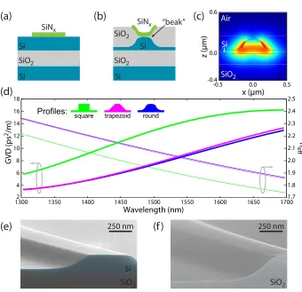
Wet chemical oxidation of ridge waveguides has been used to smooth silicon surfaces and reduce Rayleigh scattering [111]. However, similar treatments of high-Qmicrodisks did not reduce the scattering rate but rather increased the measurable loss by introducing unpas-sivated mid-gap surface states [56]. As evident by the contradictory results for chemical oxides, significant care must be taken in low-loss fabrication procedures. Dry reactive-ion chemistries are generally preferred over wet chemical etchants because they are more anisotropic, but RIE recipes must be carefully optimized for roughness and can damage the surface (chemically and physically). Two alternatives have been to use shallow rib waveguides, in which the modes are weakly guided and have minimal overlap with the sur-faces [112], or to use a diffusion-limited chemical reaction to produce the cladding layer [113]. In the latter case, dry thermal oxidation of Si device layer in SOI produces a low-loss SiO2 cladding with a well-passivated interface [109] and high refractive index contrast to the underlying Si core. This section describes initial results for the fabrication and dispersion engineering of submicron waveguides formed by the local oxidation of silicon (LOCOS).
With the ultimate objective of achieving CW parametric oscillation in a Si microcavity, the final devices must be high Q, have a small group velocity dispersion (GVD) with a zero-dispersion wavelength (ZDWL) near the desired wavelength, and exhibit a low free-carrier lifetime (τfc). Degenerate four-wave mixing can be used to generate broadband gain in silicon microphotonics because of its largeχ3nonlinearity [114], but the modal dispersion must be controlled to ensure phase matching. In WGM resonators, the phase matching is trivially satisfied between consecutive modes in a single family, but the GVD must be near zero to converse energy (i.e., the signal and idler modes must be equally spaced about the pump mode) [115]. An additional constraint when operating with a photon energy above half the material’s bandgap is thatτfcmust be short to minimize absorption by e−/h+pairs generated by two-photon excitation.
(a)
1300 1350 1400 1450 1500 1550 1600 1650 1700
rounds the Si profile at the edges [Fig. 2.8(b)]. Since the resulting “bird beak” contour may not be accurately captured by effective-index methods, the waveguide modes and disper-sion are evaluated using the FEM. The effective-index requirement limits the geometries to submicron dimensions that cut off all but the TEp=1 mode [Fig. 2.8(c)]—TM modes will be avoided initially because of lateral leakage into the partially thinned slab [26]. Prelimi-nary simulations show the dispersion can be flattened by modifying the waveguide profile [Fig. 2.8(d)], but the GVD for modes with these dimensions may never reach zero in the telecommunications windows. Smaller Si structures having greater overlap with the BOX or a SiO2 cap will have a lower GVD because silica is anomalous in this range. To proceed, we target a waveguide width of 230 nm, Si thickness of 210 nm, and a ridge height of 160 nm with nwgeff = 2.02 at λo = 1550 nm. While ring resonators with these dimensions have sig-nificant +GVD at 1550 nm, they are an acceptable starting point for process development. Future devices may utilize the TMp=1 modes to simultaneously achieve the neff and GVD objectives while demanding greater pattern control (i.e., waveguide width).
The process begins by using Piranha etch (3:1 concentrated H2SO4 to 30% H2O2) to remove any residual organics on a SOI wafer (217 nm Si, 2µm BOX). After a quick HF rinse to strip the native oxide, a 10-nm dry thermal oxide is grown at 1000◦C to serve as an etch-stop layer and protect the Si surface. A 75-nm low-stress SiNx mask is then deposited by plasma-enhanced chemical vapor deposition (PECVD). This layer must be thick enough to provide an adequate diffusion barrier, but it must be compliant (thin) enough to not delaminate as the SiO2 expands [Fig. 2.8(b)]. The nitride is then patterned with electron-beam lithography, resist reflow, and RIE (C4F8:SF6). Since the selectivity between SiNx and SiO2is poor, the etch must be carefully timed to stop at the etch-stop layer. Following another Piranha clean to take off any remaining resist and etch by-products, the sample is oxidized in dry O2 (electronic grade II) at 1100◦C to define the waveguides. The SiO2 and SiNx are then removed with HF leaving the Si surface bare for future surface treatments.
dimensions must be calibrated against the resulting widths to account for the resist reflow and SiNx sidewall angle, which is not perfectly vertical. Even after correcting for lateral diffusion that will undercut the SiNxby the same depth the sample is oxidized (e.g., oxidizing down 160 nm to define a 230-nm waveguide requires a mask width of ∼550 nm), the final waveguides were too large (∼500 nm) for testing with a dimple taper. Third, the long LOCOS oxidation anneals the PECVD SiNx and increases its resistance to HF. Instead of being etched during the final HF strip, the SiNx lifts off in one large sheet as the thin SiO2 etch-stop is slowly undercut. Much of surface roughness on top of the waveguides is likely due to the SiNx gradually pealing off the Si. In addition, the longer etch allows HF to penetrate defects in the silicon/oxide layers and partially undercut the BOX layer; it is uncertain whether these defects are process induced or are intrinsic to the Si layer in the original SOI wafer. A thicker SiO2etch barrier will also ameliorate these issues by expediting the liftoff. To test ring resonators from this initial run, we partially oxidize the samples to reduce neff—the waveguide now consist of a smaller Si core with a SiO2 cladding. These Si-SiO2 rings have Q ≈ 1–2×10⁵ (3.6–7.2 dB/cm) and no measurable doublet splitting. Further oxidation completely consumes the Si core, but physical inspection in Fig. 2.8(f) shows the surface roughness is reduced similar to the chemical oxidation in Ref. [111]. These preliminary results along with recent reports [118,119] show the potential for achieving low-loss dispersion-engineered Si-SiO2 microrings using LOCOS processing.
2.3
Conclusions
Chapter 3
Linear Absorption in AlGaAs and
GaAs Microcavities
In recent semiconductor cavity QED experiments involving self-assembled III-V quantum dots (QDs), Rabi splitting of the spontaneous emission line from individual QD excitonic states has been measured for the first time [121–123]. Potential application of these devices to quantum networks [124] and cryptography [125] over long-haul silica fibers has sparked interest in developing QD-cavity systems with efficient light extraction operating in the telecommunication bands at 1300 and 1550 nm [126]. The initial demonstrations of vacuum-Rabi splitting in this system, a result of coupling a single QD to localized optical modes of a surrounding microresonator, have been greatly aided by prior improvements to the design and fabrication of semiconductor microcavities [23, 127, 128]. At the shorter wavelengths involved in these Rabi splitting experiments (740–1200 nm), the optical quality factors (Q) of the host AlGaAs microcavities were limited to Q≈2×10⁴—corresponding to a loss rate comparable with the coherent QD-cavity coupling rate. Further reduction of optical loss would increase the relative coherence of the QD-cavity system and would allow greater coupling efficiency to the cavity mode.
character-ize losses due to material absorption and surface scattering [42, 56, 69]. In this chapter1 we study the properties of GaAs and Al0.18Ga0.82As microdisks across three wavelength bands centered at 980, 1460, and 1600 nm. After estimating and removing the surface-scattering contribution to the cavities losses, we find the remaining absorption, composed of losses in the bulk and on the surfaces, depends significantly on both wavelength and material composition.
3.1
Al
xGa
1−xAs Samples and Processing
The samples were fabricated from high-quality heterostructures grown by molecular beam epitaxy (MBE) on a GaAs substrate. Two different samples were grown: a “GaAs” sample containing a 247-nm GaAs disk layer, and an “AlGaAs” sample with a 237-nm Al0.18Ga0.82As disk layer. In both samples the disk layer was grown nominally undoped (background doping levels np . 1015cm−3) and was deposited on a 1.6-µm Al0.7Ga0.3As sacrificial layer. Microdisks with a radius of∼3.4µm were defined by electron-beam lithog-raphy and etched in a 55 percent (by volume) HBr solution containing 3.6 g of K2Cr2O7 per litre [131]. The disks were partially undercut by etching the sacrificial layer in 8 percent HF acid for 45 s, prior to e-beam resist removal.
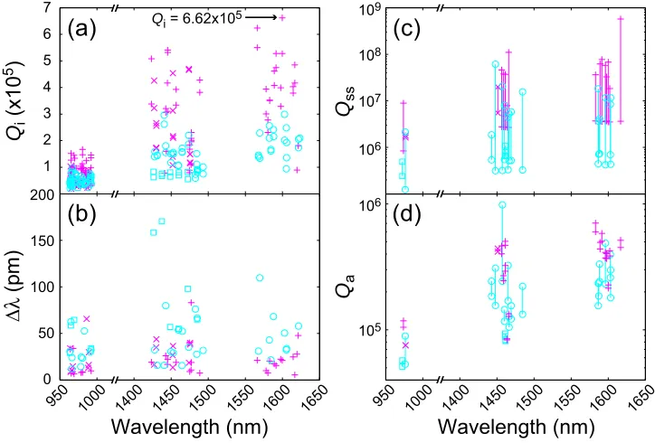
The measured Qis for all observed modes are summarized in Fig. 3.2(a); each family of modes is identified by comparing the coupling behavior and free spectral range to FEM models [56]. Modes with Qis dominated by radiation loss, i.e., the measured Qi is near
Qrad calculated using FEM simulations, are omitted. For all the microdisk modes in these measurements, the calculatedQrad is&106 and typically is>108. In the 1600-nm band, the high-QTE modes arep= 1–4 in GaAs andp= 1–3 in AlGaAs; all TM modes are radiation limited in this band. Near 1460 nm, the TEp=1−4 and TMp=1 modes in both materials are detectable and not radiation limited. In the 980-nm range, identifying modes becomes more difficult: at this wavelength families through TEp=8 and TMp=7 are not radiation limited, and significant spectral overlap between the modes causes Fano-like resonance features [71]. In addition, we are unable to couple to the lowest order modes of both polarizations (p≈
1–3) because they are poorly phase matched to the fiber-taper.
1Reprinted with permission from Appl. Phys. Lett.90, 051108 (2007). Copyright 2007, American
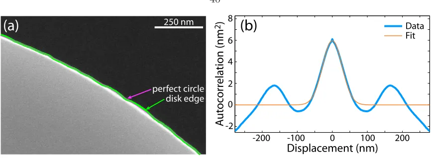
200 nm 200 nm
950 1000 1400 1450 1500 1550 1600 1650
0
950 1000 1400 1450 1500 1550 1600 1650
dominant bulk absorption in the GaAs disks. In the 980-nm band, the data is consistent with bulk absorption [γa,TM/γa,TE= 1.05±0.40 (1.39±0.66) for the AlGaAs (GaAs) devices] although the results are less conclusive due to the larger scatter in the data.
In summary, after accounting for radiation and surface scattering losses, we measure greater sub-bandgap absorption in Al0.18Ga0.82As microdisks than in similar GaAs res-onators, and the absorption in both materials decreases toward longer wavelengths. This finding is at least partially reflected in recent cQED experiments with a single QD near or in the strong-coupling regime [121–123, 135–142] that show the longest cavity photon life-times (τph ≈70 ps) are achieved in devices at longer wavelengths (λo = 1294.5 nm) [138].3 From the polarization dependence of the measured optical loss, we infer that both surface states and bulk states contribute to the residual absorption in these structures. Our results imply that reductions in the optical loss of AlGaAs-based microphotonics, especially at the shorter wavelengths of<1µm and in high Al content alloys, will require further study and reduction of deep level traps, and that surface passivation techniques [143, 144] will also likely be important.
3Longer cavity lifetimes (τ
ph ≈ 80 ps at λo = 940.5 nm) have been demonstrated in large AlAs/GaAs
Chapter 4
Optical Processes in
Epitaxial c-Er
2
O
3
on Silicon
Significant progress in the last decade has been made developing passive and active silicon optical components; however, efficient generation of light within a Si platform remains a technical and commercial challenge [79]. Efforts to incorporate Er3+ into the Si material system, with erbium’s emission in the 1550-nm telecommunications band, have met with limited success. Amorphous Er3+-doped glass waveguides on Si provide insufficient gain (<4 dB/cm [145, 146]) for dense photonic integration, while doped silicon allotropes are limited by other effects such as Auger recombination [147] and free-carrier absorption [148]. Here we describe the characterization of stoichiometric single-crystal Er2O3 grown on Si by atomic layer epitaxy (ALE).1 We measure a peak resonant absorption of 364 dB/cm at 1535 nm, negligible background absorption (<3 dB/cm), and strong cavity-polariton ef-fects. The observed radiative efficiency from 1520 to 1650 nm is 0.09% with cooperative upconversion producing strong green and red emission for Er3+ excitation levels as low as 2%.
Spurred by the growing power consumption of high-speed electrical interconnects for multicore processors [149,150], optical networks have become an attractive option to achieve Tb/s on-chip bandwidth [120,151,152]. Following the initial demonstration of silicon waveg-uide devices [153], there has been significant development in adding optical functionality to silicon microelectronics and, similarly, applying the efficiency and infrastructure of mod-ern complementary metal-oxide-semiconductor (CMOS) processing to optical telecommu-nication components. While silicon exhibits low loss across the 1300-nm and 1550-nm
1This work was done in collaboration with Translucent, Inc., where these epitaxial rare-earth oxide films
telecommunication windows, unstrained silicon lacks any significant Pockels coefficient and produces little emission from its 1.1 eV indirect bandgap [79]. Free-carrier dispersion and four-wave mixing provide some inherent active functionality, such as modulation with rates exceeding 1 GHz [154] and wavelength conversion [114], but considerable research, especially concerning light emission and detection, has focused on integrating silicon with other optical materials such as SiGe [155, 156] and the III-Vs [157, 158]. In this chapter we describe the growth, processing, and optical properties of c-Er2O3 films on Si. Similar to stoichiomet-ric polycrystalline Er3+ materials [159–164], Er
2O3 allows for a 100-fold increase in Er3+ concentration over conventional Er-doped glasses [165], making it an attractive material for on-chip emission and amplification in the 1550-nm wavelength band
![Figure 1.3: Comparison of the eigenvalues (ko) found using effective-index and finite-elementmodels for (a) TE modes in a Er2O3 disk and (b) TM modes in a Si disk plotted againstfree-space wavelength [λo = 2π/ℜ(ko)]](https://thumb-us.123doks.com/thumbv2/123dok_us/1053482.1131698/26.612.172.475.193.521/figure-comparison-eigenvalues-eective-nite-elementmodels-againstfree-wavelength.webp)