Design and Analysis of a New Soft-Switching
Multi-Output Fly-Back Converter
M.Ajith Kumar
1, N.Bhaskara Rao
2M. Tech Scholar [PEED], Dept. of EEE, Gudlavalleru Engineering College, Gudlavalleru, Andhra Pradesh, India1
Assistant professor, Dept. of EEE, Gudlavalleru Engineering College, Gudlavalleru, Andhra Pradesh, India2
ABSTRACT:This paper presents a new multi output converter. Demand for multiple output power supplies with low
voltage and high current has increased. A multi output converters needs to satisfy these conditions such as efficiency, voltage regulation, isolation and size. The fly back converter is the most attractive because of its relative simplicity compared with other topologies used in low power applications and we get multiple outputs. The proposed fly back converter operated at zero-voltage-switching (ZVS) turn-on and zero-current-switching (ZCS) turn-off process. The operational principle, analysis, and design considerations of the proposed converter are presented in this paper.
KEYWORDS: Fly-back converter, Multi output, Zero Current Switching [ZCS], Zero Voltage Switching [ZVS].
I.INTRODUCTION
The Utilization demand for multiple-output power supplies with low voltage and high current has increased [1] – [5], specifically in medical application that is therapeutic ultrasound. A multi-output converter needs to satisfy these conditions such as high efficiency at any load condition, voltage regulation, isolation and compact size. The Fly-back topology is the most attractive because of its relative simplicity compared with other topologies used in low power applications and we can easily achieve multiple outputs. The high frequency Fly-back transformer [6] serves the dual purpose of providing energy storage as well as converter isolation and minimizing the magnetic component count when compared with the forward converter. The Conventional Fly-back converter has found to be suitable for low input voltage and low-medium-power applications.
In recently many of the soft switching techniques are developed [7]-[14]. The soft switching schemes [7]-[8] with variable switching frequency have been proposes to reduce the size of power converters and switching losses on power semiconductors. The many techniques were developed in [9]- [11] to achieve zero voltage switching, and zero current switching [12]-[14] turn-on. In half bridge fly-back converter proposed in [5] [10] the voltage across the switches is not greater than the input voltage, causing the short circuit of the auxiliary switch snubber capacitor during turn on. The switch current is limited by only it’s on state resistance, which would damage the switch during turn on due to the flow of large current at the instant of turn on.
buck converters for the auxiliary outputs.
The proposed converter integrated with the secondary fly back rectifier. This integration makes simple structure, and lower transformer size, and of main switch is operates at zero voltage- switching turn-on and zero-current-switching turn-off condition are achieved to gate control without additional components. In addition, cross regulation problems among the outputs do not occur.The auxiliary switch and the other semiconductor devices are operate at zero-current-switching turn-on and turn-off condition. The principle of operation, theoretical analysis of the proposed multi-output Fly-back converter rated 130W and operating at 100 kHz, provided to verify its performance.
II
.
PRICIPLE OF OPERATIONIn conventional circuit have the two outputs and two switches in the both fly back converter and transformer secondary side which causes additional losses the operation is divided into six modes. The main operation for the both conventional and proposed operated one on duty cycle D and other one is compliment to it of the primary side. On the secondary side switches are removed and transformer turns are increased to get the multiple outputs.
1 Fig.2: Conventional Fly back converter with two outputs
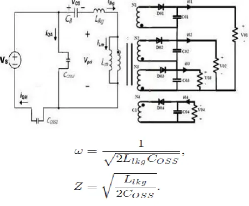
The proposed multi output Fly-back converter shown in Fig.3. The circuit can divided in two parts. The first part is a conventional Fly-back converter, which is responsible for power transferred into the load. It is composed of an isolated Multi-winding transformer, a main switch Qm, output diodes D01, D02, D03& D04, and output filter C01, C02, C03 & C04. The Second part is commutation cell to provide the ZVS-ZCS to the main switch Qm. It is composed of the resonant inductor L1kg, the resonant capacitor CB, and auxiliary switch Qa, This section provides the soft-commutation functions to the power semiconductor devices of the Fly-back Converter.
Fig.3: Block diagram of proposed Multi output Fly back converter
Operating modes and analysis:
Mode 1[to-t1]: Mode 1 begins when S1 is ON S2 is OFF current flows from Switch S1 to primary of transformer.
During this mode diodes D01, D02, D03and D04 are forward biased.
Ws= and Ceq=
Mode 2[t1-t2]: During this Mode Switch S1 is OFF S2 is ON the diodes D01, D02, D03and D04 are reverse biased.
Ws= and Ceq=
Mode 3[t2-t3]: During Mode 3 both S1 and S2 is turned OFF current stored by magnetizing inductor is discharged
through primary wining of transformer. Due to this the diodes D01, D02, D03and D04 are forward biased.
III.DESIGN CONSIDERATIONS
The gating signals for the primary side switches of the converter are given below which operate system correctly.
Fig 5.Gate Signals S1 & S2 of Proposed Converter
A. Design of voltage Transformer Ratio:
The turn’s ratio design of proposed converter is similar to the conventional Fly-back converter. The transformer voltages ratios are 1:N1, 1:N2, 1:N3, 1:N4. The turn’s ratio can calculated as follows.
B. Design of transformer magnetizing inductance:
The Fly-back transformer magnetizing inductance design is similar to the traditional Fly-back converter and can be calculated as follows
Where R0 is the total equivalent resistance referred to primary side of transformer R '0 =N2R0
C. Design of output filter capacitance:
Design of the output filter capacitor is based on the output Voltage ripples specifications.
Where ⧍V is the peak – peak ripple voltage ac component of the voltage across the capacitor.
D. Design of resonant components:
The inductance Ls is selected maximum value of the current through it.
IV.SIMULATION RESULTS
The simulation results are shown in Fig.3. The specification of the converter is 100 KHz switching frequency. The main switch is turn on under ZVS and turn off under ZCS condition. The auxiliary switch and other semiconductor devices are operated under ZCS condition are shown in Fig.3.
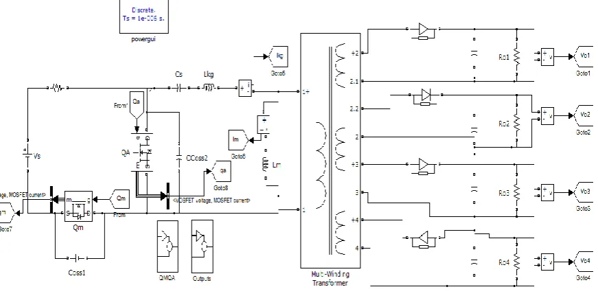
Fig 6 Matlab/Simulink Diagram
Fig 6 shows the simulink diagram of the proposed topology in which ZCS-ZVS is used for Turn ON-Turn OFF purpose and switches are eliminated.
Fig 7. S1 &S2 Control Circuit of Proposed Converter
Fig 8.Apply ZVS on S1 & S2 switches of Proposed Converter
Fig 8 gives the information about the Zero Voltage Switching (ZVS) operation of the circuit which shows the current is going to vary linearly when the voltage is off condition.
Fig 9.Apply ZCS on S1 & S2 switches of Proposed Converter
Fig 9 gives the information about the Zero Current Switching (ZCS) operation of the circuit which shows the Voltage is going to vary linearly when the Current is off condition.
Fig 10.Transformer Primary Voltage
Fig 10 transformer primary winding voltage of the proposed circuit which is going to supplied to the system and operation depends on the switches turn on and off condition.
Fig 11.Leakage Current of Inductor
Fig 11 leakage currents of the proposed topology in which losses are going to reduced in its value when compared to
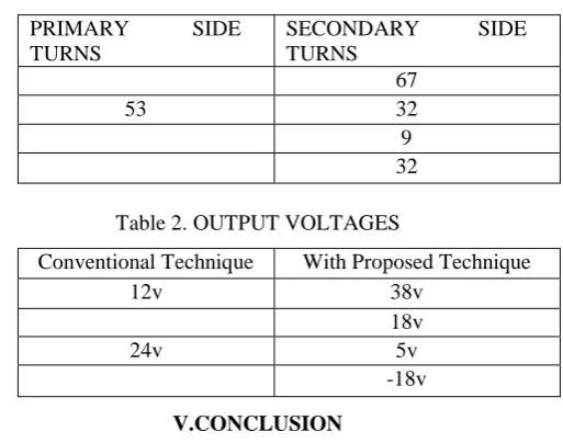
53 32 9 32
Table 2. OUTPUT VOLTAGES
Conventional Technique With Proposed Technique
12v 38v
18v
24v 5v
-18v
V.CONCLUSION
This paper presents a Complete simulation of Fly back converter with ZVS-ZCS is achieved for all the switches by gate control without additional components to get the multiple outputs. High efficiency is obtained under entire load conditions with reduced switching stress because secondary side switches are eliminated. No cross regulation problems occur. The proposed converter is suitable for multi output power supply which requires the outputs with same ground.
REFERENCES
[1] Jae-Kuk Kim, Jae-Bum Lee, Student Member, IEEE, and Gun-Woo Moon, Member, IEEE.
[2] Y. Jang and M. M. Jovanovic, “Light-load efficiency optimization method,” IEEE Trans. Power Electron., vol. 25, no. 1, pp. 67–74, Jan.2010. [3] H. S.-H. Chung, S. Y. Hui, and W.-H. Wang, “A zero-current-switching PWM flyback converter with a simple auxiliary switch,” IEEE Trans.
Power Electron., vol. 14, no. 2, pp. 329–342, Mar. 1999.
[4] C. Ji, M. Smith, Jr., K. M. Smedley, and K. King, “Cross regulation in flyback converters: Analytic model and solution,” IEEE Trans. Power Electron., vol. 16, no. 2, pp. 231–239, Mar. 2001.
[5] S.-Y. Cho, I.-O. Lee, J.-K. Kim, and G.-W. Moon, “A new standby structure based on a forward converter integrated with a phase-shift full-bridge converter for server power supplies,” IEEE Trans. Power Electron., vol. 28,no. 1, pp. 336–346, Jan. 2013.
[6] Q. Chen, M. M. Jovanovic, and F. C. Lee, “Analysis and Design of Weighted Voltage-Mode Control for a Multiple-Output Forward Converters,” Applied Power Electronics Conf, Mar. 1993 pp. 449- 455, .
[7] L. K. Kaushik, and M. K. Pathak, “An improved multiple output forward Converter topology,” Int. Conference on Power Electronics and Drives Energy Syst., 2010, pp. 1–6.,
[8] H.S. Kim, J.H. Jung, J.W. Baek, and H.J. Kim, “Analysis and Design of a Multioutput Converter Using Asymmetrical PWM Half-Bridge FlybackConverter Employing a Parallel–Series Transformer,” IEEE Trans.on Industrial Electronics, vol. 60, pp.3115-3125, Aug 2013 [9] O.Garcia, J.A. cobos, P. Alou, R.Prieto, and J.Uceda, “A simple single switch single-stage ac/dc converter with fast output voltage regulation,”
IEEE Trans. Power Electron., vol 17, pp. 163– 171, 2002
[10] C.A.canesin., and I.Barbi, “Novel zero-current-switching PWM converters,” IEEE Trans. Ind. Electron., vol 44, pp. 372– 381, 1997. [11] G.hua, and F.C.lee, “Soft-switching techniques in PWM converters,” IEEE Trans. Ind. Electron., vol. 42, pp. 595– 603, 1995.
[12] T. M. Chen and C.-L. Chen, “Analysis and design of asymmetrical half bridge Fly-back converter,” IEE Proc. in Elect. Power Appl, vol. 1, pp. 433–440. Nov. 2002
[13] J.-H. Jung, and J.-G. Kwon, “Soft switching and optimal resonance conditions of APWM HB Fly-back converter for high efficiency under high output current,” IEEE conference PESC, 2008, pp. 2994–3000.
[14] B.R. Lin, and J. J. Chen, “Analysis of an integrated Fly-back and zeta converter with active clamping technique,” IET Power Electronics., vol. 2, pp. 355–363, May 2009.
[15] H. S. H Chung, S. Y. Hui, and Wei-Hua Wang, “A Zero-Current- Switching PWM Fly-back Converter with a Simple Auxiliary Switch,” IEEE Trans. on power electronics, vol. 14, pp.329-342 Mar 1999
[16] C. M. Wang, “A Novel ZCS-PWM Fly-back converter with simple ZCS-PWM commutation cell,” IEEE Trans. Ind. Electron., vol. 55, pp. 749-757, Feb. 2008.