ISSN (Print) : 2320 – 3765 ISSN (Online): 2278 – 8875
I
nternational
J
ournal of
A
dvanced
R
esearch in
E
lectrical,
E
lectronics and
I
nstrumentation
E
ngineering
(An ISO 3297: 2007 Certified Organization)
Vol. 5, Issue 2, February 2016
Realization of All-Optical Reversible Logic
Gates using Mach-Zehnder Interferometer
Arsha Renjan1, Gokul P G2
PG Student [OEC], Dept. of ECE, TKM Institute of Technology, Kollam, Kerala, India1 Assistant Professor, Dept. of ECE, TKM Institute of Technology, Kollam, Kerala, India2
ABSTRACT: With the advancements in all-optical computing technology, researchers have been paying more attention towards designing low-power applications. Reversible logic has promising applications in dissipation less optical computing, low power computing, quantum computing etc. A circuit is said to be reversible if the input vectors can be recovered from the output vectors and there is a one to one correspondence between its input and output assignments. Reversible logic circuits in optical domain will play a major role in designing power efficient, high speed optical networks. Mach-Zehnder interferometer (MZI) plays a significant role in the field of ultra fast optical computing, because of its features like high speed, fast switching time and ease of fabrication. There are number of universal reversible logic gates, i.e. any logical reversible circuit can be realized using these gates. Reversible logic gates like Toffoli gate and Peres gate are realized using optisystem software.
KEYWORDS: Mach-Zehnder interferometer (MZI),Optisystem, Peres Gate, Reversible logic,Toffoli Gate
I. INTRODUCTION
In conventional computers, the computation is irreversible i.e. once logic block generates the output bits, the input bits are lost[1]. The loss of one bit of information will lead to the kTln2 joules of energy, where k is the Boltzmann’s constant T is the absolute temperature. For a single bit, energy dissipation is very small. But in the case of high speed computational works more number of bits are lost, so the energy dissipation will be higher. Reversible logic is an alternative that allows computation with arbitrary small energy dissipation[2].
The conventional gates such as AND, OR and EXOR are irreversible as they have multiple input and single output. A gate is said to be reversible, if the gate's inputs can be recovered from the outputs, and one-to-one correspondence between input and output vectors[3]. Reversible logic gates must have an equal number of inputs and outputs.The unused outputs are used tomaintain the reversibility of reversible circuits are known as the garbage outputs. For performing certain logical operations some inputs are maintained as either 0 or 1. This constant inputs are known as
ancilla input/constant input.
All-optical logic for optical network is an exciting field ofresearch where much innovations can expect. Photons are the ultimate unit of information with unmatched speed and data package in a signal of zero mass. The all optical reversible gates are realized using Mach-Zehnder interferometer (MZI) because of its significant advantages such as high speed, low power, fast switching time and ease in fabrication.
II. MACH-ZEHNDER INTERFEROMETER (MZI)]
ISSN (Print) : 2320 – 3765 ISSN (Online): 2278 – 8875
I
nternational
J
ournal of
A
dvanced
R
esearch in
E
lectrical,
E
lectronics and
I
nstrumentation
E
ngineering
(An ISO 3297: 2007 Certified Organization)
Vol. 5, Issue 2, February 2016
cross port and no light at the bar port. In the absence of incoming signal at the input port A there is no light at both the output ports[5].
Fig.1 Mach-Zehnder interferometer based all optical switch
III. SYSTEM DESIGN
The basic reversible logic gates likeToffoli gate and Peres gate are realized using Mach-Zehnder Interferometer.
3.1 MZI based All-Optical Toffoli Gate
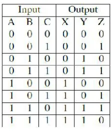
The Toffoli gate(TG) is a 3 * 3 reversible logic gate having A,B,C as input vectors and output vectors are X = A; Y = B;Z = AB C, where A, B, C are the inputs and X, Y, Z are the outputs. The logic symbol of Toffoli Gate is shown in the fig. 2.
Fig.2Logic symbol of Toffoli gate
The Toffoli gate can be realized using 3 MZI based all optical switches so the optical cost of Toffoli gate is considered as 3. The Toffoli gate has a delay of 2∆, because two MZI switches out of three MZI switches work in parallel.The truthtable is given in table 1.
Table 1
ISSN (Print) : 2320 – 3765 ISSN (Online): 2278 – 8875
I
nternational
J
ournal of
A
dvanced
R
esearch in
E
lectrical,
E
lectronics and
I
nstrumentation
E
ngineering
(An ISO 3297: 2007 Certified Organization)
Vol. 5, Issue 2, February 2016
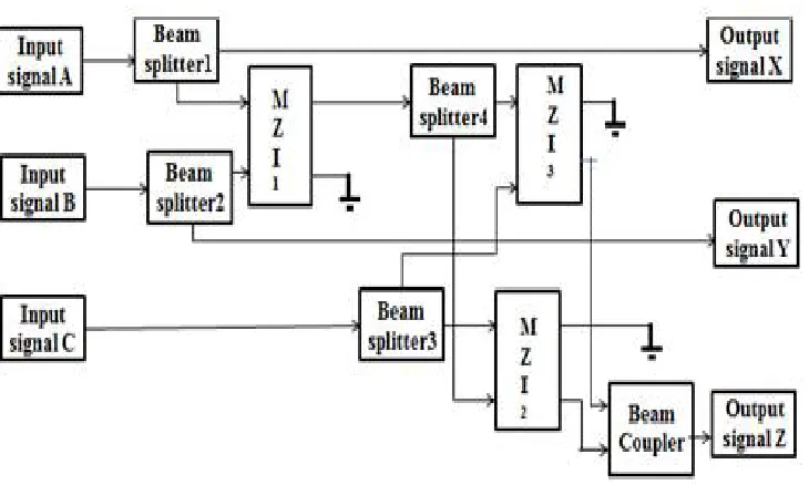
Fig. 3 shows all optical realization of Toffoli gate. When the value of input signal C is set to one, the Toffoli gate work as a NAND gate. An all optical Toffoligate can be realized using 3 MZI based all optical switches, 1 Beam coupler (BC) and 4 beam splitters. The input signals A and B are splitted into two optical beams byusing two beam splitters. One splittedoutputs of each beam splitters are directly taken as output X and output Y. Other splitted outputs are given to the input ports of first MZI. The bar port output of MZI is also splitted by another beam splitter. This splitted beams and input C are given to the two MZIs. The cross port outputs of two MZIs are given to the beam coupler . The beam coupler (BC) simply combines the optical beams. The output Z is taken from the beam coupler.
Fig.3 All optical implementation of Toffoli Gate
3.2 MZI based All-Optical Peres Gate
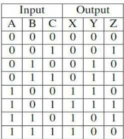
The Peres Gate is a 3*3 reversible logicgate having A,B,C as input vectors and output vectors are X = A; Y = A B;Z = AB C, where A, B, C are the inputs and X, Y, Z are the outputs. The logicsymbol of Toffoli Gate is shown in the fig.4.
ISSN (Print) : 2320 – 3765 ISSN (Online): 2278 – 8875
I
nternational
J
ournal of
A
dvanced
R
esearch in
E
lectrical,
E
lectronics and
I
nstrumentation
E
ngineering
(An ISO 3297: 2007 Certified Organization)
Vol. 5, Issue 2, February 2016
The Peres gate can be realized usingfour MZI based all optical switches so the optical cost of Peres gate is considered as 4. The Toffoli gate has a delay of 2∆,because two MZI switches work in series.The truthtable is given in table 2.
Table 2
Truth Table of Peres Gate
The circuit of all-optical MZI based Peres gate is shown in fig. 5. A Peres gate can be realized using 4 MZI based all optical switch, 3 beam coupler (BC) and 5 beam splitter (BS). The beam splitter is used to splitting the input signals into two optical beams which is given to the input ports of MZIs appropriately. The bar port and cross port outputs of MZIs are given to the beam coupler as per the output equations of Peres gate. The beam coupler (BC) is used to combining the optical beams.
Fig.5 All optical implementation of Peres Gate
IV. SIMULATION MODELLING
The proposed reversible logic gates such as Toffoli gate and Peres gate are simulated using Optisystem 12 software.
4.1 Simulation set up of Toffoli Gate
ISSN (Print) : 2320 – 3765 ISSN (Online): 2278 – 8875
I
nternational
J
ournal of
A
dvanced
R
esearch in
E
lectrical,
E
lectronics and
I
nstrumentation
E
ngineering
(An ISO 3297: 2007 Certified Organization)
Vol. 5, Issue 2, February 2016
optical time domain visualizer. The beam splitter is used to split the input signals. These signals are appropriately given as control signal and incoming signal of MZI switches. The first and second outputs are directly taken from the first and second inputs. Here the bar port outputs of MZI is splitted into two,this signal act asan incoming and control signals for MZI 3 and MZI 2 respectively. Then the cross port outputs of both MZI 2 and MZI 3 are combined using beam coupler. Finally the outputs of beam couplers are obtained as per the boolean expressions of the Toffoli Gate. Output signals are viewed through optical time domain visualizer.
Fig.6 Simulation diagram of Toffoli Gate
4.2 Simulation set up of Peres Gate
Simulation diagram of Peres Gate is shown in fig. 7. The two input binary datas are generated by using the user defined bit sequence generator. The frequency and power of the input signals be 193.1 THz and 1mW. The binary signals are converted into optical domain by using the optical gaussian pulse generator. Input signals are viewed through optical time domain visualizer. The beam splitter is used to split the input signals. These signals are appropriately given as control signal and incoming signal of MZI switch. The first output is directly taken from the first input. Then the cross port and bar port outputs are suitably combined using beam coupler. The first beam coupler combines the cross port output and bar port output of MZI 1. Similarly beam coupler 2 combines the cross port outputs of both MZI 1 and MZI 2 respectively. Then thecross port outputs of both MZI3 and MZI 4 are combined using beam coupler 3. Finally the outputs of beam combiners are obtained as per the boolean expressions of the Peres Gate. Output signals are viewed through optical time domain visualizer.
ISSN (Print) : 2320 – 3765 ISSN (Online): 2278 – 8875
I
nternational
J
ournal of
A
dvanced
R
esearch in
E
lectrical,
E
lectronics and
I
nstrumentation
E
ngineering
(An ISO 3297: 2007 Certified Organization)
Vol. 5, Issue 2, February 2016
V. RESULT AND DISCUSSION
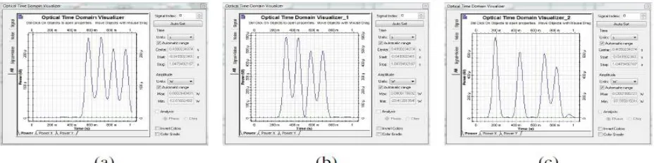
Toffoli Gate and Peres Gatehas three input signals. The simulated inputs are shown in the fig. 8. The optically generated inputs 00001111 , 00110011 and01010101 are viewed through the optical time domain visualizer.
Fig.8Simulated inputs of Toffoliand Peres Gate(a)Input(00001111), (b)Input(00110011),(c)Input(01010101) The Toffoli Gate generates three optical outputs. They are viewed through theoptical time domain visualizer. The simulated output signals 00001111 , 00110011 and 01010110 are shown in the fig.9. Hence the truth table of Toffoli Gate is verified.
Fig. 9Simulated outputs of Toffoli Gate(a)Output(00001111),(b)Output(00110011), (c)Output(01010110) The Peres Gate generates three optical outputs. They are viewed through the optical time domain visualizer. The simulated output signals 00001111 , 00111100 and 01010110 are shown in the fig. 10. Hence the truth table of Peres Gate isverified.
ISSN (Print) : 2320 – 3765 ISSN (Online): 2278 – 8875
I
nternational
J
ournal of
A
dvanced
R
esearch in
E
lectrical,
E
lectronics and
I
nstrumentation
E
ngineering
(An ISO 3297: 2007 Certified Organization)
Vol. 5, Issue 2, February 2016
VI.CONCLUSION
For future optical computing reversible logic gates are needed, as they have the potential of reducing power consumption. They have long-term benefits in the areas which require high energy efficiency, speed and performance. The basic reversible logic gates like Toffoli gate and Peres gate are realized using MZI switch. They can produce any boolean functions.
REFERENCES
[1] R.Landauer, “ Irreversibility and heat generation in the computational process”, IBM Journal of research and development, vol. 3, pp. 183-191, 1961.
[2]C.H Bennett, “ Logical Reversibility of Computation”, IBM J. Research and development, 17: pp. 525-532,November 1973.
[3]Deepak Pundir, Dr.Neena Gupta, “Study Of All-Optical Reversible Logic Gates”, International Journal of Computer Applications, April 2015. [4]KukiBordoloi, Shanthi Prince,T.Theresal, “Design Of All Optical Reversible Logic Gates”,IEEE International Conference on
Communication and Signal Processing, April 3-5, 2014.
[5] ChinmoyTaraphdar, JitendraNath Roy,TanayChattopadhyay, “MachZehnder interferometer-based all-optical reversible logic gate”, Elsevier, 2009.
[6] Ravi. H. N, Shilpakala. V,V. Kamalakannan, “ A Design Of Adder Subtractor Circuits Based On Reversible Gates ”, International Journal of Advanced Research in Electrical, Electronics and InstrumentationEngineering, Vol. 2, Issue 8, August 2013.
BIOGRAPHY
Arsha Renjan received her B.Tech degree in Electronics and Communication Engineering from University of Kerala in 2013. She is currently pursuing second year M.Tech in Optoelectronics and Communication Systems at TKM Institute of Technology.
Gokul P G received his B.E degree in Electronics and Communication Engineering from VTU
University, Karnataka in 2008 followed by M.Tech inDigital Electronics and Advanced