Fuzzy Logic Controller Based New
Step-Up/Step-Down DC–AC Converter
Karthika P.1, Teena Jacob2
PG Student [PED], Dept. of EEE, NCERC, Pampady ,Thrissur, Kerala, India1
Assistant Professor, Dept. of EEE, NCERC, Pampady Thrissur, Kerala, India2
ABSTRACT: DC–AC converters are devices developed to convert a continuous input voltage to an alternated output voltage, whose instantaneous value, in several situations, may become higher than the input voltage. There are different approaches to this kind of application. A new dc–ac converter with PI controller and fuzzy logic controller is introduced with the feature that it produces an instantaneous output voltage higher or lower than the input dc voltage without using an intermediate power stage or transformers. This feature is provided by using one switching cell including two switches, two diodes, one inductor, and one capacitor on each inverter leg.
KEYWORDS: DC-AC converter, fuzzy logic controller, fuzzifier, defuzzifier, PI controller, switching cells.
I.INTRODUCTION
The conventional voltage source inverter or buck inverter is probably the most important power converter topology. It is used in many industrial and commercial applications. Among these applications, UPS and AC motor drives are the most important. One of the characteristics of the buck inverter is that the instantaneous average output voltage always lower than the DC input voltage.
The main attribute of buck-boost inverter or buck-boost DC to AC converter is that it naturally generates an AC output voltage lower or larger than the DC input voltage depending on the instantaneous duty cycle. The buck-boost inverter is intended to be used in UPS design whenever, an AC voltage larger than DC link voltage is needed, with no need of a second power conversion stage. DC–AC converters are devices developed to convert a continuous input voltage to an alternated output voltage, whose instantaneous value, in several situations, may become higher than the input voltage. There are different approaches to this kind of application. It is possible to obtain a step-up static gain employing two dc–dc boost converters, connecting the load in a differential form and applying a 1800 phase-shift modulation in each converter. Similar analysis can also be extended to other dc–dc converters. The Z-source structure is another alternative for inverters whose topology provides the step-up feature, since it is possible to combine the inductances and capacitances in order to obtain single impedance between the input and output. Additionally, an intermediate power stage connected in cascade with the inverter stage, leading to a two-stage structure.
II. DC-AC CONVERTER
A new topology for voltage source inverters is introduced in an application where the instantaneous output voltage can be higher or lower than the input dc voltage. From theoretical and experimental results, some important aspects related to the proposed converter can be highlighted:
1) The converter operates with the step-up/step-down feature.
Fig.1: Step Up/Step Down DC-AC Converter
III. PROPOSED CONVERTER AND OPERATION PRINCIPLE
The proposed dc–ac converter is shown in Fig. 1. This structure is composed of an input voltage source Vi, a high frequency filter formed by Lf and Cf , a load resistanceR0 , and two switching cells, whose elements areS1,D1,C1,S2,D2 ,and L1 and S3,D3, C2, S4,D4 , and L2 ,respectively. Several modulation strategies can be applied to control the proposed converter, for example, space vector, unipolar, and bipolar modulations; however, in this study, a bipolar modulation scheme is employed.
It is important to emphasize that the system waveforms present a high frequency (from commutation) and a low frequency (from grid) component. In order to standardize the system mathematical and graphical descriptions, the variable time (t) will be employed to represent the system from the switching period point of view and the variable angle (θ) will describe the system from the grid period point of view.
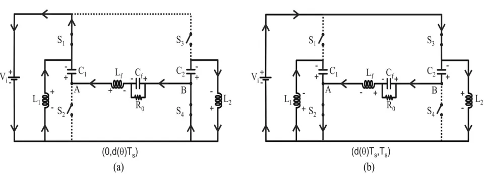
In order to gain an understanding of the system operation stages, the switches presented in Fig. 1 will be replaced by their bidirectional models. In order to illustrate the equivalent circuits of the system, two particular cases were chosen: the first refers to system operation with a duty cycle higher than 0.5, as shown in Fig.2, and the second the system operates with a duty cycle lower than 0.5, as depicted in Fig.3.
Fig.3: Equivalent circuits for duty cycle lower than 0.5: (a) stage related to the interval (0, d(θ)TS ); (b) stage related to the interval (d(θ)Ts, Ts ).
IV. THEORETICAL ANALYSIS
The functions involved in each operation stage and their respective equations are obtained for a fixed duty cycle considering one switching period and steady-state analysis, since transitory conditions and/or load variations were not considered. Table I shows the parameters and the mathematical functions for each variable of interest considering all operational stages and a duty cycle d(θ) higher than 0.5. These functions are sufficient to evaluate the instantaneous average values for the capacitor voltages and inductor currents.
A. Average Voltage in Capacitor C1
Equation (1) presents the inductor voltage across L1 for both operational stages. The expressions are indicated by the superscript numbers
<vL1 (t, )>Ts=1/TS{ vL1(1)(t, ).[d( ).TS]+ vL1(2)(t, ).[1-d( )].TS} (1)
Substituting the functions of vL1 (t, θ) shown in Table.3.1 into (1), it is possible to write (2), which represents the
average voltage applied to the capacitor C1
<vC1( )>Ts=Vi.[d( )/1-d( )] (2)
The duty cycle is given by (3), where M represents the modulation index
d( )=1/2[1+M sin( )] (3) B. Average Voltage across Capacitor C2
In (4) the voltage across inductor L2 , for the related operational stages, is represented
<vL2 (t, )>Ts=1/TS{ vL2(1)(t, ).[d( ).TS]+ vL2(2)(t, ).[1-d( )].TS} (4)
Substituting the functions related to the voltage across inductor L2 , detailed in Table. 3.1, in (4), it is possible to
find (5), which represents the average voltage across capacitor C2
<vC2( )>Ts=Vi.[1-d( )/ d( )] (5)
TABLE I: Parameters and Indicative Functions for the Stage of Operation
Parameters Stage 1 Stage 2
Time interval d( ).TS [1-d( )].TS
Inductor (L1) voltage Vi -<vC1( )>Ts
Inductor (L2) voltage -<vC2( )>Ts Vi
Capacitor (C1) current - <i0( )>Ts <iL1( )>Ts
Capacitor (C2) current -<iL2( )>Ts <i0( )>Ts
C. Average Current through Inductor L1
Based on the instantaneous average values, the current iC1 (t, θ) is presented as follows:
<iC1(t, )>Ts=1/TS{iC1(1)(t, ).[d( ).TS]+iC1(2)(t, ).[1d( )]. TS} (6)
On applying the operational stage functions, given in Table.3.1, it is possible to obtain (7), which represents the average current through inductor L1
<iL1( )>Ts=<i0( )>Ts.[d( )/ 1-d( )] (7)
D. Average Current through Inductor L2
A similar procedure applied to obtain the average current through L1 is performed for L2. In (8) the current iC2 (t, θ) is
shown, considering one switching period. Substituting the functions presented in Table.3.1 in (8), (9) is obtained. This expression represents the average current through inductor L2
<iC2 (t, )>Ts=1/TS{ iC2(1)(t, ).[d( ).TS]+ iC2(2)(t, ).[1-d( )].TS} (8)
<iL2( )>Ts= - <i0( )>Ts.[1-d( )/d( )] (9)
Fig. 10 shows the average currents through inductors L1 and L2 normalized with respect to the average output current. E. Static Gain, Current Ripple and Voltage Ripple
The static gain is determined by the relation between the average voltage <vAB (θ)>Tsand the input voltage Vi. In (10),
the equation for vAB(t, θ) is given for one switching period
<vAB (t, )>Ts=1/TS{ vAB(1)(t, ).[d( ).TS]+ vAB(2)(t, ).[1-d( )].TS} (10)
The functions that represent vAB(t, θ) in the related operational stages are indicated in Table.3.1. On substituting these
functions into (10), we obtain (11), which represents the static gain of the converter herein. In Fig. 11, the curve for the static gain in function of the duty cycle is shown
<vAB ( )>Ts/Vi = <q( )> Ts = [(2. d( ) – 1) / d( ).(1- d( )] (11)
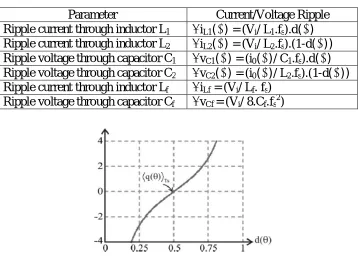
TABLE II: Ripple Currents through the Inductors and Ripple Voltages across the Capacitor
Parameter
Current/Voltage Ripple
Ripple current through inductor L
1∆
i
L1( )
= (V
i/ L
1.f
s).d
( )
Ripple current through inductor L
2∆
i
L2( )
= (V
i/ L
2.f
s).(1-d
( ))
Ripple voltage through capacitor C
1∆
v
C1( )
= (i
0( )
/ C
1.f
s).d
( )
Ripple voltage through capacitor C
2∆
v
C2( )
= (i
0( )
/ L
2.f
s).(1-d
( ))
Ripple current through inductor L
f∆
i
Lf= (V
i/ L
f. f
s)
Ripple voltage through capacitor C
f∆
v
Cf= (V
i/ 8.C
f.f
s2)
Fig.4: Static gain in function of the duty cycle.
F. Considerations Regarding Converter Operation
As a solution for this particularity, the desired voltage gain is used as the reference signal, which is applied at the input of the mathematical block, denominated by F (θ). The signal obtained at this function output is the operating duty cycle, and it enables the linearization of the relation between the desired static gain and that obtained at the converter output. The following equations show the steps applied to obtain the mathematical block that allows the representation of a sinusoidal output voltage with low distortion, independently of the desired voltage gain. The static gain of the new inverter topology is defined as follows:
d( ) = (<q( )>Ts -2) / 2.< q( )>Ts ± √(4+<q( )>2Ts) / 2. <q( )>Ts (12)
Manipulating (12) the duty cycle, as a function of the static gain, is presented as follows:
( ) = (<q( )>Ts -2) / 2. < q( )>Ts + √(4+<q( )>2Ts) / 2. <q( )>T (13)
Voltage (V)
Fig.5: Simulation results: (a) output voltage without the linearization function ;(b) output voltage with linearization function.
In order to demonstrate the efficiency of the linearization function, the simulation results for the converter output voltage without and with F(θ) are presented in Fig. 12, for a static gain of four. It was verified that the use of the linearization function is sufficient to establish a linear relation between the real and the reference static gain, as shown in Fig. 12.
V. PI CONTROLLER
In general PI controller has the ability to reject disturbances and can stabilize the process. A PIC provides proficient output voltage regulation and reduced steady state error for the converter. The dc output voltage is sensed and compared with reference output voltage, which gives the error signal. This error signal is processed by the PIC to keep the output voltage constant and reduce the steady state error.
VI. FUZZY LOGIC SYSTEM
Fig.6: Block Diagram of FLC
The fuzzifier has the effect of transforming crisp measured data into suitable linguistic values (i.e. fuzzy sets).The fuzzy rule base stores the empirical knowledge of the operation of the process of the domain experts. The inference engine is the kernel of a FLC, and it has the capability of simulating human decision making by performing approximate reasoning to achieve a desired control strategy. The defuzzifieris utilized to yield a nonfuzzy decision or control action from an inferred fuzzy control action by the inference engine.
VII. SIMULATION RESULTS
A prototype of the proposed converter was simulated through MATLAB. The converter was tested with Vin =96V DC,
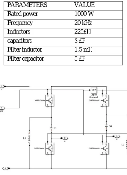
Vo = 110V AC, further design parameters are given in Table I and simulation parameters are given in table III. TABLE III: Simulation Parameters
Fig.7: Simulation Diagram of inverter
PARAMETERS VALUE
Rated power 1000 W
Frequency 20 kHz
Inductors 225μH
capacitors 1 μF
Fig.8: Simulation Diagram of converter with PI controller
Fig.7 shows the simulation diagram of inverter. It is the subsystem of the fig. 8 which shows the simulation diagram of converter with PI controller.Fig.9 shows output waveform of simulation diagram of converter with PI controller. And it’s efficiency shows in fig.10.
Time in (seconds)
Fig.9: Output Waveform
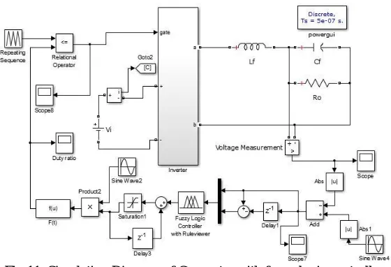
Fig.11: Simulation Diagram of Converter with fuzzy logic controller
Fig. 11 shows the simulation diagram of converter with fuzzy logic controller whose subsystem shows in fig.7. The output waveform of simulation diagram of converter with fuzzy logic controller shows in Fig.12. And its efficiency shows in fig.13.
Time in (seconds)
Fig.12: Output Waveform
VIII. CONCLUSION
A new topology for dc–ac converters is introduced whose main feature is its capacity to provide an instantaneous output voltage higher or lower than the input voltage without an intermediate power stage or transformer. It is suitable for wide input range and it is basically a buck-boost inverter. The new inverter having a simple topology and there are only a few components in overall system. The functions involved in each operation stage and their respective equations are studied for a fixed duty cycle considering one switching period. Equations for the ripple currents and voltages were found. Here the static gain can be linearised using linearization function. So that the gain directly proportional to the duty cycle.
Closed loop performance of step up/step down DC-AC converter with fuzzy logic controller and PI controller have been studied and verified through simulation. Simulation results show that the proposed strategy with fuzzy logic controller works well and reduces the peak overshoot and settling time as compared to the inverter with PI controller.
REFERENCES
[1] R. O. Caceres and I. Barbi, “A boost DC–AC converter: analysis, design, and experimentation,” IEEE Trans. Power Electron., vol. 14, no. 1,pp. 134–141, Jan. 1999.
[2] N.Vazquez, J.Villegas-Saucillo, C.Hernandez, E. Rodriguez, and J. Arau, “Two-stage uninterruptible power supply with high power factor,”
IEEE Trans. Ind. Electron., vol. 55, no. 8, pp. 2954–2962, Aug. 2008.
[3] S. B. Kjaer, J. K. Pedersen, and F. Blaabjerg, “A review of single-phase grid-connected inverters for photovoltaic modules,” IEEE Trans. Ind.Appl., vol. 41, no. 5, pp. 1292–1306, Sep./Oct. 2005.
[4] S.Miaosen and F. Z. Peng, “Operation modes and characteristics of the Z source inverter with small inductance,” in Proc. 40th IAS Annu. Meeting.Conf. Rec. Ind. Appl. Conf., vol. 2, pp. 1253–1260,2005.
[5] X. Yaosuo, C. Liuchen, K. Sren Baekhj, J. Bordonau, and T.Shimizu,“Topologies of single-phase inverters for small distributed power generators:An overview,” IEEE Trans. Power Electron., vol. 19, pp. 1305–1314, 2004.
[6] Ritu Shakya, Kritika Rajanwal, Sanskriti Patel and Smita Dinkar, “Design and Simulation of PD, PID and Fuzzy Logic Controller for Industrial Application,” International Journal of Information and Computation Technology, ISSN 0974-2239 ,vol 4, no. 4, pp. 363-368, 2014.
[7] Wing-Chi So,Chi K.Tse,Yim-Shu Lee“Development of fuzzy logic controller for DC/DC converters: design, Computer simulation,and Experimental Evaluation,” IEEE Trans.power electron.vol.11,no.1,Jan. 1996.
[8] S.Sathya, C.karthikeyan,“Fuzzy Logic Based Z-Source Inverter for Hybrid Energy Resources,” International Journal of Engineering Science and Innovative Technology (IJESIT) vol. 2, Issue 4, July 2013.
[9] R.Anand,I.Gnanambal, N.Poornema,“Implementation of fuzzy logic controller for buck-boost converter combining KY and synchronous buck converter for battery operated portable devices,” Journal of Theoretical and Applied Information Technology, Vol. 67 No.1.Sep.2014. [10] Gaurav, Amrit Kaur,“Comparison between Conventional PID and Fuzzy Logic Controller for Liquid Flow Control: Performance Evaluation of