Implementation of Double Precision Floating
Point Multiplier on FPGA
A.Keerthi1, K.V.Koteswararao2
PG Student [VLSI], Dept. of ECE, Sree Vidyanikethan Engineering College, Tirupati, India1
Assistant professor, Dept. of ECE, Sree Vidyanikethan Engineering College, Tirupati, India2
ABSTRACT: Multiplication is one of the common arithmetic operations in Digital Signal Processing(DSP) computations. The proposed design is an implementation of an IEEE-754 Double Precision Floating Point Multiplier, which is better when compared to a single precision multiplier[1] because of its wider dynamic ranges and accuracy. A Double Precision Multiplier is designed using Xilinx 12.4 ISE tool and the design verification was done on Xilinx Vertex-4 ML403 platform which handles overflow, underflow cases and Truncation mode. A Comprehensive simulation and analysis of multiplier output is done using Xilinx ISim simulator and a test bench is written to generate an input stimulus.
KEYWORDS: Double precision, Floating point, Multiplier, FPGA, Digital Signal Processing, IEEE-754.
I.INTRODUCTION
Mostly, Floating Point arithmetics[2] are having wider dynamic range and accuracy because of this feature they are used in application specific systems like DSP[3]. Floating Point arithmetics involve different operations[4] such as addition, subtraction, multiplication, division, etc., of which multiplication is one of the core operation in many signal processing computations. A large number of Floating Point multiplications are carried out in applications such as scientific calculation and computer graphics (CG). CG, in particular, requires enormous amount of FP multiplications to obtain high quality images required for multimedia systems. It is also of key importance to many modern applications such as 3D graphics accelerators, Digital Signal Processors (DSPs), High Performance Computing etc.
II.RELATED WORK
Most of the researchers implemented Floating Point arithmetics in their own way. The concept of IEEE single precision floating Point Multiplier[1] was implemented efficiently by Mohamed Al-Ashrafy , Ashraf Salem and Wagdy Anis in “ An efficient implementation of floating point multiplier,” the number of slices used here are 604 and the frequency is 301.114MHz, with a latency of 3 cycles is obtained. Addanki Puma Ramesh, A. V. N. Tilak, A.M.Prasad defined about double precision floating point multiplier in [7] “An FPGA Based High Speed IEEE-754 Double Precision Floating Point Multiplier Using Verilog”. The area occupies 648 slices and the operating frequency is 414.714MFLOPS.
III.FLOATING POINT FORMAT
The IEEE-754 standard[5] format has two different formats the binary format and the decimal format. A Double Precision Floating Point Multiplier in IEEE-754 binary format is seen in the fig 1. The Double Precision Floating Point Multiplier consists of 64 bits in which the sign bit is represented by 1 bit the exponent bit is represented by 11bits, and the mantissa bit is of 52 bits.
range from −1023 to +1024. The double precision format offers a range from 2-1023 to 2+1023, which is equivalent to 10-308 to 10+308.
Fig 1: IEEE-754 Double Precision Floating Point Format
IV. FLOATING POINT MULTIPLIER ALGORITHM
The normalized floating point numbers have the form of Z= (-1)S * 2 (E - Bias) * (1.M). The following algorithm is used to multiply two floating point numbers.
1. Significand multiplication; i.e. (1.M1*1.M2). 2. Placing the decimal point in the result. 3. Exponent’s addition; i.e. (E1 + E2 - Bias). 4. Getting the sign; i.e. s1 xor s2.
5. Normalizing the result; i.e. obtaining 1 at the MSB of the results’ significand. 6. Rounding implementation.
7. Verifying for underflow/overflow occurrence.
V.IMPLEMENTATIONOF FLOATING POINT MULIPLIER
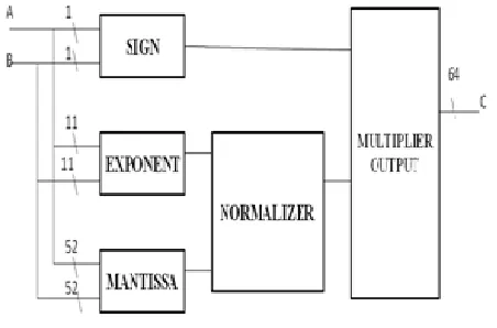
Fig.2 Floating Point Multiplier.
Consider two operands A and B. Then the floating point multiplier in fig 2 consists of SIGN CALCULATION: If the number is a positive number then the sign bit is ‘0’ otherwise ‘1’.Adding the two sign bits gives the resultant sign value which is the XOR operation of two numbers.
2.The second stage of carry save multiplier is having (Significand digit - 2)adders, which are full adders 3.The third stage is an array of ripple carry adder i.e., a half adder and a full adder.
NORMALISER: The result of the significand multiplication (intermediate product) must be normalized to have a leading ‘1’ just to the left of the decimal point (i.e. in the bit 46 in the intermediate product). Since the inputs are normalized numbers then the intermediate product has the leading one at bit 46 or 47
1- If the leading one is at bit 46 (i.e. to the left of the decimal point) then the intermediate product is already a normalized number and no shift is needed.
2- If the leading one is at bit 47 then the intermediate product is shifted to the right and the exponent is incremented by 1.
MULTIPLIER OUTPUT: The resultant output is obtained is then checked for Overflow and underflow.
OVERFLOW AND UNDERFLOW: Since the exponent value is 11 bits the range of a Double Precision Floating Point
Multiplier is -2n-1 to +2n-1 i.e., is -2047 to +2047. If the range is greater then +2047 than Overflow occurs or if the range is less than -2047 then Underflow occurs.
VI. COREGENERATOR
In order to convert a fixed number to floating point number a fixed to float floating point core generator is used and fed to a double precision floating point multiplier. In Fig 3 A, B represents two fixed operands which are converted to floating point number.
Fig.3 Double Presicion Floating Point Multiplier with Fixed to Float core generator and a Counter
VII. TESTING
After the implementation of a code testing is to be done in order to verify whether the coding is correct or incorrect. It is done in two ways.
1.It is tested for a dynamic range of values independently.
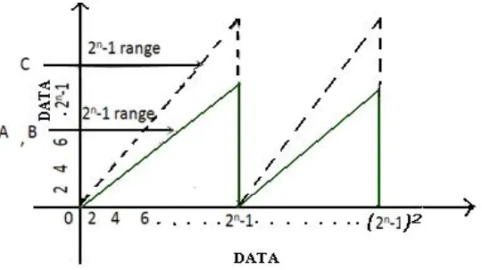
2. A counter is used as a part of testing for wider dynamic ranges. If the counter is n bit then the output of the counter has 2n ranges(i.e., 0 to 2n-1). The obtained range of values is given to the input of fixed to float Double precision floating Point Multiplier as shown in fig.3.As a Double Precision Floating Point Multiplier is 64 bit wide the output obtained is of 264 bit.
VIII. RESULT AND DISCUSSION
Fig.4 Simulation Diagram of Double Presicion Floating Point Multiplier
In fig 5 the graph shows the Data Vs Data output which is obtained in Chipscope Analyzer. The waveform is a ramp signal for different dynamic ranges. Table I shows the logic utilisation of a double precision floating point multiplier.
Fig. 5 Chipscope output for Data vs Data
Table I
Design Summary of Double Precision Floating Point Multiplier.
Logic Utilization Used
Number of Slices occupied 4437
Number of bonded IOBs 192
IX.CONCLUSION
X.ACKNOWLEDGEMENT
A. Keerthi would like to thank K.V.Koteswararao, Assistant professor ECE Department who had been guiding throughout the project and supporting me in giving technical ideas about the paper and motivating me to complete the work efficiently and successfully.
REFERENCES
[1] Mohamed AI-Ashraf', Ashraf Salem, Wagdy Anis., "An Efficient Implementation of Floating Point Multiplier ", Saudi International Electronics, Communications and Photonics Conference (SIECPC), pp. 1-5, 2011.
[2] A. Jaenicke and W. Luk, "Parameterized Floating-Point Arithmetic on FPGAs", Proc. of IEEE lCASSP, vol. 2, pp. 897-900,2001.
[3] J.A. Eldon and C. Robertson, “A Floating Point Format for Signal Processing,” Proceedings IEEE International Conference on Acoustics, Speech, and Signal Processing, pp, 717-720,1982.
[4] B. Lee and N. Burgess, “Parameterisable Floating-point Operations on FPGA,” Conference Record of the Thirty-Sixth Asilomar Conference on Signals, Systems, and Computers, 2002.
[5] IEEE 754-2008, IEEE Standard for Floating-Point Arithmetic, 2008.
[6] B. Fagin and C. Renard, “Field Programmable Gate Arrays and Floating Point Arithmetic,’’ IEEE Transactions on VU], Vol. 2, No. 3, pp. 365-367, September 1994.
[7] Addanki Puma Ramesh, A. V. N. Tilak, A.M.Prasad., “An FPGA Based High Speed IEEE-754 Double Precision Floating Point Multiplier Using Verilog” International Conference on Emerging trends in VLSI, Embedded System, Nano Electronics and Telecommunication System (ICEVENT),pp. 1-5,2013
BIOGRAPHY
A.Keerthi completed her B.Tech in Electrical and Electronics Engineering from Kandula Lakshumma memorial College of Engineering for Women, Kadapa, Andhra Pradesh, India in 2012. She is now pursuing her Master of Technology (M.Tech) in VLSI at Sree Vidyanikethan Engineering College, Tirupati, Andhra Pradesh, India. Her interest includes Digital Design, Low Power VLSI.