Available Online at www.ijcsmc.com
International Journal of Computer Science and Mobile Computing
A Monthly Journal of Computer Science and Information Technology
ISSN 2320–088X
IJCSMC, Vol. 4, Issue. 3, March 2015, pg.371 – 382
RESEARCH ARTICLE
A Review on Existing Clock Gating
Dushyant Kumar Soni
1, Ashish Hiradhar
2Department of Electronics & Communication
Dr. C V Raman University Bilaspur (C.G.)
[email protected]; [email protected]
Abstract— In present era every multimedia and DSP based devices will work on some certain clock and as we know, clock signal having great source of power consumption and this is a critical problem in every synchronous circuit. Clock gating is an effective way of reducing the dynamic power dissipation in digital circuits. In a typical synchronous circuit such as the general purpose microprocessor, only a portion of the circuit is active at any given time. Hence, by shutting down the idle portion of the circuit, the unnecessary power consumption can be prevented. One of the ways to achieve this is by masking the clock that goes to the idle portion of the circuit. In This project I will present a review on existing clock gating approaches and also make a comparative analysis of those clock gating technique on some synchronous digital design like ALU (Arithmetic logical unit) and FIFO(first in first out) etc. Also I will propose a new clock gating technique which will provide more immunity to the existing problem in available technique.
Keywords— clock gating, synchronous circuit, VLSI, EDA, DSP
I. INTRODUCTION
In recent years, the demand for power-sensitive designs has grown significantly. This tremendous demand has mainly been due to the fast growth of battery-operated portable applications such as notebook and laptop computers [16], personal digital assistants, cellular phones, and other portable communication devices. Semiconductor devices are aggressively scaled each technology generation to achieve high-performance and high integration density. Due to increased density of transistors in a die and higher frequencies of operation, the power consumption in a die is increasing every technology generation. Supply voltage is scaled to maintain the power consumption within limit. However, scaling of supply voltage is limited by the high-performance requirement. Hence, the scaling of supply voltage only may not be sufficient to maintain the power density within limit, which is required for power-sensitive applications. Circuit technique and system-level techniques are also required along with supply voltage scaling to achieve low-power designs.
systems increases the complexity of the clock network and hence increases the clock power even if the clock frequency may not scale anymore. Hence, the major fraction of the total power consumption in highly synchronous systems, such as microprocessors, is due to the clock network. In the Xeon Dual-core processor, a significant portion of the total chip power is due to the clock distribution network [2]. Thus, innovative clocking techniques for decreasing the power consumption of the clock networks are required for future high performance and low power designs.
Electronic design automation (EDA or ECAD) is a software tools for designing electronic systems such as printed circuit boards and integrated circuits. The tools work together in a flow and analysis required design & its outcome that connects the chip designers to work in all abstraction levels of semiconductor chip [3]. The EDA is formally known as Engineering Design Automation which has been become a part of necessary part of the design automation tools. To reduce the design time for a system, Many EDA tools are introduced with lot of feature involve, in the market. As most important chip design parameter are Area, Power and Performance. Area is calculated at most in terms of gate count or transistor count or the final chip area including transistor and interconnects with routing conductor. The optimization is done with the routing/placement/positioning algorithm to get the optimized results. Next is the Performance of the design it is the logic levels, gain, working frequency, temperature analysis, reliability, etc. These two can be separately deal in the each & every abstraction level of design to make it optimized. But power is the parameter which is the dependant on many factors like area, routing cost, logic implementation and many more. Since Power is divided into two types i.e. static power (power dissipated when circuit is in OFF state), Dynamic power (power dissipated when circuit is switching from one state to another or ON state).So, power management has become a serious problem to overcome. This report deals with Power management aspects used by the EDA tools and its optimization problem, which integrates with the process to device development and includes chip architects, circuit and logic designers along with EDA developer to have an automated Environment promising the optimization of power management techniques.
A spectrum of circuit techniques including transistor sizing, clock gating, multiple and dynamic supply voltage are there to reduce the dynamic power. Clock gating is one of the popular techniques for reducing clock power [4]. The existing clock gating solutions are based on masking the local clock signal using masking logic gates (NAND/NOR) [4].
II. REVIEW ON EXISTING CLOCK GATING
There are following different techniques for clock gating as discussed below:
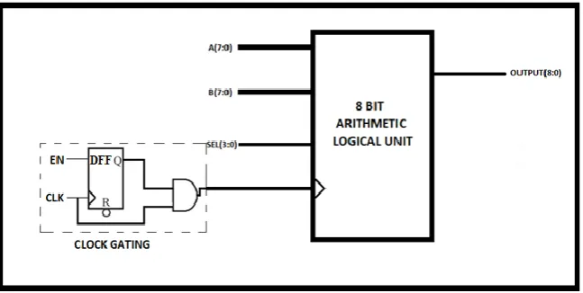
A. AND GATES
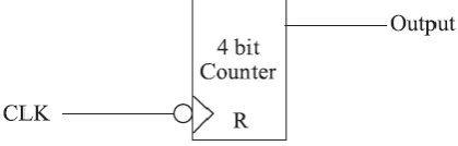
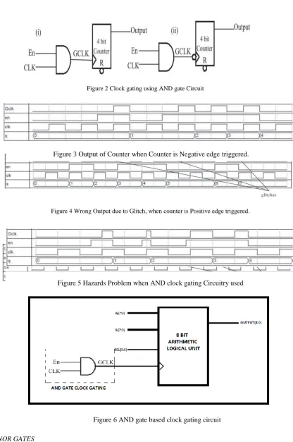
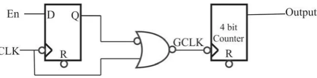
Initially many authors suggested using AND gate for Clock gating because of its simple logic [6][9][13]. In sequential circuit one two-input AND gate is inserted in logic for clock gating. One input to AND gate is clock and while the second input is a signal used to control the output (means it will control the sequential circuit's clock). for experimental purpose we are taking a simple counter shown in Figure 1 as a sequential circuit application. Figure 2 shows the clock gating technique for the counter by inserting one AND Gate. Figure 3 shows the output of counter when counter is negative edge triggered and enable ('en') changes from clock cycle starting from negative edge to the next negative edge, in this case output of the counter changes after one clock cycle of being en='1'. From Figure 4 we have observed that when counter is positive edge triggered and enable is changing starting from positive edge to the next positive edge, counter increments one extra time, due to tiny "Glitch", when it goes down due to more falling time of the enable, and the output in this case is wrong.
In Figure 5 we have shown a major problem of Hazards when any hazard at the enable could be pass on to the Gclk when clk='1' this situation is particularly very dangerous and could jeopardize the correct functioning of the entire system [11] In the below circuit the AND gated clock gating is applied to an 8bit ALU. The GCLK is the signal is the gated clock signal which controls the clock signal of ALU. The en signal is used to enable and disable the clock to reduce the power consumption of ALU . The GCLK signal is passed only when both en and clk signal are high, thus out of two edges of clock the ALU is active for only one cycle of clock.
B. NOR GATES
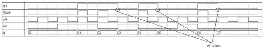
Title NOR gate is a very suitable technique for clock gating where we need actions to be performed on Positive Edge of the Global clock [11][13].For analysis using NOR gate, the circuit connection is shown in Figure 7; in this figure we can observe that Counter will work when enable turn "ON".Figure 8 shows the waveform for incorrect output of the Counter when enable changes to '1' at negative edge of the clock. Incorrect output is due to the small glitch when enable turns low at negative edge of the clock, counter increments one more clock. Figure 9 shows output of Counter when enable changes from positive edge to next positive edge but counter is
Figure 2 Clock gating using AND gate Circuit
Figure 3 Output of Counter when Counter is Negative edge triggered.
Figure 4 Wrong Output due to Glitch, when counter is Positive edge triggered.
Figure 5 Hazards Problem when AND clock gating Circuitry used
negative edge triggered. Figure 10 shows correct output of the counter with positive edge triggered because enable is changing from positive edge of the clock to the next positive edge of the clock. In the figure 11 we have shown a major problem of Hazards. When any hazard at the enable could be pass on to the Gclk when clk='0' this situation is particularly very dangerous and could jeopardize the correct functioning of the entire system [11].
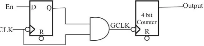
C. LATCH BASED AND GATE CLOCK GATING
Latch Based AND Gated Clock circuit is shown in Figure 4(A). The enable signal 'En' is applied through a latch to overcome the previous problems of incorrect output in place of directly connected to AND gate. The Latch is
Figure 1 Clock gating of negative edge counter using negative Latch Based AND gate Circuit
Figure 2 Normal output of Negative edge Counter when negative Latch based AND Gated Clock is used.
Figure 3 Output of negative edge counter when there are some random Hazards at En
Figure 4 Clock gating of positive edge counter using positive Latch Based AND gate Circuit.
needed for correct behaviour, because En might have Hazards that must not propagate through AND gate when Global clock is '1' [11][13][15]. However, the delay of the logic for the computation of En may on the critical path of the circuit will increase and its effect must be taken into account during time verification [11][14][15][13].It is clear from Figure 4(B) that counter will take one extra clock cycle delay to change its state and after that it will work normally until, En is de-asserted and this time also it will take one clock cycle extra to stop changing its state. Figure 4(C) verifies that unwanted outputs due to Hazards at the En are avoided. Figure 4(E) waveform show that when controlling latch is positive and counter is also positive edge triggered then output of the counter is incorrect because it increments once even when enable is turned down due to a tiny glitch.
D. LATCH BASED NOR GATE CLOCK GATING
Latch based NOR Gated Clock scheme is shown in Figure 17. Here enable signal is applied through latch in place of direct connection to NOR gate [11][13][18].We can observe from Figure that counter will take one extra clock cycle delay to change its state and after that it will work normally until En is de-asserted and this
Figure 12 Clock gating of negative edge counter using negative Latch Based AND gate Circuit
Figure 13 Normal output of Negative edge Counter when negative Latch based AND Gated Clock is used.
Figure 14 Output of negative edge counter when there are some random Hazards at En
Figure 15 Clock gating of positive edge counter using positive Latch Based AND gate Circuit.
time also it will take one clock cycle extra to stop changing its state. In Figure 19 we have verified that unwanted outputs due to Glitches at the En are avoided. In Figure 21 waveform the case when controlling Latch is negative and Counter is also negative edge triggered is shown. The output of the counter is incorrect because it increments once even when enable is turned down due to a tiny glitch due to the fall time delay of enable.
Figure 17 Clock gating of negative edge counter using positive Latch Based NOR gate Circuit
Figure 18 Normal output of negative edge Counter when positive Latch based OR Gated Clock is used.
Figure 19 Output of negative edge counter when there are some random Hazards at En
E. MUX BASED CLOCK GATING
In mux based clock gating [13][11] we use multiplexer to close and open a feedback loop around a basic D-type flip-flop under control of the enable signal as shown in Figure . As the resulting circuit is simple, robust, and compliant with the rules of synchronous design this is a safe and often also a reasonable choice. On the negative side, this approach takes one fairly expensive multiplexer per bit and consumes more power. This is because any toggling of the clock input of a disabled flip-flop amounts to wasting of energy in discharging and recharging the associated node capacitances for nothing. The capacitance of the CLK input is not the only contribution as any clock edge causes further nodes to toggle within the flip-flop itself [11]. In Figure waveform of Negative Edge triggered Counter is shown and in Positive edge triggered. We can observe from these waveforms that when En turns ON then at each Negative and Positive Edge of the clock respectively counter increments and when En goes Low counter holds its state.
Figure 6 Output of counter when latch is negative and Counter also negative edge triggered
Figure 22 Generation of Gated Clock When Negative Latch is used
F. FLIP FLOP BASED CLOCK GATING
In FF based clock gating, FF is used as control element. When the negative edge of clock arrives, change of Enable will be reflected on FF output. If output of FF is high, clock is applied on sequential circuit. The sleep period is longer in FF based clock gating compared to Latch based clock gating. It means there is a greater chance to miss the change that happens on Enable signal.
G. POSITIVE LEVEL-SENSITIVE LATCH BASED CLOCK GATING
Fig. 26 shows the schematic diagram of a clock gating applied to a D-type flip-flop. This circuit consists of D latch to store the data. An XOR logic gate is used to compare incoming data with the stored data, and an AND gate to block the clock signal when the input and the stored data are the same and the change is not necessary.[20] This circuit is work as when the data come it compare with store data. If this data is same as the store data, the ckg=0 and the circuit will be in the standby mode. If the data is different from the store data the latch will be transparent when ckg=1.
Figure 24 Output of positive edge Counter with gated clock for circuit
H. T FLIP FLOP BASED CLOCK GATING
In the clock gating using the latch, the data line connected to the D flip flop(FF), when a change is required and in the case when change is not required, the connection is not needed and its existence may increases the data line loading. To remove this problem we use the Clock gating using T FF. T-type in Fig27. makes it possible to disconnect data input line from the flip-flop and connect it only to the clock-gating circuitry. In this case when the data and stored are different T FF will toggle and change in output will occur [21]
I. DOUBLE GATED FLIP-FLOPBASED CLOCK GATING
A general implementation of Double Gating is presented in figure.16 The technique uses two gated latches in a master slave configuration. The first gated latch is positive sensitive and the second one is negative level-sensitive. This technique yields a reliable gated flip-flop that can be used with any clock duty-cycle and is suitable for standard cell design. In the double Gated when clock is high the master is active and on negative clock slave will transparent.[19][20]
Figure 26 Positive level sensitive latch based clock gating circuit
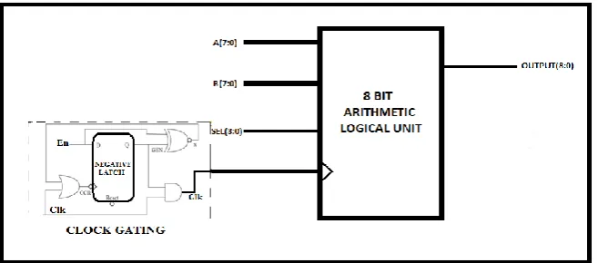
J. GATED CLOCK USING NEGATIVE LATCH BASED CLOCK GATING
The working of the figure can be understood as when En=1 at that time GEN=0, then XNOR will produce a 0 output. This goes to the first clock generation logic that generate clock for controlling device. The global clock is connected to OR gate, that logic will generate the clock pulse that will drive the controlling latch. Form this Gated clock one can save more power because device is on when only the input En is changing.[19][20]
III. PROBLEM IDENTIFICATION
In previous all clock gating approaches are facing with the problem of size means those approach which are require less size there is some other issue of glitches and those approaches which having large size so there is no any glitches problem but those structure are increase static problem. In all previous approach only few approaches will reduce the clock power but still some are facing the problem of clock power. In some previous architecture there is need of extra input and output pins as we know for VLSI chip increase in input and output pins will increase the cost of the whole process.
IV. CONCLUSIONS
In first two techniques, AND and NOR based clock gating, we have output correctness problem due to Glitches and Hazards. Where in latch based AND and NOR techniques Hazards problem is removed. However Glitches problem still exists in them. In fifth techniques we does not have these problem but still we cannot consider it very good power saving technique. Mux based clock gating takes one fairly expensive multiplexer per bit and consumes more power. In FF based clock gating the sleep period is longer compared to Latch based clock gating. It means there is a greater chance to miss the change that happens on Enable signal. In previous all clock gating approaches are facing with the problem of size means those approach which are require less size there is some other issue of glitches and those approaches which having large size so there is no any glitches problem but those structure are increase static problem. In all previous approach only few approach will reduce the clock
Figure 28. Double gated FF based clock gating circuit
power but still some are facing the problem of clock power. In some previous architecture there is need of extra input and output pins as we know for VLSI chip increase in input and output pins will increase the cost of the whole process.
REFERENCES
[1] Bipul C. Paul, Amit Agarwal, Kaushik Roy, ―Low-power design techniques for scaled technologies‖,
INTEGRATION, the VLSI journal, science direct 39(2006).
[2] L. Hai, S. Bhunia, Y. Chen, K. Roy, T.N. Vijay Kumar, ― DCG : deterministic clock gating for low-power microprocessor design ‖, IEEE Trans. VLSI Syst. 12 (2004), pp.245-254.
[3] Hai Li, Swarup Bhunia, Yiran Chen, T. N. Vijaykumar, and Kaushik Roy, ―Deterministic Clock Gating for
Microprocessor Power Reduction‖,1285 EE Building, ECE Department, Purdue University
[4] N. Raghavan, V. Akella, S. Bakshi, ―Automatic insertion of gated clocks at register transfer level‖, in:
International Conference on VLSI Design, 1999, pp. 48 – 54.
[5] Kawa, J., "Low Power and Power Management for CMOS—An EDA Perspective," Electron Devices, IEEE Transactions on , vol.55, no.1, pp.186,196, Jan. 2008
[6] Borkar, S., "Design challenges of technology scaling," Micro, IEEE, vol.19, no.4, pp.23, 29, Jul-Aug 1999.
[7] Strollo, A. G M; Napoli, E.; De Caro, D., "New clock-gating techniques for low-power flip-flops," Low Power Electronics and Design, 2000. ISLPED '00. Proceedings of the 2000 International Symposium on, vol., no., pp.114, 119, 2000.
[8] Alidash, H.K.; Sayedi, S.M., "Activity aware clock gated storage element design," Electrical Engineering (ICEE), 2011 19th Iranian Conference on, vol., no., pp.1, 1, 17-19 May 2011.
[9] Yan Zhang; Roivainen, J.; Mammela, A., "Clock-Gating in FPGAs: A Novel and Comparative Evaluation," Digital System Design: Architectures, Methods and Tools, 2006. DSD 2006. 9th EUROMICRO Conference on , vol., no., pp.`584,590, 0-0 0
[10] Shaker, M.O.; Bayoumi, M.A., "A clock gated flip-flop for low power applications in 90 nm CMOS," Circuits and Systems (ISCAS), 2011 IEEE International Symposium on, vol., no., pp.558, 562, 15-18 May 2011.
[11] Sulaiman, D.R., "Using clock gating technique for energy reduction in portable computers," Computer and Communication Engineering, 2008. ICCCE 2008. International Conference on, vol., no., pp.839, 842, 13-15 May 2008.
[12] Teng Siong Kiong; Soin, N., "Low power clock gates optimization for clock tree distribution," Quality Electronic Design (ISQED), 2010 11th International Symposium on, vol., no., pp.488, 492, 22-24 March 2010.
[13] Kathuria, J. ; Ayoubkhan, M. ; Noor, A. ; ―A Review of Clock Gating Techniques‖, MIT International Journal of Electronics and Communication Engineering, August 2011, vol.1 no.2 , pp 106-114.
[14] Shinde, J.; Salankar, S.S., "Clock gating — A power optimizing technique for VLSI circuits," India Conference (INDICON), 2011 Annual IEEE , vol., no., pp.1,4, 16-18 Dec. 2011.
[15] Tomar, B.P.S.; Chaurasia, V.; Yadav, J.; Pandey, B., "Power Reduction of ITC'99-b01 Benchmark Circuit Using Clock Gating Technique," Computational Intelligence and Communication Networks (CICN), 2013 5th International Conference on , vol., no., pp.423,427, 27-29 Sept. 2013
[16] Sterpone, L.; Carro, L.; Matos, D.; Wong, S.; Fakhar, F., "A new reconfigurable clock-gating technique for low power SRAM-based FPGAs," Design, Automation & Test in Europe Conference & Exhibition (DATE), 2011 , vol., no., pp.1,6, 14-18 March 2011
[17] He m nek, A.; Kune , M.; Tich , M., Reducing Power Consumption of an Embedded DSP Platform
through the Clock-Gating Technique," Field Programmable Logic and Applications (FPL), 2010 International Conference on , vol., no., pp.336,339, Aug. 31 2010-Sept. 2 2010
[18] Wimer, S.; Koren, I., "The Optimal Fan-Out of Clock Network for Power Minimization by Adaptive Gating," Very Large Scale Integration (VLSI) Systems, IEEE Transactions on , vol.20, no.10, pp.1772,1780, Oct. 2012
[19] Yunlong Zhang; Qiang Tong; Li Li; Wei Wang; Ken Choi; JongEun Jang; Hyobin Jung; Si-Young Ahn, "Automatic Register Transfer level CAD tool design for advanced clock gating and low power schemes," SoC Design Conference (ISOCC), 2012 International , vol., no., pp.21,24, 4-7 Nov. 2012
[21] Pandey, B.; Yadav, J.; Pattanaik, M.; Rajoria, N., "Clock gating based energy efficient ALU design and implementation on FPGA," Energy Efficient Technologies for Sustainability (ICEETS), 2013 International Conference on , vol., no., pp.93,97, 10-12 April 2013