High Speed Low Power Self Timed CAM
Application Based On Reordered Overlapped
Search Method
P.Uma Devi1, Mr.P.Sukumar2
1
PG Scholar,2ASP of ECE, 1,2Nandha Engineering College, Erode
Abstract—This paper introduces a reordered overlapped search mechanism for high-throughput low-energy content-addressable memories (CAMs). Most mismatches can be found by searching a few bits of a search word. To lower power dissipation, a word circuit is often divided into two sections that are sequentially searched or even pipelined. Because of this process, most of match lines in the second section are unused. Since searching the last few bits is very fast compared to searching the rest of the bits, we propose to increase throughput by asynchronously initiating second-stage searches on the unused match lines as soon as a first-stage search is complete. This allows the circuits to be in the required phase for their own local operation: evaluate or precharge, instead of having to synchronize their phase to the rest of the word circuits, which greatly reduces the cycle time. The proposed asynchronous CAM operates faster than a synchronous CAM with smaller energy dissipation. An internet protocol (IP) filter is used to unblock particular applications which determine the next hop for a packet by
finding the longest prefix match. This lookup often occurs in content addressable memory (CAM), which allows bit masking of the IP address.
Index Terms—CAM, Asynchronous circuits, associative memory, NAND-type CAM, IP filter
I. INTRODUCTION
Content-addressable memory (CAM) is a special type of computer memory used in certain very-high-speed searching applications. It compares input search data against a table of stored data, and returns the address of matching data. CAMs are used for many applications, such as Data Compression, Network Switch, IP Filters, IP Address Resolution, ATM Switch, Cache Tags, Cache for Large External CAM, Cache Reference Design CAMs often contain a few hundred to 32 K entries for net-work routers, where each entry or word circuit contains several dozens of CAM cells. Each input-search bit is compared with its CAM-cell bit and the comparison result determines whether a pass transistor in the CAM cell attached to the match line (ML) of a word circuit is in on or off states
CAM cells are used w i t h N A N D t yp e c e l l s i n t h e e xi s t i n g s y s t e m . A NAND-type word circuit operates at medium speed because pass transistors are connected seri-ally between a ML to a ground line. Because very few matched word circuits discharge their ML capacitances, a NAND-type word circuit reduces the power dissipation of MLs type word circuit. To improve the throughput of the NAND-type word circuit, some techniques at the circuit level [11], [12]. In this paper, we introduce a reordered overlapped search mechanism for a high-throughput low energy CAM version of this mechanism in [17] and this work is the extension. It includes two new approaches: a reordered word-overlapped search (RWOS) at the scheduling level and phase-word-overlapped processing (POP) at the circuit level. In a CAM, most mismatches can be found by searching a few bits of a search word. In the proposed CAM, An IP filter is a security feature that prohibits unauthorized users from accessing LAN resources. It can also restrict IP traffic over a wide-area network (WAN) link. With an IP filter, LAN users can be restricted to specific applications on the Internet (such as e-mail). CAM works as a filter to block all access except for packets that have permission. The addresses that have permission are stored in CAM; when an address is sent to memory, CAM reports whether it contains the address. If the address resides within CAM, it has permission for a particular activity. When multiple permissions are required, a combination of CAM and RAM enables this operation. A sample application that regulates access to e-mail, the web, file transfer protocol (FTP), and telnet. This application uses a 4-bit RAM block; each bit of RAM refers to one permission or access.
In the proposed RWOS scheme, an input word is assigned to word circuits at a rate based on the short delay of the
468
search is only initiated once the current search has completed in both segments.
[image:3.612.213.421.97.208.2]
Fig.1 Block diagram of Content Addressable Memory
II. REVIEW OF CONTENT ADDRESSABLE MEMORY
Fig. 1 shows a block diagram of a CAM. A search word is broadcast onto search lines (SLs) to the table of stored words whose sizes are n bits. The number of bits n in a CAM word usually ranges from 36 to 144 bits. A typical CAM employs a table size ranging between a few hundred entries to 32 K entries. Each word block has a match line (ML) that indicates whether search and stored words are the same or different. The outputs of the word blocks are fed to an encoder that generates a binary match location corresponding to the ML that is in the match state.
Fig. 2. High-level structure of a CAM
III. OVERLAPPED SEARCH MECHANISM
A. Word-Overlapped Search
An overlapped search mechanism that eases the worst-case restriction to improve the throughput of a CAM. It contains two approaches: a word-overlapped search (WOS) and phase-overlapped processing (POP). The overlapped search mechanism can be realized in hardware using synchronous circuits [20] and asynchronous circuits [17].
[image:3.612.203.414.334.481.2]Fig. 2 shows the high level structure of the CAM based on the WOS scheme. It contains a CAM block that operates using self- timed control and an input controller. There are w word blocks that store -bit words in the CAM block. The word block is divided into a small n -bit sub-word block and its subsequent large (n-k bit) sub word block using a segmentation circuit. This segmentation method is usually used to reduce the switching activity of the subsequent word blocks [21], [22].
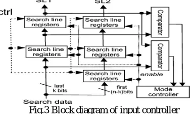
Fig.3 Block diagram of input controller
[image:3.612.212.404.603.716.2]least one of the next search words assign the same word block. Otherwise, the CAM operates at fast mode.
Fig. 3 shows the block diagram of the input controller when m is set to 2. It includes registers, a k bit comparator and a mode controller, which operates in one of two modes: fast and slow. As search words are processed before searching them in a CAM, this method can be categorized as a pre-computation method [19]. A search word is partitioned into the last k bits and the first(n-k) bits of the words. Consecutive last k bits of the current and m search words are compared to check whether they are the same or not. As long as these sub words are not the same, the input controller sends search words to the cam block at high speed.
Fig.4. CAM word circuit: (a) a NAND cell, (b) block diagram on precharge phase, (c) block diagram when a search word matches, and (d) mismatches on evaluate phase.
B. Phase-Overlapped Processing
Fig. 4 shows the block diagrams of a typical word circuit based on a NAND-type cell. Fig. 4(a) shows the circuit diagram of a typical NAND-type cell. A word line (WL) is high to write words into the cells, and is low in the search operation. The NAND-type word circuit is implemented using a series of pass transistors in the NAND-type cells. It operates in two phases: precharge and evaluate, based on dynamic logic. In the precharge phase shown in Fig. 4(b), the ML is charged through the PMOS transistor. In the evaluate phase, if a search word is the same as a stored word shown in Fig. 4(c), all pass transistors in the CAM cells are in on states. Hence, the ML capacitance is discharged. This operation is called “match”. If a search word is different from a stored word shown in Fig. 4(d), all pass transis-tors in the CAM cells are not in on states. Hence, the voltage of the ML remains high. The operation is called “mismatch.” The NAND-type word circuit reduces the power dissipation of MLs compared to the NOR-type one because only a matched circuit discharges the ML capacitance.
IV. REORDERED WORD OVERLAPPED SEARCH
A reordered word-overlapped search (RWOS) scheme to improve the throughput. It is the extension of the WOS scheme.
470
Fig.5 shows the high-level structure of the proposed CAM based on the RWOS and the POP schemes. It contains a CAM block, an input controller, and an output controller. Once input words are reordered in the input controller, the input controller sends a signal, which indicates a reordered input word to the output controller. The output controller reorders the output address based on the signal.
V. ASYNCHRONOUS CIRCUIT
Fig. 6 shows the circuit diagram of the proposed CAM word circuit based on the RWOS and POP schemes. It contains a k-bit 1st-stage sub-word circuit, a segmentation circuit, a self- precharge circuit a nd a (n-k) bit 2nd-stage sub-word circuit. The 1st-stage sub-word circuits store the last k bits of stored words and the 2nd-stage sub-word circuits store the first (n-k) bits of stored words. All CAM cells are implemented using the NAND-type cell. This circuit is implemented using asynchronous circuits [18].
The 1st-stage segment is implemented using a series of NAND type cells, a precharge PMOS transistor, and a weak feedback PMOS transistor shown in Fig. 6(a). The last k bits of a search word sent from the input controller is assigned and compared with the last of the segmentation circuit bits of stored words.The weak feedback PMOS transistor is added to the ML to solve a charge sharing problem in the NAND type cell.
The 2nd-stage segment contains the local match circuits. The local match circuit contains an inverter, precharge and weak feedback PMOS transistor, a series of k NAND type cells, and an NMOS transistor whose gate is connected as shown in Fig.6(b). All local match circuits of the word circuit operate.
All output are connected to the global match circuit. The global match circuit has a global match line (GML) that contains a series of NMOS transistors, precharge and weak feedback PMOS transistors, and an inverter shown in Fig. 6(c).
The self precharge circuit shown in Fig. 6(d) also operates. The self precharge circuit is a delay element that precharges a matched word circuit after the completion of the current search in the word circuit. In the proposed circuit, the delay element and a combinational block (sub-word circuit) are designed separately. The delay element is designed using a dummy word circuit of the sub-word circuit and several AND gates. The use of the dummy word circuit reduces the delay difference between the delay element and the sub-word circuits under voltage and temperature variations. In contrast, the previous CAM uses just AND gates as the delay element [17]. The dummy word circuit contains the same stored sub-word as that of the 1st segment of the word circuit.
Fig.6.Circuit diagram of the proposed n-bit word circuit
VI. IP FILTER
.
Fig.7 Multiple Permission IP Filter
With an IP filter, LAN users can be restricted to specific applications on the Internet (such as e-mail). CAM works as a filter to block all access except for packets that have permission. The addresses that have permission are stored in CAM; when an address is sent to memory, CAM reports whether it contains the address. If the address resides within CAM, it has permission for a particular activity. When multiple permissions are required, a combination of CAM and RAM enables this operation. A sample application that regulates access to e-mail, the web, file transfer protocol (FTP), and telnet. This application uses a 4-bit RAM block; each bit of RAM refers to one permission
Fig.9 Simulation Waveform
The simulation waveform has been shown in the Fig. 9. This waveform shows the blocked and unblocked IP address. With the help of the IP filter user can request the needed website from the server by using this filter user can unblock the blocked website. For example the user needs the E-mail and the Web the server unblocks the two IP address and permit to access the user.
VII. RESULT AND DISCUSSION
472
Fig, 8 Schematic View
In this paper, we have proposed a high-throughput low-energy content-addressable memory (CAM) based on a reordered overlapped search mechanism. The proposed CAM operates at a rate based on the short delay of the last few-bit search rather than the long delay of whole-word search. These method are realized using Asynchronous circuits. Asynchronous CAM is proposed to increase the speed of IP filter. Proposed method will reduce the power and delay decrease the total number of extra bits. So, proposed method will increase the data accuracy of the memory.
Drawback of the existing system is rectified in this method. IP filter of the proposed system is designed and implemented. The IP filter will be implemented and will be compared with existing system results.
REFERENCES
[1] S. Choi, K. Sohn, J. Ki m, J. Yoo, and H.-J. Yoo, “A TCAM -based pe-riodic event generator for multi-node management in the body sensor network,” in Proc. Asian Solid-State Circuits Conf. 2006, Nov. 2006, pp. 307–310.
[2] P.-F. Lin and J. Kuo, “A 1- V 128-kb four-way set-associative cmos cache me mory using wordline-oriented tag-compare ( WLOTC) struc-ture with the content-addressable-me mory (CAM) 10-transistor tag cell,” IEEE J. Solid-State Circuits, vol. 36, no. 4, pp. 666–675, Apr. 2001.
[3] C.-C. Wang, C.-J. Cheng, T.-F. Chen, and J.-S. Wang, “An adaptively dividable dual-port bitcam for virus-detection processors in mobile de-vices,” IEEE J. Solid-State Circuits, vol. 44, no. 5, pp. 1571–1581, May 2009.
[4] N. Onizawa, W. Gross, and T. Hanyu, “A low-energy variation-tol-erant asynchronous TCAM for network intrusion detection systems,” in IEEE 19th Int. Symp. Asynchronous Circuits Syst. (ASYNC), May 2013, pp. 8–15.
[5] N.-F. Huang, K.-B. Chen, and W.-E. Chen, “Fast and scalable multi-TCAM classification engine for wide policy table lookup,” in Proc. 19th Int. Conf. Adv. Inf. Netw. Appl., Mar. 2005, vol. 1, pp. 792–797.
[6] M. Kobayashi, T. Murase, and A. Kuriyama, “A longest prefix match search engine for multi-gigabit IP processing,” in IEEE Int. Conf. Commun. 2000, vol. 3, pp. 1360–1364.
[7] Y. Tang, W. Lin, and B. Liu, “A TCAM index scheme for IP address lookup,” in Proc. 1st Int. Conf. Commun. Netw. China, Oct. 2006, pp. 1–5.
[8] N.-F. Huang, W.-E. Chen, J.- Y. Luo, and J.-M . Chen, “Design of multi-field IPv6 packet classifiers using ternary CAM s,” in Proc. Global Telecommun. Conf., vol. 3, pp. 1877–1881.
[9] K. Pagiamtzis and A. Sheikholeslami, “Content-addressable memory (CAM ) circuits and architectures: A tutorial and survey,” IEEE J. Solid-State Circuits, vol. 41, no. 3, pp. 712–727, Mar. 2006.
[10] F. Shafai, K. Schultz, G. Gibson, A. Bluschke, and D. Somppi, “Fully parallel 30-M Hz, 2.5-Mb CAM,” IEEE J. Solid-State Circuits, vol. 33, no. 11, pp. 1690–1696, Nov. 1998.
[11] H.-Y. Li, C.-C. Chen, J.-S. Wang, and C. Yeh, “An AND-type match-line scheme for high-performance energy-efficient content addressable memories,” IEEE J. Solid-State Circuits, vol. 41, no. 5, pp. 1108–1119, May 2006.
[12] C.-C. Wang, J.-S. Wang, and C. Yeh, “High- speed and low- power design techniques for TCAM macros,” IEEE J. Solid-State Circuits, vol. 43, no. 2, pp. 530–540, Feb. 2008.
[13] I. Ar sovski, T. Chandler, and A. Sheikholeslami, “A ternary content-addressable me mory (TCAM) based on 4T static storage and including a current-race sensing sche me,” IEEE J. Solid-State Circuits, vol. 38, no. 1, pp. 155–158, Jan. 2003.
[14] I. Ar sovski and A. Sheikholeslami, “A mismatch-dependent power al-location technique for match-line sensing in content-addressable me m-ories,” IEEE J. Solid-State Circuits, vol. 38, no. 11, pp. 1958–1966, Nov. 2003.
[15] A.-T. Do, S. Chen, Z.-H. Kong, and K. S. Yeo, “A high speed low power CAM with a parity bit and power-gated ML sensing,” IEE E Trans. Very Large Scale Integr. (VLSI) Syst., vol. 21, no. 1, pp. 151–156, 2013.
IEEE J. Solid-State Circuits, vol. 39, no. 9, pp. 1512–1519, Sep. 2004.
[17] N. Onizawa, S. Matsunaga, V. C. Gaudet, and T. Hanyu, “High-throughput low-energy content-addressable memory based on self-timed overlapped search mechanism,” in Proc. 18th Int. Symp. Asynchronous Circuits Syst., May 2012, pp. 41–48.
[18] J. Sparsø and S. Furber, Principles of Asynchronous Circuit Design: A Systems Perspective [Online]. Available: books.google.com Jan. 2001 [19] K. Christensen, P. Jensen, P. Korger, and J. Sparsø, “The design of an asynchronous Tiny RISC TR4101 microprocessor core,” in Proc. 4th
Int. Symp. Adv. Res. Asynchronous Circuits Syst., Mar.-Apr. 1998, pp. 108–119.
[20] N. Onizawa, S. Matsunaga, V. C. Gaudet, W. J. Gross, and T. Hanyu, “High-throughput CAM based on a synchronous overlapped search scheme,” IEICE Electron. Exp. (ELEX), vol. 10, no. 7, p. 20130148, 2013.
[21] C. Zukowski and S.-Y. Wang, “Use of selective precharge for low- power on the match lines of content-addressable memories,” in Proc. Int. Workshop Memory Technol., Design, Testing, Aug. 1997, pp. 64–68.