ISSN Online: 2160-889X ISSN Print: 2160-8881
Numerical Simulation of an All Optical Flip-Flop
Based on a Nonlinear Distributed Bragg
Reflector Laser Structure
Hossam Zoweil
Advanced Technology and New Materials Research Institute, City of Scientific Research and Technology Applications, New Borg EL-Arab City, Alexandria, Egypt
Abstract
A new design for an all optical flip flop is introduced. It is based on a nonlinear Dis-tributed Bragg Reflector (DBR) semiconductor laser structure. The device does not require a holding beam. An optical gain medium confined between 2 Bragg reflectors forms the device. One of the Bragg reflectors is detuned from the other by making its average refractive index slightly higher, and it has a negative nonlinear coefficient that is due to direct absorption at Urbach tail. At low light intensity in the structure, the detuned Bragg reflector does not provide optical feedback to start a laser mode. An optical pulse injected to the structure reduces the detuning of the nonlinear Bragg reflector and a laser mode builds up. The device is reset by detuning the second Bragg reflector optically by an optical pulse that generates electron-hole pairs by di-rect absorption. A mathematical model of the device is introduced. The model is solved numerically in time domain using a general purpose graphics processing unit (GPGPU) to increase accuracy and to reduce the computation time. The switching dynamics of the device are in nanosecond time scale. The device could be used for all optical data packet switching/routing.
Keywords
All-Optical Flip-Flop, Distributed Bragg Reflector, Nonlinear Grating, GPGPU
1. Introduction
All-optical flip-flops are building blocks in all optical network. All-optical flip-flop is used as an all optical memory element, or in all optical signal processing/generation, [1] [2]. Several devices/systems are introduced to perform all-optical flip-flop function. An How to cite this paper: Zoweil, H. (2016)
Numerical Simulation of an All Optical Flip-Flop Based on a Nonlinear Distributed Bragg Reflector Laser Structure. Optics and Photonics Journal, 6, 217-228.
http://dx.doi.org/10.4236/opj.2016.69023
Received: August 22, 2016 Accepted: September 27, 2016 Published: September 30, 2016
Copyright © 2016 by author and Scientific Research Publishing Inc. This work is licensed under the Creative Commons Attribution International License (CC BY 4.0).
all-optical flip-flop based on 2 semiconductor lasers is shown in [3], the lasers are coupled such that when one laser is “ON” it quenches the other. A device based on coupled micro ring lasers is presented in [4], the device is implemented on an InP/InGaAsP photonic integrated circuit. The two output states of the flip-flop are due to clock-wise and anti-clock-wise laser modes in the coupled rings. Low power device where the two output states are clock-wise and anti-clock-wise laser modes in a single micro disk laser is implemented on a silicon chip in [5]. A device based on Distributed Feedback (DFB) semiconductor laser and a holding beam is shown in [6], where the bistability is due to spacial hole burning effect. In [7], an all optical flip-flop based on dispersive bistabolity in Vertical Cavity Semiconductor Optical Amplifier (VCSOA) is implemented. The device is reset by cross gain modulation (XGM) in the presence of a holding beam. These devices require holding beams or they generate output at both states, other types of devices are bistable laser diodes. The bistable laser diode does not require a holding beam. The bistable laser diodes have two states; OFF states (no optical output), or ON state. In [8][9], a saturable absorber is implemented within the gain la-ser cavity to achieve optical bistability, in a bistable lala-ser diode. In [10][11], bistable la-ser diodes are investigated. The optical bistability is due to nonlinear distributed optical feedback within the laser cavity.
In [11], a bistable all optical flip-flop is introduced. The device consists of a DFB laser structure, where a part of the wave-guiding layer is detuned from the remaining part of the DFB structure. The detuned part has a negative nonlinear coefficient such that at a high light intensity in the structure the negative nonlinear coefficient reduces the de-tuning of the DFB section. Whence the dede-tuning is reduced, the optical feedback along the structure allows for a laser mode to build up. The laser mode light intensity main-tains the detuning in the nonlinear section. The Device is switched OFF by another optical pulse of higher frequency that is able to detune a second part of the DFB wave-guiding layer (by generating electron-hole pairs that reduce the average refractive index in that section). To prevent the Reset pulse from reaching the nonlinear part of the structure, an optical loss section that absorbs the optical signal in the range of the reset pulse frequency is introduced in the structure to attenuate the reset pulse before reaching the nonlinear detuned section.
The device has a simple design, compared to the device shown in [11]. The switch OFF dynamics in [11] depends on cross gain modulation (XGM), where a Reset pulse at a frequency higher than the operating wavelength reduces the optical gain, and the laser mode is switched OFF. The switch OFF mechanism in this work depends on re-ducing the quality factor (by rere-ducing the optical feedback from one of the DBR sec-tions) of the laser cavity optically. The optical gain is not altered by the Reset pulse.
In the following sections, the operation and the schematic of the device are described in details. Also, a mathematical model describing the device is introduced. The mathe-matical model is solved numerically, and results are plotted and discussed.
2. Device Configuration and Operation
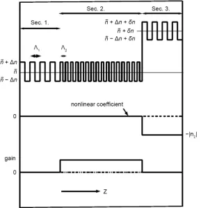
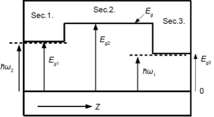
The device is shown in Figure 1. It consists of a distributed Bragg reflector section (sec-tion “1”), followed by a gain sec(sec-tion (sec(sec-tion “2”), and a nonlinear distributed Bragg reflector (section “3”) that is detuned from the Bragg reflector of section “1”.
In section “1”, 2nΛ =1 λG =λ1, where n is the average refractive index, Λ1 is the grating period. λG1 is the wavelength at the center of the reflection band. λ1 is assumed
to be 1500 nm. λ1 presents the set pulse wavelength. The optical gain spectrum of
sec-tion 2 has its peak gain around λ = λ1. In section 2, 2nΛ =2 λG2 =λ2. λG2 is the wave-length at the center of the reflection band of the grating in section “2”. Λ2 is the grating
[image:3.595.232.522.389.689.2]period in section “2”. λ2 = 1400 nm which is the reset pulse wavelength.
Switching Dynamics
At low light intensity in the structure, due to the detuning of section “3”, lacking of optical feedback will prevent the laser mode from building up. By injecting an optical pulse at λ = λ1 (at z = 0), the detuning of section “3” is reduced due to the negative
non-linear coefficient. The negative nonnon-linear coefficient in section “3” is due to direct ab-sorption at Urbach tail, [12][13]. It is assumed that the photon energy at λ = λ1 is few
tenths of Milli-electron.volts (meV) below the band-gap energy in section “3”. In this case, the reflections bands of gratings in sections “1” and “3” start to overlap. This overlap provides optical feedback that allows for a laser mode to build up. The laser mode intensity maintains the reduction in the detuning of section “3”, and the output laser mode is stable.
To reset the device (to switch the laser output OFF), section “1” is detuned optically. The optical Reset pulse reduces the refractive index in section “1” by direct absorp-tion at the Urbach tail in secabsorp-tion “1”. It is assumed that the photon energy at λ2 is few
tenths of Milli-electron.volts (meV) lower than the band gap energy of section “1”. Re-duction of refractive index in section “1” leads to the detuning of the grating in section “1”. Hence the reflections bands of sections “1” and “3” do not overlap, and the optical feedback does not support optical laser mode anymore. The laser mode ceases to exist and the average refractive index in section “3” relaxes to its original value which leads to the detuning of grating in section “3”. The Reset pulse at λ = λ2 may generate
elec-tron-hole pairs in section “3” too. To avoid this, a grating in section “2” is introduced (as shown in Figure 2), this grating reflects the Reset pulse back to section “1”. The grating reflection band is around λ = λ2, and the reflection band is chosen to be outside
the gain spectrum of the active region in section “2”. In the simulations, it is assumed that λ2 = 1400 nm. The semiconductor band gaps in sections “1”, “2”, and “3” could be
adjusted to match the Set and Reset pulse incident photon energies by fabricating the waveguide from semiconductor alloy InGaAsP on InP substrate. By changing the per-centages of the elements of the alloy InGaAsP, the band gap of the semiconductor changes, [14].
[image:4.595.267.482.555.673.2]In the following section, a mathematical model of the device is presented, and the simulation parameters are tabulated and discussed.
3. Mathematical Model and Simulation Parameters
The optical field inside the structure is assumed to consist of a forward propagating mode and a backward propagating mode. Slow wave approximation is assumed, [15].
The electric field at λ = λ1 (ω = ω1) is:
( )
,( )
, exp[
]
( )
, exp[
]
. .E z t =E+ z t i zβ −i tω +E− z t −i zβ −i tω +c c.
It presents both the Set pulse and the output optical field. The Reset pulse is modeled as:
( )
, Reset ,Reset( )
, exp[
2]
,Reset( )
, exp[
2]
. .E z t =E+ z t i zβ −iω t +E− z t −i zβ −iωt +c c .
It is modeled at ω = ω2 (λ = λ2). The mathematical model of the Flip-Flop is presented
through the following equations:
( )
(
)
(
( )
[
]
)
1 1 2 exp 2
2 2
cav
E n E g
i z i E i z i z E
z c t
α
γ δβ
+ +
+ −
∂ + ∂ = Γ + + − + Γ
∂ ∂ (1)
( )
(
)
(
( )
[
]
)
1 1 2 exp 2
2 2
cav
E n E g
i z i E i z i z E
z c t
α
γ δβ
− −
− +
∂ − ∂ = − Γ + + − − Γ −
∂ ∂ (2)
( )
[
]
(
)
, ,
, 3 exp 2 ,
2 2
Reset Reset abs cav
Reset Reset
E n E
E i z i z E
z c t
α α δβ
+ +
+ −
∂ + ∂ = − − + Γ
∂ ∂ (3)
( )
[
]
(
)
, ,
, 3 exp 2 ,
2 2
Reset Reset abs cav
Reset Reset
E n E
E i z i z E
z c t
α α δβ
− −
− +
∂ − ∂ = − Γ −
∂ ∂ (4)
( )
(
)
(
)
1 1 , 2π d 1d c 2
G
z n
n z N i i
N
α ω
δ ξ
λ
Γ = − − +
(5)
2 1
4
, for 0 4 , and for 3 4 .
G
n z L L z L
λ
Γ = ∆ < < < < (6)
3 2
4
, for 4 3 4.
Reset G
n L z L
λ
Γ = ∆ ≤ ≤ (7)
( )
, 2 3(
, 1)
1(
, 2)
2c c abs
c c
c
N z t N z I z I
BN CN
t
α ω α ω
τ ω
∂ +
= − − − +
∂ (8)
( )
current 2 3( )
1 1
,
g g
g g g
g
N z t I N
BN CN v g S
t qV τ ω
∂
= − − − − Θ
∂ (9)
( )
( )
(
)
1
g tr
g N N
g S ω ω ε − = + (10)
Equations (1) and (2) present the forward and backward waves of the laser mode. Equations (3) and (4) present the forward and the backward waves of the input Reset pulse. c is the velocity of light in vacuum. n is the average refractive index of
wave-guiding layer. L = 187.5 μm is the length of the structure. δn = 0.006 in section “3”. δβ is the detuning of the incident light from the grating’s center wavelength. It is chosen to be δβ = 0 in the simulations.
Γ1 presents the detuning in section “3” and the direct absorption loss at that section. dndN
− = −10−26 m3 presents the change in the refractive index due to the change in
loss introduced by the free carriers generated in the semiconductor, [16][17]. In sec-tion 3, α (z) = 480 cm−1, which is the direct absorption at λ
1. Γ2 is the coupling
coeffi-cient in section “1” and “3”. Δn = 0.001. Γ3 is the coupling coefficient in section “2”.
ΔnReset = 0.06. The direct absorption loss in section “1” is αabs = 480 cm−1 at λ = λ2. Nc is
the generated electron-hole carriers density in the semiconductor guiding layer along the device. I1 is the optical power density in Watt/meter2 of the switched laser mode. I2
is the optical power density of the Reset pulse in Watt/meter2. N
g is the electron-hole
density in the active gain layer that provides gain in section “2”. q is the electron charge, and V is the volume of the active gain cavity.
Other simulation parameters are shown in Table 1.
The coupled differential equations are solved numerically using Rung-Kutta tech-niques. To increase the numerical accuracy and to reduce the computing time, a gener-al purpose graphics processing unit (GPGPU) is used in the simulation to perform pa-rallel computing of the system of the differential equations. A PC machine is used to perform the simulations. It is built with: GTX 980Ti GPU card, 32 GB RAM, operating system Linux (Ubuntu), and processor Intel @ CoreTM i3-4130 CPU @ 3.40 GHz × 4.
The integration step used in the z direction is L/80. The time integration step is
80
nL c . After each integration step in time domain, random optical fields are added to the forward and backward laser mode fields to simulate the spontaneous emission from the active layer. In each time integration step, the integration along the z direction is performed by 80 parallel threads on the GPU card. The simulation code is written using CUDA C, [18]. In the following section simulation results are presented and discussed.
Table 1. Device parameters.
Symbols Description Value
L Length 187.5 μm
Icurrent Current injected in the active layer 0.13 Ampere
vg Group velocity 108 m/sec
γ Line-width enhancement −0.5
Gain saturation 1.5 × 10⁻²³ m3
Θ Overlap factor 0.35
V Cavity volume 0.18 × 10⁻¹⁶ m3
τcar Non-radiative recombination in nonlinear sections 1 nsec
τg Non-radiative recombination in the active layer 3 nsec
B Radiative Recombination 10−23 m3/sec
C Auger recombination 3 × 10−40 m6/sec
( )1
g ω Differential gain at ω1 4 × 10⁻²⁰ m2
4. Simulations and Results
In the following simulations, the laser output mode power, and the Reset pulse optical power are both normalized to P0 = 5 × 10⁻⁵ Watt. The electron-hole pairs density
gen-erated in the nonlinear wave-guiding layer is normalized to Nc = 1023 m−3. The
elec-tron-hole carrier density in the active layer Ng is normalized to Ntr. Also, the coordinate
z along the device is normalized to L. The time step in the integration is normalized to
80
nL c .
4.1. Optical Bistability Loop Simulation
In order to estimate the injected current that will lead to a bistable operation of the de-vice, the optical bistability loop should be simulated numerically. This is performed by increasing the current injected to the device from zero to 197 mA linearly in 150 nsec, then, the injected current is decreased linearly to zero in another 150 nsec. The output optical power is plotted against injected current. A part of the optical bistability loop is shown in Figure 3. The extinction ratio between ON and OFF state is
(
)
10
10 log PON POFF 150 dB. From the bistability loop, an injected current of I = 130
mA is assumed as it allows for a bistable operation.
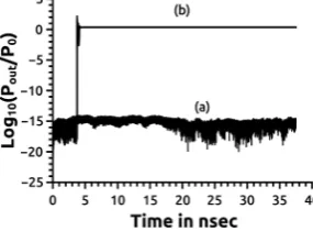
4.2. Simulations of Steady States: OFF and ON States
In Figure 4, the output optical power is simulated for 37.5 nsec during OFF state. The output optical level corresponds to amplified spontaneous emission at z = L. To switch the device ON, an optical pulse at wavelength λ = λ1 and optical power P = P0 is injected
[image:7.595.298.446.438.548.2]at z = 0. The optical pulse is injected at simulation time t = 3.75 nsec, and has a width of
[image:7.595.301.444.586.691.2]Figure 3. Bistability loop versus injected current.
0.1875 nsec (pulse energy 9.34 × 10⁻³ Picojoule). It generates electron-hole pairs in
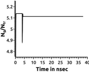
sec-tion 3 by direct absorpsec-tion of photons at Urbach tail. The free carriers density reduces the refractive index in section “3”. The detuning in section “3” is reduced and the ref-lection bands of both gratings (in section “1” and “3”) overlap. This overlap provides optical feedback to build up a laser mode. The optical intensity of the laser mode main-tains the electron-hole carriers density in section “3” (as a part of the laser mode is ab-sorbed in this section), and the output laser mode is stable. The optical laser output sta-bilizes in about 0.5 nsec. Nc N0, the normalized electron-hole density at z = 7L/8 in section "3" is plotted as function of time in Figure 5. Nc N0 increases by the injection of the optical pulse, then it stabilises at Nc N05. Ng Ntr , the normalized carrier density in the active gain layer at z = L/2 is plotted as function of time in Figure 6.
g tr
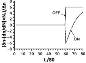
N N is reduced slightly in the ON state, this is because small output laser power is enough to maintain the reduction in refraction index in section “3”. Figure 7 shows the normalized change in the average refractive index along the device. That is
(
δ −n d dn N×Nc)
∆n is plotted against z for both the OFF state, and ON state at the end of the simulation time (at t = 37.5 nsec).4.3. Simulations of ON/OFF Transition Dynamics
[image:8.595.301.449.390.502.2]In this section, the ON/OFF transitions dynamics are investigated in time domain. First the device is switched ON by an input optical pulse injected at z = 0. At t = 0.75 nsec
Figure 5. Nc/N0 at z = 7L/8 as a function of time
during ON state operation.
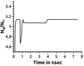
Figure 6. Ng/Ntr at z = L/2 as a function of time
[image:8.595.296.450.551.677.2]Figure 7. Normalized change in refractive index along z in: (a) OFF state, and (b) ON state.
from the beginning of the simulation time, an input pulse at λ = λ1, of width 0.1875
nsec (9.34 × 10⁻³ Picojoule) is injected to the device. The injected pulse induces free
carriers in section “3” and reduces the refractive index. Hence the reflection bands of grating in sections “1” and “3” overlap and the optical feedback allows for a laser mode to build up. A part of the laser mode intensity is absorbed in section 3, and it maintains the electron-hole density required to reduce the refractive index in section 3. To switch the device OFF, an optical pulse at λ = λ2 is injected to the device at z = 0. The optical
pulse has power PReset = P0, and it is injected at time t = 3.75 nsec. The pulse has a width
of 0.46875 nsec (pulse energy = 0.0234 Picojoule). The injected pulse has photons energy slightly less than the band gap energy of section “1”. A part of the pulse photons are absorbed at Urbach tail in this section. The electron-hole generated in section “1” reduces the refractive index in this section. When the refractive index in section “1” is reduced, the reflection bands of both gratings in sections “1” and “3” do not overlap any more. No optical feedback can sustain the laser mode. The laser mode is switched OFF, and the refractive index in section 3 starts to relax to its original value in the OFF state. The output optical power is shown in Figure 8 during ON and OFF operations/ transitions. The laser output transition from OFF to ON state stabilizes in about 0.5 nsec. The laser mode is switched from ON state to OFF state in about 0.32 nsec.
0 c
N N at z = 7L/8 is shown in Figure 9 as a function of time. Ng Ntr at z = L/2 is shown in Figure 10 as a function of time. The Reset pulse width 0.46875 nsec is longer than the Set pulse width. The slightly longer pulse width is needed to allow for Nc in
section “3” to decay during the Reset pulse so that when the Reset pulse elapses, the optical feedback from section 3 does not allow for the laser mode to build up again. The optical Reset pulse at λ = λ2 can generate electron-hole pairs in section “3” if it reaches
this section. In order to prevent the Reset pulse from reaching section 3, the grating in section “2” is introduced to reflect this pulse back to section “1”. ΔnReset is chosen to be
0.06 in section “2” to produce a strong coupling between forward and backward wave at λ = λ2 in this section which results in a very small percentage of the Reset pulse is
reaching section “3”. Figure 11 shows the Reset pulse power at z = 3L/4; at the end of section “2” as a function of time. The Reset pulse power reaching this section is about PReset × 10−12, the attenuation is due to the direct absorption in section “1”, and the
The relative change in the average refractive index in both sections “1” and “3” dur-ing ON/OFF transitions is plotted as a function of distance along the device at several time frames as shown in Figure 12.
[image:10.595.302.449.278.382.2]Figure 8. Output optical power during ON/OFF operations.
Figure 9. Nc/N0 at z = 7L/8 evolution with time
during ON/OFF operations.
Figure 10. Time evolution of Ng/Ntr at z = L/2
during ON/OFF operations.
[image:10.595.303.446.422.534.2] [image:10.595.300.447.575.679.2]Figure 12. Refractive index changes along the structure at different time frames.
5. Discussion
The switch OFF time of the device is about 0.32 nsec, which is small compared to the switch OFF time of 2 nsec of the flip-flop in [11]. The injected current in [11] is 0.95523 Amp, but in this work the injected current is 0.13 Amp for the same device length. In this work, the need for an optical absorber as in [11] is eliminated by using a strong grating at the middle of the device to prevent the reset pulse from reaching the nonli-near section. The device could be built from InGaAsP alloy on InP substrate to be able to alter the bandgap along the structure. However it is possible to build the device from 3 separate section: DBR section, a gain section with a strong grating tuned to λ = λ2 and
a nonlinear DBR section.
6. Conclusion
In this work, a new semiconductor all-optical flip-flop is introduced. The device is a bistable laser diode, and it does not require a holding beam for a bistable operation. The device consists of DBR laser with a nonlinear DBR section. The nonlinearity is due to direct absorption at the Urbach tail. A mathematical model that describes the fields and carriers density in the device is presented. The mathematical model is solved numeri-cally using parallel computing on a GPGPU to reduce the simulation time and to in-crease the accuracy. The all optical flip-flop presented in this work is a single bistable laser diode, however it is possible to implement the device from three separate devices (2 DBR sections and one gain section) The investigation of such possible design will be left for a future work. The device could be implemented using InGaAsP alloy on InP substrate. The output optical field in OFF to ON state transition is stabilised after 0.5 nsec, and the ON to OFF state transition takes about 0.2 nsec. The switching dynamics are in nano-second time scale. The device is suitable for applications such as all-optical data packet routing/switching.
References
[1] Dorren, H.J.S., Hill, M.T., Liu, Y., Calabretta, N., Srivatsa, A., Huijskens, F.M., de Waardt, H. and Khoe, G.D. (2003) Optical Packet Switching and Buffering by Using All-Optical Signal Processing Methods. Journal of Lightwave Technology, 21, 2-12.
[2] Li, P., Wang, Y. and Zhang, J. (2010) All-Optical Fast Random Number Generator. Optics Express, 18, 20360-20369. http://dx.doi.org/10.1364/OE.18.020360
[3] Martin, T., de Waardt, H., Khoe, G.D. and Dorren, H.J.S. (2001) All-Optical Flip-Flop Based on Coupled Laser Diodes. IEEE Journal of Quantum Electronics, 37, 405-413. http://dx.doi.org/10.1109/3.910450
[4] Hill, M.Y., Dorren, H.J.S., de Vries, T., Leijtens, X.J.M., den Besten, J.H., Smalbrugge, B., Oei, Y.S., Binsma, H., Khoe, G.D. and Smit, M.K. (2004) A Fast Low-Power Optical Mem-ory Based on Coupled Micro-Ring Lasers. Nature, 432, 206-208.
http://dx.doi.org/10.1038/nature03045
[5] Liu, L., Kumar, R., Huybrechts, K., Spuesens, T., Roelkens, G., Geluk, E.J., de Vries, T., Re-greny, P., Thourhout, D.V., Baets, R. and Morthier, G. (2010) An Ultra-Small, Low-Power, All-Optical Flip-Flop Memory on a Silicon Chip. Nature Photonics, 4, 182-187.
[6] Huybrechts, K., Morthier, G. and Baet, R. (2008) Fast All-Optical Flip-Flop Based on a Sin-gle Distributed Feedback Laser Diode. Optics Express, 16, 11405-11410.
http://dx.doi.org/10.1364/OE.16.011405
[7] Kaplan, A.M., Agrawal, G.P. and Maywar, D.N. (2009) All-Optical Flip-Flop Operation of VCSOA. Electronics Letters, 45, 127-128. http://dx.doi.org/10.1049/el:20093124
[8] Kawaguchi, H. (1997) Bistable Laser Diodes and Their Applications: State of the Art. IEEE Journal of Selected Topics in Quantum Electronics, 3, 1254-1270.
[9] Odagawa, T. (1991) Bistable Semiconductor Laser Diode Device. US Patent, 5007061. [10] Zoweil, H. (2015) Numerical Simulation of a Novel All-Optical Flip-Flop Based on a
Chirped Nonlinear Distributed Feedback Semiconductor Laser Structure Using GPGPU Computing. Journal of Modern Optics, 62, 738-744.
http://dx.doi.org/10.1080/09500340.2015.1005186
[11] Zoweil, H. (2016) Simulations of an All-Optical Flip-Flop with a Reset Pulse Frequency Ex-ceeding Operating Frequency. Egyptian Journal of Basic and Applied Sciences, 3, 322-328. http://dx.doi.org/10.1016/j.ejbas.2016.04.001
[12] Pankove, J.I. (1965) Absorption Edge of Impure Gallium Arsenide. Physical Review, 140, A2059-A2065. http://dx.doi.org/10.1103/PhysRev.140.A2059
[13] Dow, J.D. and Redfield, D. (1972) Toward a Unified Theory of Urbach’s Rule and Expo-nential Absorption Edges. Physical Review B, 5, 594-610.
[14] Adachi, S. (2004) Physical Properties of III-V Semiconductor Compounds. Wiley, Hobo-ken. (Nostrand Reinhold, 1993)
[15] Carrol, J., Whiteaway, J. and Plumb, D. (1998) Distributed Feedback Semiconductor Laser. IEE, London. http://dx.doi.org/10.1049/PBCS010E
[16] Bennett, B.R., Soref, R.A. and Del Alamo, J.A. (1990) Carrier-Induced Change in Refractive Index of InP, GaAs, and InGaAsP. IEEE Journal of Quantum Electronics, 26, 113-122. http://dx.doi.org/10.1109/3.44924
[17] Haug, H. (Ed.) (1988) Optical Nonlinearities and instabilities in Semiconductors. Academic Press, INC. New York.
Submit or recommend next manuscript to SCIRP and we will provide best service for you:
Accepting pre-submission inquiries through Email, Facebook, LinkedIn, Twitter, etc. A wide selection of journals (inclusive of 9 subjects, more than 200 journals)
Providing 24-hour high-quality service User-friendly online submission system Fair and swift peer-review system
Efficient typesetting and proofreading procedure
Display of the result of downloads and visits, as well as the number of cited articles Maximum dissemination of your research work