Instruction-Reference
Preface
This publication, Form 223-2589, obsoletes and con-tains information formerly found in the following Cus-tomer Engineering Instruction-Reference manuals: IB M
1410 System Fundamentals and 1411 Functional Units,
Form R23-2589; IBM 1410 Component Circuits, Form R23-9776; IBM 1410 Timing Charts and Second Level
Diagrams, Form R23-9774-1; and IBM 1410 Data
Proc-essing System, Form 225-6549-l.
The information formerly contained in the 1410 Sys-tem Fundamentals and 1410 Component Circuits man-ual remains unchanged, but the 1410 Timing Chart and Second Level Diagrams manual has been revised. The revised portion eliminates many diagrams that can now be found in their related manuals. For example, dia-grams for Input-Output or Console Operations can be found in IBM 1410 Input-Output Operations, Form R23-2692, or in IBM 1415 Console, Form R23-2648.
Copies of this and other IBM publications can be obtained through IBM Branch Offices. Address comments concerning the contents of this publication to:
IBM Corporation, CE Manuals, Dept. B96, PO Box 390, Poughkeepsie, N.Y.
System Fundamentals.
Operation of Functional Units
Operating Fundamentals of a Computer System 1410 Components
IBM 1411 Processing Unit
IBM 1414 Input-Output Synchronizer
IBM 1415 Console and Input-Output Printer
IBM 1402 Card Read Punch
IBM 1403 Printer
IBM 729 and 7330 Magnetic Tape Units
IBM 1405 Disk Storage IBM 1301 Disk Storage
IBM 1412 and IBM 1419 Magnetic Character Readers IBM 7750 Programmed Transmission Control IBM 1009 Data Transmission Unit
IBM 1011 Paper Tape Reader
IBM 1014 Remote Inquiry Unit Program Addressable Clock Telegraph Input-Output 1410 Fundamentals
Machine Language
Packaging and Component Parts Storage Principles
Stored Programming . Control
Data Flow ..
1411 Functional Units . .
Control Unit .. Logic Clock Cycle Control Address Unit
Address Registers ... . Address Modification
Address Exit-Channel Validity Check Address-Channel Validity Check Operational Unit
B Data Register ... . B Register Set Check
B Channel ... . B Character Select Check
B Channel Validity Check ... . A Data Register
A Register Set Check .. . . ... . A Channel.
A Character Select Check A Channel Validity Check Assembly
Assembly Channel Validity Check ... . Adder
Compare Unit ... Instruction Read-Out
Operating Principles Op Register Set Check Op Modifier Register Set Check Instruction Check
Address Check ... . Indexing ...
Operating Principles 7 7 8 8 8 8 8 8 8 9 9 9 9 9 9 9 9 10 10 10 10 12 12 13 13 14 17 17 17 20 21 22 22 27 27 27 28 28 29 29 29 31 31 31 32 33 33 36 36 39 41 41 52 53 53 54 54 56 Contents Power Supplies. Regulation
Special-Voltage Power-Supply Unit Power-On Sequence
Emergency Off Dc-Off Power-Off
Local Remote Operation - 1-0
TAU Off-Line Operation - Local Remote Switch 1301 File Control Unit (FCU) Off-Line
Operation-Local-Remote
1405 FCU Off-Line Operation Power-Fault Indicators
Thermal Reset Overcurrent Failure Overvoltage Failure
Marginal Checking ... . Portable Marginal-Check Power-Supply Unit Power Unit Locations
Frame and Chassis Designations
Component Circuits
Logic Families ... . Automated Logic Diagrams
Line Levels .. ... . Basic Circuits ... .
Positive AND - Negative OR (SDTRL)
Negative AND - Positive OR - Inverter (SDTDL) Trigger (SDTDL) ... . Emitter Follower (SDTRL)
Single Shot (SDTRL) Drift Sense Amplifier Card Descriptions
DFK DFS DFV
DFW . . . . DFY . . . . DFZ . . . . DGK . . . . DGM . . . . DHE . . . . DHN . . . . KG . . . .
86
86
86 86 86 86 86 88 88 88 88
TAM . . . 88
Reference Information ... . IBM 1411 CE Console ... . Address Display ... . B Character Select Switch ... . Portable Controls ... . Address Stop and Scope Sync ... . System Voltages ... . IBM 1411 Voltages ... . IBM 1414A Voltages ... . TAU Voltages ... . IBM 1405 Voltages ... . 96 96 96 96 96 96 96 96 96 98 98 Check Test ... 98
Procedure ... 98
Marginal Voltage Tests ... 98
Marginal Frequency Test ... 100
Single Shot ... 100
IBM 1411 Timings ... 100
IBM 1402-2 Attachment Timings ... 101
IBM 1403 Attachment Timings ... 101
Tape Adapter Unit Timings ... 101
IBM 1011 Attachment Timings ... 101
Delay Lines ... 101
Service Aids ... 101
General ... ,... 101
Operations ... 102
1-0 Printer . . . 102
Card Read-Punch Operations ... 103
IBM 1403 Printer Operations . . . .. 103
Magnetic Tape Operations 103 Locations and Voltage Changes. . . . 103
Component Locations ... 103
Input Voltage Change ... 103
FIGURE TITLE PAGE
1. Operation of Functional Units . . . 7
2. Synchronizer Models Required for Each 1-0 Device. 8 3. Standard BCD Interchange Code ... . . . .. 11
4. Two-Out-of-Five Code. . . .. 12
5. Qui-Binary Code ... . . . . . . .. 12
6. Instruction Phase . . . .. 14
7. Data Flow ... 15
8. CPU Data Flow . . . .. 16
9. Logic Clock ... 18
10. Logic Clock Pulses and Gates . . . .. 18
11. 1410 CPU Clock Control. . . .. 19
12. Compute Disable Cycle . . . .. 20
13. Overlap . . . .. 20
14. Logic Clock Pulse Timings. . . . .. 21
15. Control Latches . . . .. 21
16. Address Register Latch (14.11.03) ... 22
17. Address Modify Operation. . . . .. 23
18. Address Modification of ARR . . . .. 24
19. Address Modify Latches. . . .. 25
20. Address Modify Timing . . . . . . . .. 26
21. Address Exit Channel Validity Check (18.14.02) ... 27
22. Address Channel Validity Check (18.14.03) ... 28
23. Operational Unit ... 28
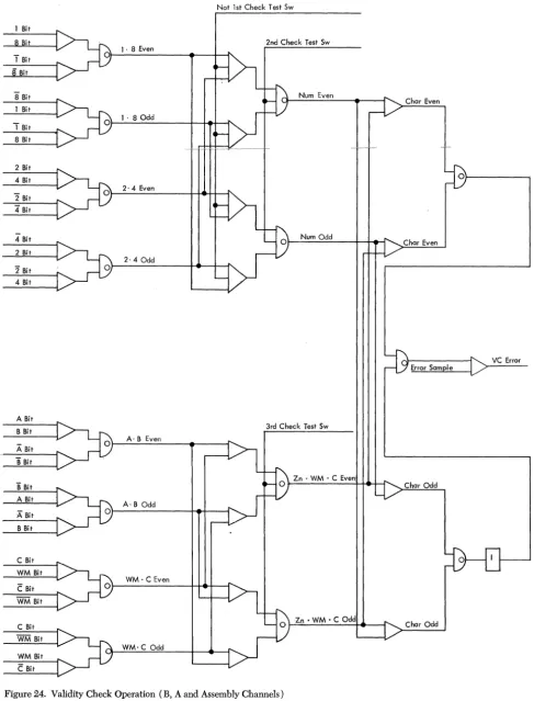
24. Validity Check Operation (B, A, and Assembly Channels) ... 30
25. A Data Register Reset and Switching . . . .. 31
26. A Register Set Check (18.14.07) ... 32
27. A Channel Gating (15.38.02 and 03) ... 32
28. A Character Select Check (18.14.01) ... 33
29. A Channel Validity Check (18.11.01-03) ... 34
30. Assembly Operation ... 34
31. Numeric Assembly 4 Bit (15.50.03) ... 35
32. Zone Assembly A Bit (15.50.05) ... 35
33. WM Assembly (15.50.08) ... 35
34. Numeric C Bit Assembly (15.50.09) ... 36
35. Zone C Bit Assembly (15.50.10) ... 36
36. C Bit Assembly (15.50.07) ... 37
37. Adder Operation ... 38
38. True Complement Controls (16.20.12) .. . . 39
39. Qui-Binary Combination. . . .. 39
40. 1410 Adder ... 40
41. Collating Sequence ... 41
42. Compare Unit Operation (17.15.01-07) ... 42
43. Instruction Read-Out Operation (Sheets 1-3) .... 43-45 44. Instruction Read-Out Timings ... 46
45. I Phase Latches . . . .. 47
46. IBM: 1410 Common Op Code Grouping Lines (13.14.01-14) ... 49
47. Op Register Set Check (18.14.04) ... 53
48. Op Mod Register Set Check (18.14.05) ... 53
49. Op Code Lengths ... 54
50. Instruction Check ... 55
51. Address Check (18.14.11) ... 56
52. Index Register Locations ... 57
53. Index Tag ... 57
54. Indexing Operation ... 58
55. indexing Timings . . . .. 59
56. IBM 1410 Power Distribution 62 57. Power-On Timing Chart .... : : : : : : : : : : : : : : : : : : :: 63
58. Power On . . . 64
59. DC Off Timing Chart . . . 65
60. DC Off .. . . .. 66
Illustration List
FIGURE TITLE
61. Input-Output Synchronizer (Power On) ... . 62. Power On, Tape Units ... . 63. Power On, File Units (1301 Only) ... . 64. Marginal-Check Power Supply (Portable Unit) ... . 65. Marginal-Check Unit in Series with SMS Power
Supply ... . 66. IBM 1411 A Frame Front ... . 67. IBM 1411A Frame Rear ... .
68. Frame and Chassis Designation ... . 69. Two Logic Families in One Operation ... . 70. Typical 1410 Automated Logic Diagram ..
71. Multiple Outputs-Same Line Name ... . 72. Logic Block Format ... . 73. Typical 1410 Logic Block ... . 74. Logic Block Pin Connections ... . 75. Extender Application ... . 76. Limiters (Terminators) ... . 77. Dot Functions ... . .
78. NOR and NAND Driving Requirements .. .
79. Line Characteristics . . . . ... . 80. SDTRL Positive AND-Negative OR ... . 81. SDTDL Negative AND - Positive OR - Inverter
(Single Level) ... . 82. SDTDL Trigger ... . 83. SDTRL Emitter Follower ... .
84. SDTRL Single Shot ... . 85. Drift Sense Amplifier ... .
86. ABN Card ... . 87. AEK Card ... .
88. CD Card
89. CRZV Card ... . 90. DBX Card
91. DEA Card. . . . ... . 92. DED Card .. ... . ... .
93. High and Low Speed SDTDL Circuits .. 94. SDTDL Circuits ... .
95. DEM Trigger ... . 96. DEM Timings .. . ... .
97. DEQ Card ... . ... . 98. DEY Card
99. DEY Card Timings .. 100. DEZ Card ....
101. DEZ Timings. . . . ... . 102. DFK Card ...
103. DFS Low Power Inverter 104. DFV Memory Driver ... . 105. DFW Memory Inhibit Driver 106. DEY Power Gate ... .
107. DFZ Cable Terminator . . . . ... . 108. DGK Delay Line . . . ... . 109. DGM Card ... . 110. DHE Single Shot ... . 111. DHN Card ... . 112. KG Card . . . . ... . 113. TAM Logic ... . 114. TAM Timings ... . 115. IBM 1411 CE Panel ... . 116. Address Stop or Scope Sync ... . 117. 1411 CE Panel Address Stop and Keyboard Control 118. Laminar Bus Pin Locations
119. IBM 1405 and 1414A Powe~~S~~~i; L~c~i:io~s' : : : : : 120. Frame Designation Large Chassis (Wiring Side) ..
FIGURE TITLE PAGE
121. Frame Designation, Tape Adapter Unit (Wiring
Side) ... 104
122. Frame Designation, I/O Synchronizer (Wiring Side) ... 104
123. 1410 Second Level Diagram Configurations ... 105
124. ADDRRegisters Read-Out CTRLS ... 105
125. Address Register Sets and Resets . . . .. .. 106
126. AAR, BAR, CAR, DAR, and IAR Latches ... 107
127. AR Bus and MEM AR to IAR Latches ... 108
128. Address Modification ... 109
129. ADDR REG CTRLS, ADDR Bus Gated, ADDR EX CH and EX CHK . . . .. 110
130. Cycle CTRLS, Cycle Length CTRLS, and Special Logic Gates ... . . . .. III 131. A and I Ring Controls ., . . . .. 112
132. A and B Cycle Controls ... . . . .. 113
133. C, D, I, X Cycle Controls ... . . .. 114
134. Scan Controls and Latches ... 115
135. Units, Body, Extension, MQ Controls, and Divide and Arith Overflow Latches ... 116
136. Address Channel Controls, Last Execute Cycle, Bal-ance Zero and Sign Controls, and Latches .... . .. 117
FIGURE TITLE PAGE 137. A and B Bits, Drives and Channel Characters 118 138. Branch Conditions ... 119
139. 1401 Branch and No Branch Conditions ... 120
140. Edit Translator and Controls ... . . .. 121
141. Edit Latches ... 122
142. Edit Controls ... . . . .. 123
143. Indexing ... 124
144. 16K Zone Adder and Grouping . . . .. 125
145. Last Execute (Sheets 1 and 2) ... 126, 127 146. Last Instruction Read-Out . . . 128
147. 1410 Power Distribution ... '.... 129
148. Compare Matrix ... 130
149. One Character Instruction Read-Out Op Code .... 131
150. Six Character Instruction Read-Out Op Code .. . . .. 132
151. Eleven Character Instruction Read-Out Op Code . .. 133
The IBM 1410 Data Processing System is an
intermedi-ate-range computer that has a variety of storage capac-ities, optional features, and input-output devices de-signed to meet customer needs. To process data, the 1410:
1. Receives data and instructions from an input de-vice: card reader, paper tape reader, etc.
2. Stores the data and instructions until they are needed.
3. Adds, compares, edits, or performs other data operations.
4. Delivers the results of these operations to an out-put device: card punch, printer, etc.
The 1410 is made up of five functional units: input, storage, control, operational, and output. These units, controlled by instructions, process data.
Operation of
Functional
UnitsThe five functional units of the 1410 operate as follows (Figure 1):
1. An input device, such as a card reader, feeds data
and instructions into the computer. Data consists of alphameric information on which specific operations
Read Cards
Control
~
t
c <3 'j' I ~ ""C ""C D D
0 .1! ~
r·::· ':-::.".
... I I Instructi ons-.
Input~ Storage
roO ...
...:
.. :~ atat
•
... ' , , ' ,
.l! .l! D a
0 0
~ Operational
Figure 1. Operation of Functional Units
System Fundamentals
are performed by the computer. Instructions consist of characters that determine the operations according to a particular code utilized by the 1410. The character A, used as the first character of an instruction, signifies an add operation.
2. The storage unit receives both the data and the
in-structions and retains them for use as they are needed. Each unit of information is stored in a numbered loca-tion, called an address, in storage. The 1410 uses a
five-character-position address, i.e., 04322, 06744, etc. If the
contents of a specific area in storage are needed for an operation, these contents are read out and sent to the appropriate unit.
3. The control unit receives the instructions, one
character at a time, from storage. The control unit in-terprets each instruction to determine appropriate ac-tion. When interpreting the A (add) instruction, for ex-ample, the control unit requests the storage unit to read out the data to be added together and sends it to the operational unit. The address of the data to be added is in another part of the instruction.
4. The opemtional unit contains all units necessary
to add, compare, edit or move data. This unit performs these operations, which are specified by the instruction,
Data Ou!/>Ut
--~
-.
Infarmati on Flow...
Control Si gnolsunder command of the control unit. The results are re-turned to storage.
5. Obeying a subsequent instruction, the control unit requests the storage unit to read out the results of a particular operation. These results are then sent to an
output device, such as a printer or a card punch.
Operating Fundamentals of a Computer System
With the add operation as an example, note these im-portant fundamentals of computer operation:
1. A single instruction causes the computer to exe-cute only one operation, i.e., add, compare, edit, or print. To perform a payroll operation, for example, the computer must be given many instructions. A group of sequential instructions with the objective of perform-ing a particular job is called a program.
2. All five functional units are interdependent. The control unit cannot function without the storage unit as a source of instructions. The adder, which is part of the operational unit, depends on storage as a source of data. The units of a computer thus work together as parts of a complete system that processes data.
3. All information entering or leaving the computer must pass through storage. Input data cannot go di-rectly from the input unit to the adder; results cannot go directly from the adder to the output unit.
1410 Components
IBM 1411 Processing Unit
The IBM 1411 Processing Unit (cpu) contains the
mag-netic core storage unit and the controlling circuitry of
the IBM 1410 system, as well as various data and address
registers, lOgic and checking circuits, etc., associated with the flow of data in the 1410. The 1411 is available in five models ranging in capacity from 10,000 to 80,000 positions of magnetic-core storage.
IBM 1414 Input-Output Synchronizer
The IBM 1414 Input-Output Synchronizer contains the
circuitry necessary for transmitting data to and from
the processing unit and various 1-0 units. The 1414 is
available in several models, depending on the type of
1-0 units used (Figure 2). In addition to the control
cir-cuitry necessary to transmit data, the 1414 contains checking circuits to insure accurate transfer of data to
and from the cpu and the 1-0 units. Two data channels
are available: Channel 1 (E Channel), Channel 2 (F Channel). (Channell is standard; Channel 2 is op-tional.)
8
1411 CPU
*Up to 20 on system
Up to 10 per channel
Card Read Punch
L -_ _ ---J Chain Printer
1009 Data Transmission Unit
1011 Paper Tape Reader *1014 Remote Inquiry
Unit
Telegraph
Figure 2. Synchronizer Models Required for Each 1-0 Device
IBM 1415 Console and Input-Output Printer
The IBM 1415 Console provides operator
communica-tion with the 1410 System. The console consists of a control section containing the keys and switches that control the 1410 System, an indicator panel, and the
system 1-0 printer. Through the console, the operator
can enter or display storage data. Console controls sim-plify program testing and customer engineering
main-tenance. The 1-0 printer prints all 64 characters valid
in the 1410.
IBM 1402 Card Read Punch
The IBM 1402-2 Card Read Punch contains two
sepa-rate unit-record devices under one cover. The card reader processes 800 cards per minute, and the card punch processes 250 cards per minute. Through the
1414-3, the reader sends data into the cpu via an
80-position read buffer, and the punch receives data from the system via an 80-position punch buffer.
IBM 1403 Printer
The IBM 1403 Printer produces output documents with
numeric chain feature can print 16 characters in each position. With this feature installed, the 1403 printing speed increases to 1,285 lines per minute.
A dual-speed carriage controlled by a closed loop of paper tape permits skipping at 33 inches per second (low speed) or at 75 inches per second (high speed), de-pending on the length of the skip.
IBM 729 and IBM 7330 Magnetic Tape Units
Four models (II, IV, V, or VI) of the IBM 729 Magnetic Tape Unit or the IBM 7330 Tape Unit can be attached to the 1410 System. The 729 Tape Units are used when the goal is high volume and high speed. The 7330 Tape Units are used where volume and speed justify a lower cost tape system. All units have dual recording densities (characters per inch), enabling transfers of tape reels from one IBM system to another.
IBM 1405 Disk Storage
The IBM 1405 Disk Storage can retain 20 million char-acters of information, maximum. Data are stored in the form of magnetized spots on the surface of the circular disks that are coated with a magnetic oxide material. Storage disks are mounted on a vertical shaft that turns at a speed of 1,200 revolutions per minute. Data can be recorded on both sides of each disk.
Read-write heads, mounted on movable access arms, read and write on the disk faces. The arms seek speci-fied records in the disk-storage unit by moving up or down and in or out to the desired record. Maximum character rate is approximately 25,000 characters per second.
IBM 1301 Disk Storage
The IBM Disk Storage can retain as many as 56 million characters of information on circular disks similar to those of the 1405. In the 1301, however, each surface has its own read-write head. This reduces maximum ac-cess time to 180 milliseconds. Disk rotation of 1,800 rpm results in a maximum character rate of 90,000 charac-ters per second.
IBM 1412 and IBM 1419 Magnetic Character Readers
Attaching an IBM 1412 or IBM 1419 Magnetic Character Reader to a 1410 System provides banks with a time-saving method of reading and processing large num-bers of daily transactions. These machines handle card or paper documents (or both intermixed) inscribed with the E13B type font deSignated by the American Bank-ers Association.
Documents can be read into the 1410 System at a maximum rate of 950 per minute with the 1412, or 1,600 per minute with the 1419. While the data entering the
1410 via the magnetic character reader are being proc-essed, the actual documents are stacked in pockets se-lected by the stored program.
Two 1412 readers or two 1419 readers can be at-tached to a 1410 System. Each magnetic character reader, however, must be connected to a different data channel. A single magnetic character reader can be at-tached to either channell or channel 2.
IBM 7750 Programmed Transmission Control
The IBM 7750 Programmed Transmission Control serves as a buffer and telecommunications message control unit that links the 1410 System with a variety of remote transmitting and receiving terminal devices. The 7750 stored program assembles messages, distributes mes-sages under priority to and from the network, converts codes, edits, checks messages for validity, etc., while directing data at high character rates to and from the host 1410.
One 7750 can be aSSigned to a system, provided the system has a 1411 Processing Unit haVing an A-suffixed model number, a control adapter, and the priority and processing overlap features.
IBM 1009 Data Transmission Unit
The IBM 1009 Data Transmission Unit is the interme-dium for high-speed two-way communication between the 1410 System and another 1009 (or a 1009 simulated by a 7750 Programmed Transmission Control) attached to any 1400- or 7000-series data processing system. Data are transmitted or received over message-service or leased-wire circuits at fixed character rates ranging from 75 to 300 per second.
The 1414-4 or 1414-5 1-0 Synchronizer allows the 1410 System to continue processing during a 1009 oper-ation. Data arc transferred to or from the processing unit via two 80-position buffers.
IBM 1011 Paper Tape Reader
One IBM 1011 Paper Tape Reader can be attached to a 1410 System providing for data sources stored on paper tape. Data can be read at up to 500 characters per sec-ond. The paper tape can be in the widths commonly used for five-, six-, seven-, or eight-track tape, in strips, reels, or rolls that feed from the center, and can be chad or chadless.
The 1414-4 or 1414-5 1-0 Synchronizer allows the sys-tem to continue processing during a paper tape reading operation. Data are read into the processing unit via an 80-position buffer.
IBM 1014 Remote Inquiry Unit
mote Inquiry Units can reply to remote or local requests for information. Each 1014, whether installed locally or remotely, receives and prints almost instantaneous re-plies from the 1410 and prints both the inquiry and the reply at character rates up to 12th per second for the inquiry and 15th per second for the reply. A modified 1-0 printer is used.
An adapter, in a 1414-4 or 1414-51-0 Synchronizer, controls and sequences the acceptance by the 1410 of request messages from as many as ten 1014 remote in-quiry units. Either one or two adapters can be installed in the 1414 to handle up to ten remote inquiry units each. With two adapters, two 1014 remote inquiry units controlled by separate adapters can transmit or receive at the same time.
The 1414 also allows the system to continue process-ing durprocess-ing a 1014 operation. Inquiries and replies are transferred to and from the processing unit via two SO-position buffers, one for input and one for output, in each adapter.
Program Addressable Clock
The program· addressable clock, which can be installed in the 1415 Console, provides a method of logging sys-tem time. Clock time can be obtained by the program for recording any start or stop point or other event. Time is indicated in 24-hour (continental) style, and each hour is graduated in hundredths.
Among the many uses or aids proVided by the pro-gram addressable clock are:
1. Better scheduling of system time through time studies of previous jobs.
2. Determining exact processing time, system setup time, program testing time, maintenance time, and idle time.
3. Distributing more accurate job charges to users of the system.
4. Logging the time of the telecommunication mes-sages.
Telegraph Input-Output
Installation of the telegraph input-output feature in a 1414-4 or 1414-5 permits connection of a telegraph net-work to the 1410 System. Data can thus be accepted directly by the 1410 from any station in the network or transmitted dirt:cily fwm the 1410, through local tele-graph terminals, to any or all of the stations.
The 14141-0 Synchronizer allows the system to con-tinue processing during a transfer to or from the tele-graph network. The feature consists of one input adapter and one output adapter in the 1414. One or two more adapters can be added; these additional adapters can consist of one input or output adapter (or
10
both), or two input or two output adapters. Data are transferred to and from the telegraph via SO-position buffers, one for each input or output adapter.
14 J 0 Fundamentals
Machine Language
Normally, individual units of a coding system are re-ferred to as bits of information or "bits." All compo-nents in a computer are always in one of two possible states: a line is active or inactive, a latch is on or off, a trigger is set or reset, a magnetic core is magnetized in one direction or the other. Components that operate in this manner-on or off, set or reset-are called binary. When a latch is on, it represents the presence of a bit; when it is off, it represents the absence of a bit. The three coding systems used by the 1410 use this princi-ple. Various bit combinations represent all alphameric characters valid to the system.
BINARY CODED DECIMAL
In the binary coded decimal (BCD) system, the numeric
values are expressed in combinations of four bits (Fig-ure 3). Each of these bits is aSSigned a value of 1, 2, 4, or S. Combinations of these bits make up any of the 10 digits. A 5 would be represented by a 1 bit and a 4 bit; a 7 would be represented by a 1, 2, and 4 bit. Two ad-ditional bit positions, B and A, handle the zone infor-mation of alphabetic and special characters. The com-bination of B and A bit represents the 12-zone portion of a character. The B bit only represents the 11 zone; the A bit only represents the 0 zone.
1410 System reliability is improved by checking each character to insure that an odd number of bits is pres-ent. Because many bit combinations do not naturally contain an odd number of bits, a seventh bit position is made available in which a check or C bit can be stored when necessary to make the total bit count odd. The proper number of bits for any given character is the parity of that character. The checking of bit count per character is parity checking.
TWO-OUT-OF-FIVE CODE
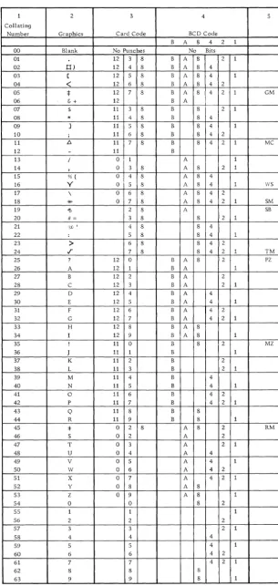
1 2 3 4 5 Collating
Number Graohics Card Code BCD Code
B A 8 4 2 1
00 Blank No Punches No Bits
01 12 3 8 B A 8 2 1
02 tl) 12 4 8 B A 8 4
03 [ 12 5 8 B A 8 4 1
04
<
12 6 8 B A 8 4 205
*
12 7 8 B A 8 4 2 1 GM06 (; + 12 B A
07 $ 11 3 8 B 8 2 1
08
*
11 4 8 B 8 409 ] 11 5 8 B 8 4 1
10 ; 11 6 8 B 8 4 2
11 fj. 11 7 8 B 8 4 2 1 MC
12 - 11 B
13 / 0
I 1 A 1
14 , 0 3 8 A 8 2 1
15 % ( o
I
4 8 A 8 416 Y o 5 8 A 8 4 1 WS
17 \ 0 6 8 A 8 4 2
18 -ttt- 0 7 8 A 8 4 2 1 SM
19 15 2 8 A 5B
20 #~ 3 8 8 2 1
21 ,0) I 4 8 8 4
22 : 5 8 8 4 1
23 > 6 8 8 4 2
24 .r 7 8 8 4 2 1 TM
25 ? 12 0 B A 8 2 PZ
26 A 12 1 B A 1
27 B 12 2 B A 2
28 C 12 3 B A 2 1
29 D 12 4 B A 4
30 E 12 5 B A 4 1
31 F 12 6 B A 4 2
32 G 12 7 B A 4 2 1
33 H 12 8 B A 8
34 I 12 9 B A 8 1
35 ! 11 0 B 8 2 MZ
36 J 11 1 B 1
37 K 11 2 B 2
38 L 11 3 B 2 1
39 M 11 4 B 4
40 N 11 5 B 4 1
41 0 11 6 B 4 2
42 P 11 7 B 4 2 1
43 Q 11 8 B 8
44 R 11 9 B 8 1
4S :j: 0 2 8 A 8 2 RM
46 S 0 2 A 2
47 T 0 3 A 2 1
48 U 0 4 A 4
49 V 0 5 A 4 1
50 W 0 6 A 4 2
51 X 0 7 A 4 2 1
52 y 0 8 A 8
53 Z 0 9 A 8 1
54 0 0 8 2
55 1 1 1
56 2 2 2
57 3 3 2 1
58 4 4 4
59 5 5 4 1
60 6 6 4 2
61 7 7 4 2 1
62 8 8 8
63 9 9 8 1
Figure 3. Standard BCD Interchange Code
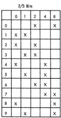
[image:11.618.69.375.55.699.2]2/5 Bits
0 1 2 4 8
0 X X
1 X X
2 X X
3 X X
4 X X
5 X X
6 X X
7 X X
8 X X
9 X X
Figure 4. Two-Out-of-Five Code
QUI-BINARY CODE
1410 arithmetic units use qui-binary representation of numeric characters (Figure 5). The qui-binary code offers more advantages than BCD in numeric addition and carry generation. During operations involving the arithmetic unit, data in BCD form is translated into qui-binary, treated arithmetically, and retranslated into BCD. To translate from BCD to qui-binary, the 1 bit be-comes a binary 1 (Bl). The 2, 4 and 8 bits become a qui-nary 0, 2, 4, 6, or 8 (QO, Q2, Q4, Q6, or Q8). For example a 9 in qui-binary is a Bl and a Q8; an 8 is a BO and Q8; a 1 is a Bl and QO; etc.
Packaging and Component Parts
All units of the IBM 1410 System use the standard mod-ular system (SMS) concept of design. Electronic cir-cuitry is completely solid-state, using transistors and
Card Code BCD True Add Complement Add
0 8.2 QOBO Q8 B1
QO B1 Q8 BO
2 2 Q2 BO Q6 B1
3 1.2 Q2 B1 Q6BO
4 4 Q4 BO Q4 B1
5 1.4 Q4 B1 Q4BO
6 2.4 Q6 BO Q2 B1
7 1.2.4 Q6 B1 Q2 BO
8 8 Q8 BO QO B1
9 1.8 Q8 B1 QOBO
Figure 5. Qui-Binary Code
12
m~gnetic cores. Maximum usage is made of saturating
drift transistor registor lOgiC (SDTRL) circuits. These cir-cuits are used because of their reliability, high speed, and low cost. All circuitry is in the form of plugable cards containing transistors and their associated circuits.
Storage Principles
Magnetic core storage is used in the IBM 1411 Central Processing Unit. Characters are stored in the core-storage unit in binary-coded decimal (BCD) form. This requires seven bit locations, or core planes (C B A 8 4, 2, 1) for each character position. An eighth
c~r~
plane provides for the storage of word marks (see "Word Mark").ADDRESSING
Core-storage units are available with 10,000, 20,000, 40,000, 60,000, or 80,000 character positions. The ar-rays are arranged so that each character position can be individually addressed.
Each core-storage address is five character positions. Valid addresses for a machine with 10,000 characters of storage are 00000 to 09999. Valid addresses for a ma-chine with 20,000 characters of storage are 00000 to 19999. Valid addresses for a maximum-capacity ma-chine with 80,000 characters of storage are 00000 to 79999.
An attempt to use an invalid address results in an error. The numeric portion of the five-character address must consist only of valid numbers from
°
to 9. An at-tempt to use speCial character or blank codes in ad-dresses results in an error-stop (address validity). The zone bits over the tens and hundreds positions are re-served for index tags as explained in "Indexing." The units-, thousands-, and ten-thousands-positions must contain a no-zone indication, or an error stop results.Core storage addressing is as follows:
1. To address an instruction in core storage, specify the location of the high-order character (operation code).
2. Data fields to be moved from one core storage area to another, or fields to be operated on arithmeti-cally, are addressed by specifying the location of the low-order character of the field. Characters are moved or operated on arithmetically in a low- to high-order sequence.
3. For all data movements that originate or termi-nate outside the core storage, and for record moves within core storage, the data is addressed by specifying the location of the high-order character. Therefore, data addresses of all input-output operations, including the file, specify the location of the high-order character. On an 1-0 operation, characters are moved from high to
[image:12.623.35.138.58.257.2]NOTE: Low order and high order refer to the posi-tions of an instruction word or a data word as they would appear on a printed form or as a field in a card. Do not confuse these terms with the storage addresses which are numbered left to right, low to high in rela-tion to a data word or an instrucrela-tion word.
DATA WORD
A data word is one complete unit of information that is comparable to a field in a card, such as an account number.
VARIABLE WORD LENGTH
A data word may be a single character, or a group of characters. Words are not limited to any fixed number of character positions in the storage unit.
WORD MARK
To define the length of a word, a word mark is stored as a single bit in the eighth core plane of storage in the high-order position of that word. This word-mark core-plane is in all storage positions. Thus, the high-order position of a word can be placed at any storage address. SCANNING
The core-storage unit can read out only one character at a time. A whole word must be read out character by character. The order in which these characters are read out is determined by the machine. For example, when two fields are added together, the units position of the fields must be read out first to determine the signs of the fields. Information read out to an output machine is read out high order to low order.
The treatment of these words, character by character, is known as scanning. Reverse scanning is the reading out from high order to low order, as in reading out to I-O machines. Forward scanning is the reading out of the low-order position first.
Stored Programming
The IBM 14lO System is controlled entirely by stored programming. A sequence or program routine of oper-ations is stored or loaded in the core-storage unit before the system: processes data. The processing unit then proceeds, step by step, through the stored-program routine, analyzing each instruction and performing the function called for before proceeding to the next in-struction.
Just as program routines or jobs in the machines using control panels can be changed by changing con-trol panels, a stored-program routine can be changed by loading a new routine into the storage unit via an input machine.
INSTRUCTION WORD
The instructions in core storage consist of a variable number of alphameric characters that combine to make up an instruction word. Valid instruction words vary in length from 1 to 12 characters, depending on the amount of information that the operation requires.
Valid instruction formats are:
o
o
do
XXXdo
AAAAAo
AAAAAdo
XXXBBBBBdo
AAAAA BBBBBo
AAAAA BBBBB do
signifies the Single-character operation code; AAAAA is the five-character address of the A field. BBBBB is the five-character address of the B field. xxx is the three character I-O unit and control field, and d is the opera-tion modifier.The instruction words are arranged sequentially in core storage. Subsequent instructions are located in higher-numbered storage positions. Each instruction word must have a word mark with its operation code. Any other word marks will result in a machine-stop when the word reads out. A word mark must also be in the location immediately to the right of the low-order character of the instruction word. Usually this is the operation code for the next instruction.
The address of an instruction is the location of its operation code.· No operation code has two valid lengths that differ by only one character. Instruction-length checking insures that the instruction Instruction-length as read out of storage is one of the valid lengths for the particular operation code. The add op code, for exam-ple, has three valid lengths: 1,6, or 11 characters.
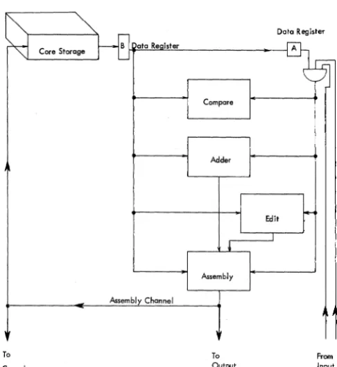
Control
The central processing unit (cpu) is made up of four major areas: a storage unit, an address unit, an opera-tional unit, and a control unit.
1. The storage unit is the center of all data flow in the 1410. Information reads into storage from the as-sembly channel and reads out through a B data regis-ter to the B channel. A five-position address is fed to the storage unit to control the position of storage to be used.
2. The address unit stores and modifies the five-posi-tion addresses that locate the posifive-posi-tion of storage to be used.
3. The operational unit contains all the units neces-sary to edit, compare, move or add data.
4. The control unit contains registers, cycle controls, and a clock that are necessary to perform the various functions of the CPU.
The operation of the IBM 1410 System is controlled
by the program routine stored in the core-storage unit. The completion of each program step requires two phases: instruction (I) phase and execute (E) phase.
INSTRUCTION PHASE
I phase is the first portion of the program step that is required to read the instruction word out of storage. The instruction word is made up of addresses, op code, op modifier, and control characters for 1-0 operations. As the characters read out during I phase, they are stored in registers in the control or address units. A storage cycle is required to read each character out onto the B channel. Because the length of the instruc-tion words is variable, the number of cycles in I phase
is variable.
I phase is further divided into I cycles. To identify which character of the instruction word is reading out of storage during an I cycle, an I ring counts the char-acters or cycles. The I ring consists of 13 triggers la-belled I ring op, and I ring 1 through I ring 12 (Fig-ure 6).
As the first I cycle of I phase is taken, the I ring is set to I ring op time to identify this character as the op code. The I ring then advances to I ring I-time to iden-tify the next character that reads out as either a modi-fier, or the ten-thousands position of an address, de-pending on the op code character that has already been read out and recognized.
An example of I phase is a data move instruction
word which can consist of the op code, followed by an A field and B field address and a d modifier character:
y
D AAAAA BBBBB d
At I ring op time, the op code reads out of the stor-age unit and is set into the op register in the control
unit. The op register is decoded to identify the next five
characters as the A field address.
I rings 1 through 5 gate the characters into the proper positions of an address register, located in the address unit, called the A address register.
I rings 6 through 10 gate the next five characters to the B address register in the address unit. The
charac-ter read out at I ring 11 time is the d modifier. It is
I-cy I-cy lOp I 1
y D
Op
Reg A
-I-cy I 2
A
I-cy I-cy I 3 I 4
A A
AAR
Figure 6. Instruction Phase
14
I-cy I-cy I-cy I-cy I-cy I-cy I 5 I 6 I 7 I 8 I 9 I 10
A B B B B B
BAR
I-cy
I 11
d
stored in the op-modifier (op mod) register in the con-trol unit. During I ring 12 time, the next character is read out to insure that a word mark is located in the next position of storage.
EXECUTE PHASE
At the completion of I phase, the machine is ready to perform the actual operation. This portion of the pro-gram step is the execute phase (E phase). The length and complexity of E phase depends on the type of op code. E phase can consist of A, B, C, D, E, or F cycles, with storage either forward- or reverse-scanned. Each cycle length varies from 4.5 to 7.5 (4.0-6.67) microsec-onds. At the completion of E phase, the machine nor-mally returns to I phase to initiate the next instruction.
Data Flow
The center of data How in the IBM 1411 Central
Proc-essing Unit is the core-storage unit that receives data
from the IBM 1405 Disk Storage Unit, the IBM 1415
Console, or the IBM 1414 Input-Output Synchronizer
(Figures 7 and 8). When processing is complete, the data can be sent to the 1405, 1415, or 1414.
The 14141-0 Synchronizer controls the various input-output units that are used in conjunction with the 1410 System. The 1414 includes the integrated synchronizer, print storage, and tape adapter units.
The integrated synchronizer is an input-output con-trol unit that contains up to eight 80-character mag-netic-core storage units. These units provide independ-ent buffering for all associated 1-0 units. A data transfer
between the CPU and the card read punch or paper tape
reader takes place through the integrated synchronizer.
Processing time is saved because the CPU does not have
to wait for a mechanical unit to pick up speed, etc. The print storage unit contains a 132-position core-storage unit that is an intermediate core-storage device
be-tween the CPU and the IBM 1403 Printer. Included in
the print area is the circuitry necessary to control the carriage for forms handling.
The tape adapter units provide a control system for the various tape units that may be used with the 1410 System.
I-cy I 12
v
0
Op Mod.
1405
1415
..
1411 DiskConsole , ~
Central Processing Unit Storage
Units
1414 Input/Output Synchronizer
- - - -- - -- - - -T- - - -T
-, I
I I Tape
Integrated I Print I
I I Adapter
Synchronizer I Storage , ,
Units
I ,
I I I
____ 1 ___
~~1402-2
Optional 1011 729
Card Paper 1403
Read Serial Tape Printer 7330
Punch Devices Reader Tape Units
Figure 7. Data Flow
Figure 8. CPU Data Flow
OP REG SET CK
ADDRESS EXIT CHANNEL
ASSEMBLY CHANNEL
Tic COMPARE
17" 15.01
16.12"01 16.13.01 ADDER
ASSEMBLY 15.50.01
Tic
Ull> m
r(") (")I » II> ",;0 n
:I:
»
z ~
VC 18.11.01
18.13.01
CONSOLE
42.10.01
- t = : I / O S Y N C FCU'1
TAU'I
I/O SYNC
- FCUll
TAU'I SENSE SW
~
CONSOLE~_ 156001-08
15.56.08-09
15
15.70.04
The IBM 1411 Central Processing Unit is the hub of all
1410 System operations. Four frames form the integral units of the basic 1411. Frame A contains power sup-plies, circuit breakers, and relays necessary for power control and distribution throughout the system. Frame B contains the magnetic core storage unit. Instructions that define operations to be performed and the data to be operated upon can be stored in this unit indefinitely.
Frame B also contains the SMS transistor cards that
make up the address unit circuitry. The address unit stores the five-position addresses that locate positions in core storage to be used.
Frame C contains logic clock circuitry that generates timing pulses for the 1411 and also contains the cycle control unit. The adder and assembly circuits are also
located in frame C. Internal data How in the 1411 is
controlled partially by the assembly unit. Operation de-code circuits in frame D analyze each instruction word to determine the what, where, when, and how of any operation. Also in frame D are the compare and edit control units. Input-output circuits necessary for the
How of data into and out of the 1411 are located in both
C and D frames.
Control Unit
The lOgiC clock generates timed impulses that are used to form gates that control all functional units of the 1411.
Logic Clock
Various 1410 System operations require different length storage cycles. These cycles range from six to ten pulses; the number of pulses depend on the type of operation being performed. The pulses are called lOgic
gates A through K. The lOgic clock circuit uses a
free-running crystal-controlled oscillator and a ten-trigger ring to develop the number of logic gate pulses re-quired (Figure 9).
The oscillator drives a binary input trigger called the clock pulse trigger. The outputs of the clock pulse trig-ger are called "first clock pulse" (lcp) and "second clock pulse" (2cp). The clock is normally stopped with the stop latch that, by collector pullover, clamps the clock pulse trigger at lcp. The lOgic gate A trigger is also on. When the stop latch is reset, the clock pulse trigger is . advanced by the oscillator. At the end of 2cp, the ring
1411 Functional Units
is advanced from logic gate A (LGA) to lOgiC gate B
(LGB). Since clock pulses are .375 (.333) microseconds
long, the ring advances every .750 (.666) microseconds (Figure 10).
Cycle length is defined by controlling the point at which the ring stops advancing and returns to its start-ing position. Type of cycle and type of operation
con-trol cycle length by conditioning the "stop at F, H,
J,
orK line." This line combines with the corresponding
logic gate pulse to bring up "last logic gate (LLG)." LLG
sets the logic gate Z latch that gates the ring back to
LGA. To stop the clock at the end of a cycle, the stop
latch is set on by the 2cp of the last logic gate. The stop latch combines with lcp to clamp the clock pulse
trig-ger at lcp, LGA (Figure 11).
UNOVERLAP OPERATION
All 1-0 commands (except F or K) can be executed one
of two ways: unoverlapped or overlapped. An
unover-lapped command causes the CPU to take E cycles
(chan-nel2) or F cycles (channel 2), as required, to read in or
read out each 1-0 character. Because the CPU reads in or
reads out characters at a faster rate than any 1-0
ma-chine, the CPU must wait between each E or F cycle
until the 1-0 device sends, or is able to receive, another
character.
During E phase of an unoverlapped 1-0 instruction,
"compute disable cycle" comes up to stop the clOck by
preventing (by collector pullover) the LGA trigger from
coming on. The clock pulse trigger continues to
ad-vance. When an 1-0 cycle is needed, "E, or F cycle
re-quired" overrides "compute disable cycle" to allow the ring to advance through the cycle. Logic gate Z that
gates LGA on is reset by LGA. As long as "compute
dis-able cycle" prevents LGA from setting, LGZ remains on
until another 1-0 cycle is required (Figure 12).
OVERLAP OPERATION
An overlapped 1-0 instruction allows the CPU to use the
time between E or F cycles for compute cycles.
Six triggers, added to the clock circuits, form a
lOgiC gate extension ring. These are triggers LGR through
LGW. When an overlapped 1-0 cycle is taken, the
exten-sion ring is used instead of the normal logic-clock ring (Figure 13).
Logic gate Z gates on both LGA and LGR. When "E or
F cycle required" is up in an overlapped operation, it
Stop Latch 12.15.04
Osc.
11.10.01
Clock Pulse Trigger 11.10.02
Compute ~isable
Hold LGA "Off"
Not E or F Cy Req Unovlp A >-_:":':':::"';=~'=':'':'''-_-I-_ _ _ _ _ _ ...J
11.10.10
Figure 9. Logic Clock
'Oscillator
'Oscillator Delayed Stop Latch 1st Clock
2nd Clock Logic Gate On and Off Advance
Logic Gate A Trigger ---"l ... ________________
r-L
Logic Gate 8 Trigger
-I7sl
(.666)r
Logic Gate C Trigger Logic Gate 0 Trigger Logic Gate E Trigger Log ie Gate F Trigger logic Gale G Trigger Logic Gate H Trigger Logic Gate J Trigger Logic Gate K Trigger Next to Last Logic Gate Stop On K
Last Logic Gate Logic Gate Z
• INPuTS TO CLOCK PULSE TRIGGER
Figure 10. Logic Clock Pulses and Gates
18
Stop at J
Dis 10 Routine 2nd Scan D-C
Alter No Scan
Stora e Scan Sto Ke Latch
Figure 11. 1410 CPU Clock Control
Osci Ilator 1.33 mc (1.5)
11.10.01
Not E Ch in Process Not F Ch in Process 1st Clock Pulse
Code I Rin 9
B Ch WM Bit LGD
Master Error
12.15.04
Computer Reset
Master Error
Computer Reset and Clock Start Console Strobe Start Ke Pulse
Clock Pulse Trigger
11.10.02 Stop Latch
1st Clock Pulse 2nd Clock Pulse
lst C P
2nd C P
LG A
LG B
LG C
LG 0
LG E
LG F
LG G Stop At G Last LG
LGZ
Campute Disable Cycle
E or F Cycle Req (Unovlp)
7}/$$/$////#//////////& -...IL
---1 L
Figure 12. Compute Disable Cycle
conditions "compute disable cycle" to hold LGA off and
allows LGR to set. When 1-0 cycles are not needed, LGR
is held off and LGA is allowed to set for another
com-pute cycle.
Figure 14 shows a sampling of pulses developed from the logic clock and a timing chart that illustrates I phase being stopped to take an overlap E cycle.
NaE or F Cy Req (Unovlp)
Clock Pulse Trigger 11.10.02
Hold A "Off"
Cycle Control
Cycle latches A through F, I, or W identify storage
cycles. Type of cycle and operation determine cycle length. The cycle latch is on from lOgiC gate B to lOgic
gate B. Cycle latches control different areas of the CPU;
the I cycle latch identifies the character that is being
read out of storage as part of an instruction word. I
cycle also gates the modified address into the IAR.
Each cycle latch has a control latch that is usually set at the next-to-Iast logic gate of the previous cycle. For
example, at the end of the I cycle at I ring op-time, the
I cycle ctrl latch is set to keep the I cycle latch on for
the next storage cycle.
The A cycle latch usually identifies the character that is being read out of storage as an A field character. The B cycle usually identifies the character as a B field character. E and F cycles are used for input-output operations. C, D, and X cycles are used for special operations.
Four more control latches assist in identifying char-acters as they are read out of storage. They are: units,
body, extension, and MQ.
For example, an add operation is performed where the contents of the A field are added, a digit at a time, units position first, to the contents of the B field. The first cycle after I phase is an A cycle during which the units position of the A field is set into the A data regis-ter. The next cycle is a B cycle during which the units position of the B field is read out onto the B channel. The units latch is set for the first A and B cycles to
Unoverlap
E or F Cy Req o Compute Disable Cy A '>--+--+---' 12.12.60
Figure 13. Overlap
20
E or F Cy Req Overlap
13.60.04
I Hold R
Stap At F _ _ --'-_...I
~
~;;~~~~==~~~~~~~~P~U~IS~e~S~D~e~v~elo~p~e~d~F~r~om~T~h~e~L~O~QliC~C~IO~Ck~~~~~~~~:;~~;===::::::::::::==
SIGNAL NAME ~T~E:~:~ LOGICI CloCk Pulse IIC2:J04H 11.10.02 1·2.1·2·j ·2'1·2·1 ·2·1·2·1 '2·1 ·2·1·2·1·:!.1 .2: 1·2·1·2·1·2'1 ·2'1·2·1·2·1 ·2·1·2.
2 r-;L:O:9i::-C-;;R~in:::9:-;Ad:;:V:--t-tll-;C~2:~KO~~±[I;;-I.~10:;.0:;5tt-l-::=-= ....
:=.-=
....
=--:-=
.... :...:..
...
:=.~.... ::. ....
..:....::::.:....
...
..::~....
::.I""I...:...::..:..:: .... ::..:..:...:: .... :..:...:..I""I::;~ .... ::....:..:.: .... :....:.. .... ::;...:..:.: ... ::... .... ~:.:.:..: ... ::..:....--.:...:....:-.:....:...:...:...:...:...:-. 3 r~L:OO~i~C~G~o~te~s~--r*:1~II;C2~~~0*:t.1;;-1.:10~D~2~A~.~8~.~c~· B~.~.~E~.~F~.~R~.~S~.=T~.C~~.~.~v~.CW~.~A~.~B-.~C~.=D~.~E~.c;FJ.~AL-.-.~~~~~~..:...:.~ 4 r-~N~L~L~G~ot:e~s---r*~:II~C~I:~H~I~;~r.1~2.~12~.3~1~~~~~.~ ~~~ .. ~.~.~.~~~~.~ ~~~.~.~.~~~~~.~ ~~~.~.~.~~~~~..:...:.~~~ 5 r7L~L~G---r*~711~cjl~~0~2~fl~2.~12~.3~1t-~--~.~.-.-~~=-_.----L.-.~~L--.---L.=.~~L-~.~~-.:....:...:.-.:...:...:...:....~~ 6 r7L~G;Z~---r*~~II~C~2:~F~~r.I~I.I~0~D~6t-~---.-.-.-~~=.-. _ _ _ _ _ .-.~~c=l-.---.~.~~c=~.~~-.:....:...:...:...:...:...:....~~ 7 r~E~a~r'Y~La;'S;tr.G:at:e---r*;i~"~C~2:~Kcr7~7~"~I.'~0~.0~6t-~~~~.7.~~~~.~.~~~~~.~ ~~~.-.---.~ ~c=~.~.~~-.:..~..:...:...:...:....~~ 8 r~A~n~y7L~OS=t~G~a~te~--r*:i~II~C~2:tK~I1R;r.I~LI~0.~0~6t-~~~~~.-~~=--.---.~.=~~-.--____ ~.~.=~:L~.~~-':"":""':'-':"":""':''':''''':''''':'~ 9 t-·~I7.ns~tr=u~ct~io=n~R~0~Gt~-r~7.II~C2~:~F04~4~(I~I.I~Q~07~It:--,=-·---L~---~·L-·l-~--.----~~---~.:...:...:....~...:....:-.:....:...:.~ 10 r7L~G~Sp=e=Ci~a~1 ~A~~-r-i7.II~C2~:tH~17~Cr.I~13~0~D~21r.:__,:-.~~~~~~~~~~~~-.-~~==L_.---.--~ __ --.~.:...:.~~..:...:.~..:...:.~ II LG Early B IIC2:HI7D 11.30.01 r--'I' . ,... .12
~~B~to~LL~G~====~~~II~C~2:~DI~3~K~I~1.3~Q~.~~~~~~~~~================~~~::::::~~====================
13 LG Eorly F * IIC2:J2IH 11.30.01 . ,..., . . ,..., .14 r---~~----
__
~~~:~4r~~r---~~i---L==L---15
*
Pulses that vary with cycle I~ngth.16 r---~T-~~~f---_+---~~~~~~~~~
17 An· Ovarlap· E Cycle .
18
r---~_f--~_f----+_----~~~~---19
~~I~C~y~CI~e~======~=tI~IC~I~~~2~2~~I~~12~.04~.~=r~~~~:=:=:=~==============~:=:=:=:=:=:=:=~================
20 RO IAR IICI :CI2HI4.71.341...., . . ..., . . ,... .21
~~E:C~Y~C~le~======~=l~IID~3~1~~~~12t.~12~.6~6~.~.=.==============~~~~~~~~~==========~==~===============
22 ~~R~0~EA~R~ ______ ~-f~II~C~I~=0~2~(14~~~I.~3~5r-·_·_· __________ · i _ ~ _ _ L-. ______________________________________________ _
23 Set STAR 1182 :<l26~ 14.17.16 M' . . ,., . . . 1""1 . . ,.., •
24 r-~R-eo~d-C~O~II~----~--+I~IC~2~iD~16~H~II~.1~0.~32'1-L--,~·---.~ ~~-.---.~ ~~-.---.~
~~-.---25
!~E~C~Y~C~le~R!e~q~Ui~re~d~~~I~ID~3~~~1~8Q~12~.1~2~D~2~.~ ~
..~-~-~-~.~---~~-~~~~~~~~~~~~~~~~~~~~~~~~~~~
26 Compute Disoble IID3P02r 12.12.60 .r-.---27 E Ch Ovlp in Proc 1103 :8081 13.60.0<1
Figure 14. Logic Clock Pulse Timings
identify the characters as units-position characters be-cause that is where the signs of the fields are located.
The body latch is set after the units position is set and stays on until the end of the A field. The extension latch identifies the remaining B field characters that have no corresponding A field characters (Figure 15).
E B U
X 0 N
T D I
Y T
S
+
A-Field 0 2 9 0
+
B-Field 0 2 9 8 7 0
-I-0 2 2 6 0
Figure 15. Control Latches
The MQ latch is used in multiplication and division to
identify a character as a position of the multiplier or
quotient. The MQ latch is also used in edit and zero
suppress op codes.
Address Unit
The address unit, which stores and modifies the five-position addresses that locate the five-position of storage to be used, contains eight address registers. One of these,
the storage address register (STAR) is used as an output
of the address unit that is fed to the core-storage unit.
The STAR is read into from anyone of the seven other
address registers (labeled A through F, and I), or from the address generator (used for indexing). The address unit also contains an address modifier that is used to
add one or subtract one from the address in STAR to
obtain the address of the next position of storage (Fig-ure 8).
Address Registers
An address register (AR) is a temporary storage device
that reads in or out the five-digit addresses that are re-quired to locate information in core storage. Characters are stored in the address registers in the two-out-of-five code.
Each address register position has five latches corre-sponding to theO, 1, 2, 4 and 8 bits used in the 2/5 code.
The functions of these address registers are:
1. Instruction Address Register (IAR). This is used to locate and scan instruction words.
2. A Address Register (AAR). This locates the data word to be used as the A field of an instruction.
3. B Address Register (BAR). This locates the data word to be used as the B field of an instruction. The A
~nd B field addresses are read into the AAR and BAR,
re-spectively, when an instruction word is read out of storage.
4. C Address Register (CAR). This usually contains
the same address as the AAR at the beginning of the
execute phase (E phase).
5. D Address Register (DAR). This usually contains
the same address as the BAR at the beginning of the E
phase. The CAR and DAR are used in multiply, divide,
recomplement, table search, and other operations. 6. E Address Register and F Address Register. These two registers contain the storage locations for
charac-ters going to or coming from I-b machines during
over-lapped. operations. Overlapping is an optional feature and is discussed in "Overlap."
READ INTO ADDRESS REGISTERS
(lAB, AAR, BAR, CAR, DAR, EAR, AND FAR)
Circuits for all address registers are very similar. For
example, the 8 bit latch in the hundreds position (HP 8B)
of the BAR is shown in Figure 16.
Before BAR is read into, the BAR reset line resets all
latches off. If the "address channel 8 bit" line is up
(active), the top leg of the AND circuits of all AR 8B
latches is up. "Set AR HP" is up on the second leg of all
BAR Gate Out HP 8 B AR Bus HP 8 B
Not.: Only on IAR
Figure 16. Address Register Latch (14.11.03)
22
hundred position latches of all address registers. "Set
BAR" is up to complete the coincidence necessary to set
this latch.
READ OUT OF ADDRESS REGISTERS
(IAR, AAR, BAR, CAR, DAR, EAR, AND FAR)
When the CPU requires the next character of the B field
word, "read out BAR (RO BAR)" gates the output of every
latch in the BAR to the AR bus. All positions of the BAR
read out in parallel. "Set STAR" sets the storage address
register with the bits received on the AR bus, which
causes the addressed character to be read out of storage.
STORAGE ADDRESS REGISTER
Since every CPU cycle is a storage cycle, STAR is set in
parallel from the address bus at the beginning of each cycle. The storage address register has no "reset" line as have the other seven address registers; it is reset by a program reset operation only. Using the previous
ex-ample, the STAR HP 8B latch is turned on or off
depend-ing on the status of the bit lines from the address bus.
An active bit line turns on its corresponding STAR latch;
an inactive bit line turns off its corresponding STAR
latch (if that latch was on).
SUMMARY OF ADDRESS REGISTERS
1. All 1410 address registers store addresses in the two-out-of-five code.
2. All address registers except STAR read in serially
via the address channel starting with the ten-thousands position when an instruction word is read out of
stor-age. (The IAR is also set in a parallel from STAR. See
"Instruction Read-Out."
3. All address registers read out in parallel.
4. STAR is used as an output of the address unit. The
output of anyone of the other address registers is gated
in parallel via the address bus to STAR at the beginning
of each storage cycle.
Address Modification
The address in the address registers (AR) locate, in
storage, the first character of the next word to be read out. This character is the units position of the field if the word is to be forward-scanned, or the high-order
position of the field if the word is to be reverse-scanned.
For every character read out of storage, the address of
that character must first be read into STAR. To develop
address in STAR to develop the address of the next char-acter is called address modification.
The address modifier must be able to:
1. Subtract one from the address when forward-scanning.
2. Add one to the address when reverse-scanning. 3. Recognize when it is subtracting one from a zero
in order to borrow one from the next higher posi-tion.
4. Recognize when it is adding one to a nine in order to carry one into the next higher position.
OPERATION
Address modification must be completed during the shortest storage cycle; 4.5 (4.0) microseconds (Figure 17). During storage cycles longer than 4.5 (4.0) micro-seconds, address modification is still completed from logiC gates B through F.
During a cycle where the A address register (AAR) is used to read out a data word, the address in the AAR is set into STAR (Figure 18) on the second clock pulse of logic gate A. The AAR resets on the first clock pulse of logic gate B, while the units position of STAR is gated to the address modifier.
Yes
No Scan Ctr! -Mod by Zero 1st Scan Ctrl - Mod by Minus One 2nd Sccn etrl - Mod by Plus One 3rd Scan Ctrl - Mod by Minus One
LGB SetUP
LGC SetTP
LGDSetHP
LGE SetThP
LGF SetTThP
Operation is Complete After LGF
Figure 17. Address Modify Operation
The address modifier controls are set to modify by minus one by first scan control. The CPU contains four scan-control latches. The first or third scan latches are on when scanning storage from units to the high-order positions. The second scan latch is on when scanning from high- to low-order positions. The no scan latch is on when the address of the character is not to be "hanged.
Modify by minus one and the 0 from STAR combine to bring up 8 bit and 1 bit lines which are gated into the units position of the AAR on the second clock pulse of logic gate B.
When the address modifier subtracts 1 from 0, it keeps the mod by minus one latch on to borrow one from the next position. The 2 in the tens position of STAR is gated to the address modifier at logic gate C and combines with modify by minus one to send a 1 to the tens position of the AAR.
The modifier controls are set to modify by zero, which passes the rest of the address unaltered through the modifier.
CIRCUIT OBJECTIVES
1. Reset the address register, depending on the type of cycle. For example, A cycle reads the modified result into the AAR, B cycle reads the address into the BAR; I cycle reads into the IAR.
2. Set modifier controls and after modifying the units position, controls are set to mod by zero except when minus one and a combination of 2 and 8 bits (borrow one) or plus one and a combination of 1 and 8 bits (carry). (See Figure 19.)
3. Gate STAR to address modifier. 4. Combine mod controls and character. 5. Gate result to address register.
NOTE: Objectives 2 through 5 are repeated for all five positions.
Figure 20 shows address modify timings involved during an instruction read-out operation.
ADDRESS MODIFY CIRCUIT DESCRIPTION
Refer to Figure 18 when following this description.
1. Reset the address register.
SIGNAL CONTROL
Reset AAR A Cycle Ctrl 2. Set modifier controls. Addr Mod Set to 1st Scan Ctrl
Minus One
Set Mod by Minus One Addr Mod Set to Minus One
Mod by Minus One Set Mod by Minus One 3. Gate STAR to address modifier.
LOGIC
14.71.20
14.71.41 14.30.08 14.30.08
Mem AR UP 2B to AddrMod
Mem AR 2B Latch LGB 14.17.02
...
..t:....
....
""
«
1;
V)
To Storage Unit ,--_ _ ~A _ _ _ ~
r
\
LG B
LG C
LG 0
LG E
LG F
Set STAR
2 cp LG A
Modify By - 1
Reset AAR 1st Clock Pulse L.G .B.
Set AAR 2 cp LG B thru F
...
...
... ...
Address Channel ..t: .... :r:....
::::>t><
""
""
""
f---
Storage Cycle----j« « «
-
«-
1;..
1;I
AI
BI
C"
V) V) V) V)1st Clock Pulse 2nd Clock Pulse
SetSTAR ~
R~MAAR
----IlL-Gate U.P. S TAR To Addr.
--.r-L
Set U.P. AAR- - . f L
I
0GateT.P.STARToAddr. ~
Set T.P. AAR
IL
I
EI
FI
AI
Figure 18. Address Modification of ARR
24
-1 2.8 Line
Not Stora Scan I Cycle Control
2nd Scan Ctrl EC Ctrl FC Ctrl Star Scan Routi ne
CE Mode,Starage Scan Switch +1
Mod
Not - 1 2.8 Line Not +1 1.8 Line Cor D C Ctrl
Scan Switch Zero +1 2.8 Line
Figure 19. Address Modify Latches
2nd CP
2nd CP
SElt Mod Ctrl Latch lstCP
Reset Addr Mod Ctrl Latches
+1 1.8 Line 2nd CP
Addr Mod Set to +1 Logic Gate A
2nd CP Nat +1 1.8 Line Set Mod Ctrl Latch
Reset Addr Mod 1 Cantrol Latches
2nd CP
2nd CP
lstCP Reset Addr Mod Control Latc hes
Pro Reset
Lo ic Gate Z
2nd CP
Lo i c Gate A+R
Mod -1
Reset Address Mod Latc h
Reset Address Mod Latch
Mod
By 0
Ctrl Latch
Reset Address Mod Latch
Reset Addr Mod Ctrl Latch 14.71.40
Reset Addr Mod Control Latches
Mod -1 Latch
14.30.08
Mod +1 Latch
Mod By
0
Latch
'"
o o <t o
i A B
A
03998 C 0
op
0 03999
A B-.L.~.L~
I
o 04000
,
A
5 04009
II
. r+-, .
. r-+--,
-r:h.
l...,·
I ,..., .
! ' n ' " , .I·
n ' . n '. 'n':
. r - 1 ' . ,--, . ''--'' ' r ! '
.
,...,
. . ''-' . 'J'"'1 .. r-1 . 'r=1
. r ! . , r - 1 ' 1 . r I '
. r-1 .
. 'r-! '
·ri·. . o· -0' -0' ·4· ·0 1 • ·1· ·0· ·0· .4 . . o! , .0 . . 1 . . 0 . . 4 . .o.!
,
, r---t. .:
~ __________ -4 __ ~~-4 ____ ~+-_'~"'~_' ______ ~ __ '~~-L' ________ ~_'~n-L_' ---+-~~---'-·r!,·
' M ' ' I " " \ ' n ' n '
l
'.1""t' . l"'1' n 1""\
r---~~--~~~+_+_---.~ M_'~ _______ '~ M_' ri ________ .~ ~._+-__ ---'~'
f--_~ _ _ +_-+--1--~~+__:__----. ....J.,..;_+'-' - - - - ' ..J...ri+: - ' - - - - ' ... rI+-· --- - - :
4
I - 0 " : ,0· r
r , !
I -0' " 'I
I---"---+-+--'--+--+i±"t~:!---.---. -r+,-+-.-.---.-M-'I!-' - - , ---r-n-"'---,-,
"'-"---«"r±i
Figure 20. Address Modify Timing
4. Combine mod controls and characters.
Minus One 2 and 8 Line
Addr Mod IB and 8B Addr Ch IB"
AAR-UPlB Addr Ch8B" AAR-UP8B
Mem AR 2B 8B and Mod by Minus One Minus One 2 and 8 Line Addr Mod 1 and 8B Addr Mod 1 and 8B
5. Gate result to address register.
Set AAR Set ARU Pas
A Cycle LG-B, C,
D,E&F
LGB-2nd CP
6. Set modify controls.
14.30.06 14.30.06 14.45.02 14.45.05
14.71.10 14.71.01
Set Mo