© 2017, IRJET | Impact Factor value: 5.181 | ISO 9001:2008 Certified Journal | Page 86
An Area Efficient Mixed Decimation MDF Architecture for Radix
Parallel FFT
Reshma K J
1, Prof. Ebin M Manuel
21
M-Tech, Dept. of ECE Engineering, Government Engineering College, Idukki, Kerala, India
2
Professor, Dept. of ECE Engineering, Government Engineering College, Idukki, Kerala, India
---***---Abstract
- Fast Fourier Transform (FFT) has got manyapplications in the field of digital signal processing. In this project, an area efficient Mixed decimation Multipath Delay
Feedback ( DF) methodology have been presented for the
radix FFT computation. The DF architecture can be
employed by using the principle of folding transformation. Thereby the idle period of arithmetic units in Multipath Delay Feedback (MDF) architecture can be mobilized. This is done by the integration of Decimation-In-Time (DIT) operations into the Decimation-In-Frequency (DIF) operated computing units.
The DF architecture system design was modified by using
Han Carlson adder which is efficient in area and fast in
operation. Besides, the DF system is compared with
proposed DF system using Han Carlson adder both
theoretically and experimentally. From the obtained expressions and statistics, it can be concluded that the proposed system can be used as an area efficient system since it achieves improved efficiency in the consumption of arithmetic resources. The hardware simulation is done in Xilinx Virtex-6 Field-Programmable Gate Array (FPGA), using the programming software ISE 14.2 Vivado Design Suite.
Key Words: Fast Fourier Transform (FFT), Multipath
Delay Feedback (MDF), Decimation-In-Time (DIT), Decimation-In-Frequency (DIF), Pipelined architecture.
1. INTRODUCTION
Fast Fourier Transform (FFT) is an efficient algorithm for Discrete Fourier Transform (DFT) computation. Therefore, an efficient implementation of FFT has attracted much consideration and various schemes have been put forward by the hardware designers to achieve reasonable tradeoffs between area and performance. When compared to other hardware structures, pipelined architectures [1]-[6] have a characteristic advantage over other efficient hardware structures in providing high throughputs. Single path Delay Commutator (SDC) structure [1] is one of the most conventional approaches to perform the pipelined FFT computation in the Serial Input Serial Output (SISO) scenario. Single path Delay Feedback (SDF) architecture [1] is proposed in order to decrease the memory banks in SDC pipelines. SDF architecture is composed of many feedback connections in the circuits. These architectures can be used with any algorithm such as radix-2, radix-4, and especially
radix- algorithm in order to execute the DFT operation. The radix- pipeline is equipped with simpler butterfly units when compared to radix-4 approach while making a better utilization of complex multipliers than the typical radix-2 scheme.
From the perspective of hardware design, radix-algorithm acts as an effective alternative to the conventional computation methods. Certainly, the extension of communication service has encouraged a dramatic rise of throughput requirements. The demand for high throughput can be achieved by using another upgraded structures [2]. These structures can be used to calculate the FFT when several samples of the same sequence are received in parallel. So Multipath Delay Commutator (MDC) [3] and Multipath Delay Feedback (MDF) [4] are proposed to improve the throughput rate. MDC and MDF work as the upgrade of SDC and SDF respectively.
In general, multiple interconnected SDF paths are joined together to form MDF structure. Each SDF path is used for managing one of the parallel input streams. This design contributes to efficient utilization of memory resources but it has got only 50 % utilization of adders and provides only less throughput. By contrast, the hardware efficiency of arithmetic units (AUs) can be improved by using the MDC approach. But for either regrouping the samples or folding the streams, additional memories have to be consumed. This will again additionally leads to an increase of computing delay. The feedback structures such as SDF and MDF design afford possible solutions to make a balance between the consumption of hardware resources and the reachable performance [4].
As we move forward the discussion, the hardware resources can be further divided into two categories: arithmetic resources and memory resources. Arithmetic resources are associated with logical or arithmetic operations and memory resources are responsible for caching samples. The MDF scheme [4] has been a great success in a variety of applications due to the outstanding performance in the efficient use of memory resources. Beneath the triumph, the underutilization of arithmetic resources is still an important problem for feedback design and has not been determined satisfactorily.
© 2017, IRJET | Impact Factor value: 5.181 | ISO 9001:2008 Certified Journal | Page 87
The objective of this project is to design a new areaefficient mixed decimation MDF architecture which can achieve improved efficiency in utilization of arithmetic resources while maintaining the advantages of feedback structures. The theory of folding transformation is employed to derive the proposed scheme namely, the mixed decimation Multi path Delay Feedback ( DF) architecture. The integration of Decimation-In-Time (DIT) operations into the Decimation-In-Frequency (DIF) operated building blocks can activate the idle period of arithmetic units in MDF architectures. Thus significant decrease in the consumption of arithmetic resources can be achieved by DF architecture.
2. MIXED DECIMATION MDF SYSTEM
DF architecture is derived from the theory of folding transformation. This will activates the idle period of arithmetic units in MDF architecture. The operations in SDF pipeline are rescheduled to reverse the underutilization of arithmetic modules which is accomplished by integrating the DIT operations into the DIF operated computing units. So there by better efficiency in the consumption of arithmetic resources [4].
[image:2.595.312.551.84.363.2]2.1 SDF DIF Scheme Using Folding Transformation
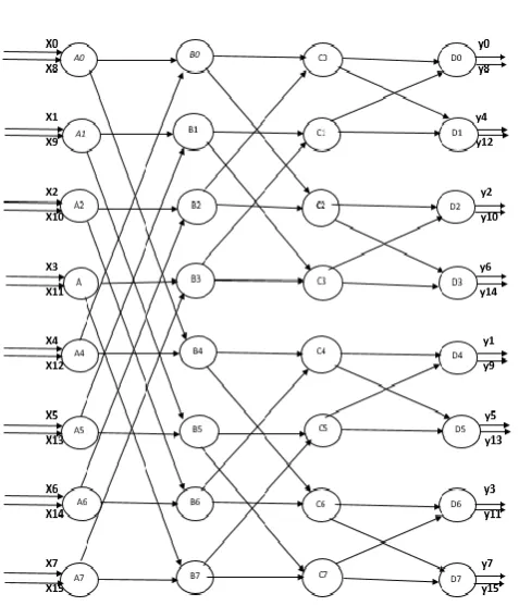
The folding transformation offers a methodical procedure to derive many FFT architectures. In folding transformation, several algorithm operations are time multiplexed on a single computing device [5]. The algorithm can be presented using a data flow graph shown in Fig 1, where the nodes represent computations and the directed edges represent data paths. The data flow graph consists of four stages and eight operations are executed within each stage. When , i = 0, …, 15 arrives in serial, multiple operations in each stage can be time multiplexed to a single computing unit without any collisions and the control circuits are determined systematically by folding transformation. In this way, the FFT Flow graph shown in Fig 1 can be converted into a pipelined form as shown in Fig 2 , where operations A0, …, A7, B0, …, B7,C0, …, C7 and D0, …, D7 are performed in the computing unit , , and respectively [4]. The multiple operations included in a computing module are arranged by folding sets. A folding set is an ordered set of operations executed by the same computing unit. Each folding set contains many operations and some of which may be generally called as null operations, Ф.Fig -1: Data flow graph of 16 Point R 2^2 DIF FFT
Fig -2: Data flow graph converted into a pipelined version through folding transformation
The folding set corresponding to , , and can be written as :
= {Ф Ф Ф Ф Ф Ф Ф Ф A0 A1 A2 A3 A4 A5 A6 A7}
= {Ф Ф Ф Ф B0 B1 B2 B3 Ф Ф Ф Ф B4 B5 B6 B7}
= {Ф Ф C0 C1 Ф Ф C2 C3 Ф Ф C4 C5 Ф Ф C6 C7 }
= {Ф D0 Ф D1 Ф D2 Ф D3 Ф D4 Ф D5 Ф D6 Ф D7}
[image:2.595.315.559.405.472.2]© 2017, IRJET | Impact Factor value: 5.181 | ISO 9001:2008 Certified Journal | Page 88
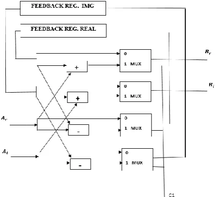
Fig -3: 16 Point R 2^2 SDF DIF FFT structureEach stage in radix- SDF FFT [6] contains of butterfly I, butterfly II, complex multipliers with twiddle factors. Butterfly I operate on the input data, butterfly II operate on the output data from butterfly I, then multiplied with twiddle factors to get the result of the current stage. Shift registers or Random Access Memory (RAM) are used to store the output data from butterfly elements. Only one complex multiplier is used, since, input data sequence follows a single output path. Butterfly 1 structure [6] is shown in Fig 4. The input for this butterfly comes from the previous component which is the twiddle factor multiplier. The output data from butterfly 1 goes to the next stage which is usually the butterfly II. The control signal C1 has two options. That is either C1=0 or C1=1. When C1=0, multiplexers direct the input data to the feedback registers until they get filled. The other option is C1=1, the multiplexers select the output of the adders and subtracters.
Fig -4: Butterfly 1 structure
Butterfly 2 structure is shown in Fig 3. The butterfly 2 structure [6] is same as that of butterfly 1. But in additional, there is a swap-mux provided for –j multiplication. The multiplication by –j contains swapping between real part and imaginary part and sign inversion. Swap-MUX is efficiently used for swapping real and imaginary part and the
[image:3.595.37.280.77.196.2]sign inversion is handled by switching between the adding and the subtracting operations by mean of swap-MUX. The control signals C1 and C2 will be one when there is a need for multiplication by –j .
Fig -5: Butterfly 2 structure
2.2 SDF DIT Scheme Using Folding Transformation
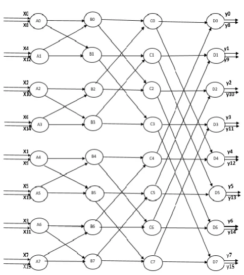
The DIT algorithm can also be represented using a data flow graph shown in Fig 6. Similar processes as in DIF can be applied to analyze DIT algorithm. As shown in the Fig 6, the flow graph contain four stages and eight operations are performed within each stage. When , i = 0, . . . ,15 arrives in serial, multiple operations in each stage can be time multiplexed to a single computing unit without any collisions and the control circuits are determined systematically by folding transformation [5]. In this way, the FFT Flow graph shown in Fig 6 can be converted into a pipelined form through folding transformation as shown in Fig 7, where operations A0, . . . , A7, B0, . . . , B7,C0, . . . ,C7 and D0,……D7 are executed in the computing unit , , and respectively. The folding set corresponding to , ,
and can be written as :
={Ф A0 Ф A1 Ф A2 Ф A3 Ф A4 Ф A5 Ф A6 Ф A7}
={Ф Ф B0 B1 Ф Ф B2 B3 Ф Ф B4 B5 Ф Ф B6 B7 }
= {Ф Ф Ф Ф C0 C1 C2 C3 Ф Ф Ф Ф C4 C5 C6 C7}
[image:3.595.313.540.163.374.2] [image:3.595.52.273.448.650.2]© 2017, IRJET | Impact Factor value: 5.181 | ISO 9001:2008 Certified Journal | Page 89
Fig -6: Data flow graph of 16 Point R 2^2 DIT FFTFig -7: Data flow graph converted into a pipelined version through folding transformation
When obtaining the folding sets associated with , , and , the supporting circuits used to fulfill the time multiplexing of computing units can be obtained through folding transformation [5]. By using register minimization method implementation system can be further optimized which eventually generates the SDF hardware structure which is shown in Fig 8. There by hardware efficiency can be enhanced. The DIT SDF hardware structure is exactly the reverse of DIF hardware scheme.
Fig -8: 16 Point R 2^2 SDF DIT FFT structure
The folding sets conveys the fact that , whether the designers adopt the DIF approach or DIT scheme to construct the SDF circuit, the existence of null operations in folding sets will always reduce the efficiency of arithmetic components. This will lead to an approximate 50% utilization of complex adders merely. To address this issue, we rearrange the operations in SDF pipelines to activate the idle intervals of computing units [4].From the SDF DIF and SDF DIT hardware structures we can clearly understand that both DIF and DIT approach uses same hardware resources .But only difference is that DIT is the reverse of DIF scheme. So by integrating the DIT operations into DIF operated computing units, the standby time of arithmetic modules in feedback architectures can be eliminated. The integration of DIF and DIT pipelined processor to fully utilize the computing units is shown in Fig 9.
Fig -9: Integration of DIF and DIT pipelined processor
[image:4.595.310.556.295.542.2] [image:4.595.40.275.399.467.2] [image:4.595.41.283.645.740.2]© 2017, IRJET | Impact Factor value: 5.181 | ISO 9001:2008 Certified Journal | Page 90
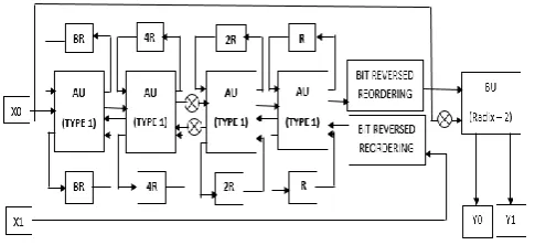
Fig -10: Type 1 structureFinal system DF design can be constructed by using this Type 1 structure. Fig 12 shows the system design of two parallel DF design for 32 point FFT. During 32 point DFT processing, and execute DIF and DIT scheme respectively. represent first 16 input samples and represent next 16 input samples. In addition, as input samples required to be rearranged as bit reversal before participating in DIT computation. The DIT output samples are multiplied by necessary twiddle factors for 32 point FFT computation. Finally parallel streams are connected to simple radix 2 butterfly unit to get 32 output samples for FFT [4].
Fig -11: System design of two parallel
DF architecture for 32 Point FFT3. PROPOSED
DF SYSTEM
In any of FFT architectures, Butterfly unit is the important block to calculate data addition and substraction.An adder is the main building block of butterfly element. The key requirement of adder is that the adder should be fast in operation and efficient in terms of chip area. So the
performance of butterfly unit can be further enhanced by using high speed and an area efficient adder [7].
3.1 DF Design by Using Han Carlson Adder
The simplest method of doing binary addition is to connect
the carry-out from the previous bit to the carry-in of the next bit. Each bit takes carry-in as one of the inputs and gives sum and carry-out as output bit and therefore named as ripple carry adder. This type of adders is made by cascading 1 bit full adders. But ripple carry adder has high propagation delay. So DF system designed by using ripple carry adder have only small performance [7]. [image:5.595.319.540.424.603.2]The
DF system design is modified by using high speed and an area efficient Han Carlson adder. Han Carlson adder is a parallel prefix tree [8]. Parallel prefix adders are high performance adders. Han Carlson adder is shown in Fig 13 and it uses only even bits for performing carry-merge operations. Generate and propagate signals of odd bits are transferred down the prefix tree. The true carry bits are produced by the recombination of generate and propagate signals with even bit carry signals. So by using high speed and area efficient Han Carlson adder, system design can give better performance.Fig -12: 16 Bit Han Carlson adder
4. RESULTS
[image:5.595.39.282.501.612.2]© 2017, IRJET | Impact Factor value: 5.181 | ISO 9001:2008 Certified Journal | Page 91
4.1
DF System
[image:6.595.35.293.190.372.2]Fig 14 shows the simulation result of two parallel 32 point R 2^2 DF FFT. a1 and a2 represent two 16 point parallel DIF and DIT input samples respectively. t_r and t_img are the 32 point output samples for given input samples and clock signal,clk.
Fig -13: Simulation result of two parallel 32 point R 2^2 DF FFT
4.2
Proposed
DF System
[image:6.595.314.557.484.634.2]DF architecture is modified by using high speed and an area efficient Han Carlson adder. So the Proposed DF System is found to be area efficient. Fig 15 shows the simulation result of proposed two parallel 32 point R 2^2 DF FFT. The simulation result obtained is same for both system design and proposed scheme.
Fig -14: Simulation result of two parallel 32 point R 2^2 DF FFT
4.3
Performance Analysis
The performance analysis was done on both system design
and proposed DF system design. The occupation of slices is evaluated for comparing hardware efficiency. Table 1 shows the design summary of system design and proposedDF system for 32 point FFT.
Table -1: Device utilization summary of system design and proposed DF system
Structures Slice
LUTs Slice registers LUT FF pairs Total DF
Architecture 1561 7722 1082 10365
Proposed DF Architecture
1527 7717 1078 10322
From the device utilization summary, we can understand that when DF system was modified by using area efficient Han Carlson adder, there is decrease in the utilization of slice registers, slice LUTS and no of fully used LUT FF pairs than the DF system designed with ripple carry adder. There by we obtained a new area efficient hardware for DF architecture. Chart 1 shows the graphical representation of above obtained test results in table 1.
Chart -1: Device utilization summary of system design and proposed DF system
5. CONCLUSIONS
[image:6.595.36.292.530.710.2]© 2017, IRJET | Impact Factor value: 5.181 | ISO 9001:2008 Certified Journal | Page 92
was designed by using Verilog HDL in Xilinx ISE 14.2 DesignSuite. The performance of adders can again be enhanced by using high speed adder. The DF architecture system was then modified by using high speed and an area efficient Han Carlson adder. Performance of both system design and proposed system was analyzed. Area and delay are taken as the parameters for performance analysis. Hardware is obtained to be efficient for proposed system by 0.4%.
ACKNOWLEDGEMENT
I would like to thank my project guide Prof. Ebin M Manuel for his constant support and timely advice throughout my work. He consistently steered me in the right direction especially during my research and writing which helped me to complete my work successfully.
REFERENCES
[1] A. Cortes, I. Velez, and J. F. Sevillano, “Radix r^k FFTs: Matrical representation and SDC/SDF pipeline implementation, ” IEEE Trans. Signal Process., vol. 57, no. 7, pp. 2824–2839, Jul. 2009.
[2] C. Cheng and K. K. Parhi, “High-throughput VLSI architecture for FFT computation, ” IEEE Trans. Circuits Syst. II, Exp. Briefs, vol. 54, no. 10, pp. 863–867, Oct. 2007.
[3] M. Garrido, J. Grajal, M. A. Sanchez, and O. Gustafsson, “Pipelined radix-2^k feedforward FFT architectures, ” IEEE Trans. Very Large Scale Integr. (VLSI) Syst., vol. 21, no. 1, pp. 23–32, Jan. 2013.
[4] Jian Wang, Chunlin Xiong, Kangli Zhang and Jibo Wei, “A mixed decimation MDF architecture for radix 2^k parallel FFT, ” IEEE Trans.on very large scale integration, vol. 24, no. 1, pp. 414–426, Jan 2016.
[5] M. Ayinala, M. Brown, and K. K. Parhi, “Pipelined parallel FFT architectures via folding transformation, ” IEEE Trans. Very Large Scale Integr. (VLSI) Syst., vol. 20, no. 6, pp. 1068– 1081, Jun. 2012.
[6] Yazan Samir Algnabi, Rozita Teymourzadeh, Masuri Othman, Md Shabiul Islam” FPGA Implementation of Pipeline Multiplier-Less Radix 2^2 DIF SDF Butterfly for Fast Fourier Transform Structure”, MicroEngineering VLSI Design Department, June 2012
[7] Mallapu Santhosh Kumar1 and K.Dhanunjaya (Ph.d), “Comparison of Various 32-Bit Parallel Prefix Adders, “International Journal for Research in Applied Science & Engineering Technology (IJRASET), ISSN: 2321-9653, Volume 3, Issue VI, Jun. 2015.