N A N O E X P R E S S
Open Access
Effects of Al Doping on the Properties of
ZnO Thin Films Deposited by Atomic Layer
Deposition
Chen-Hui Zhai
1, Rong-Jun Zhang
1*, Xin Chen
2*, Yu-Xiang Zheng
1, Song-You Wang
1, Juan Liu
3, Ning Dai
2and Liang-Yao Chen
1Abstract
The tuning of structural, optical, and electrical properties of Al-doped ZnO films deposited by atomic layer deposition technique is reported in this work. With the increasing Al doping level, the evolution from (002) to (100) diffraction peaks indicates the change in growth mode of ZnO films. Spectroscopic ellipsometry has been applied to study the thickness, optical constants, and band gap of AZO films. Due to the increasing carrier concentration after Al doping, a blue shift of band gap and absorption edge can be observed, which can be interpreted by Burstein-Moss effect. The carrier concentration and resistivity are found to vary significantly among different doping concentration, and the optimum value is also discussed. The modulations and improvements of properties are important for Al-doped ZnO films to apply as transparent conductor in various applications.
Keywords:Al-doped ZnO thin films, Atomic layer deposition, Optical properties, Spectroscopic ellipsometry, Electrical properties
Background
A transparent conductive oxide (TCO) has received con-siderable attentions and been widely used in electronic and optoelectronic devices [1], such as solar cells [2], liquid crystal [3], and high-definition displays [4], due to their low resistivity and high transmittance. There are various TCO materials, including In, Sb, Zn, Cd, Sn metal oxides, and their composite oxides. Among them, indium tin oxide (ITO) film is the most widely used TCO material [5]. However, the scarce and toxic nature of indium and instability of ITO are the main obstacles for its further development, which arouses the interests of researchers to explore alternative TCO materials for ITO. As a candidate for TCO, ZnO films doped with trivalent metal cations have attracted considerable atten-tions [6–9]. Thereinto, Al-doped ZnO (AZO) film is one of the most promising candidates [10], since it has many
advantages, such as low cost, abundant resource, non-toxicity, and good stability in hydrogen plasma. Impor-tantly, the optical and electrical behaviors of AZO films can be improved or modified by controlling their doping level [11], which is critical to achieving functionalization and tunability of TCO-based devices. Therefore, it is useful to investigate the correlation between the proper-ties of AZO films and the concentration of Al doping.
Various methods have been used to prepare AZO films, including atomic layer deposition (ALD) [12, 13], chemical vapor deposition (CVD) [14, 15], magnetron sputtering [16, 17], and pulsed laser deposition (PLD) [18]. Compar-ing to other techniques, ALD is an excellent deposition technique based on self-limiting surface chemical reactions that can be used to prepare highly uniform and smooth films while their thickness can be precisely controlled.
Various properties of ALD-based AZO films have been reported by many research groups [19–22]. Among these properties, optical properties are generally studied and analyzed based on transmission and photolumines-cence spectra [21, 22]. However, there are few reports on the properties evaluated by spectroscopic ellipsome-try (SE) analysis [17]. SE known for its precision and
* Correspondence:[email protected];[email protected] 1Department of Optical Science and Engineering, Ministry of Education, Key
Laboratory of Micro and Nano Photonic Structures, Fudan University, 220 Handan Road, Shanghai 200433, China
2National Laboratory for Infrared Physics, Shanghai Institute of Technical
Physics, Chinese Academy of Sciences, Shanghai 200083, China Full list of author information is available at the end of the article
non-destructiveness is a useful tool for the optical characterization of nanostructures [23, 24]. Thickness, optical constants, and band gap energy information can be determined accurately by using SE. With increasing the Al doping level, the modulation of the optical pro-perties provides references to the change of electrical characteristics.
In this work, we investigated the structural, optical, and electrical properties of AZO thin films deposited by ALD technique with a wide range of doping levels. The effects of concentration of Al doping on properties of AZO thin films were discussed in detail. The thickness, optical constants, and band gap of AZO samples were calculated by fitting ellipsometry data in a broadband spectral region. The modulated transmittance of AZO thin films was shown by transmission spectrum mea-surement. The blue shift of band gap and absorption edge were observed and discussed in light of Burstein-Moss effect. The electrical properties of the films were measured by using a Hall effect measurement system. The optimum concentration of Al for resistivity was studied with the structural and optical properties keep-ing excellent as well.
Methods
Both pure ZnO and Al-doped ZnO thin films were prepared on the Si and quartz substrates through a custom-made ALD reactor. The deposition procedure was at a temperature of 150 °C and a working pressure of 80 Pa. Diethylzinc [DEZ; Zn(C2H5)2] and
trimethyla-luminum [TMA; Al(CH3)3] were used as the precursors
for Zn and Al, respectively, and deionized water (H2O)
was used as the oxidant reactant. High purity nitrogen (N2) with a gas flow rate of 50 sccm (standard cubic
cen-timeters per minute) was used as the carrier to deliver precursors into the chamber and purging gas to take the needless products away from the chamber. During the de-position process, the DEZ and H2O were alternatively
in-troduced into the chamber to grow the ZnO films through DEZ-H2O cycles (DEZ/exposure/N2/H2
O/expo-sure/N2), with pulse times of 0.03/3/15/0.03/5/15 s. For
Al-doping into the ZnO films, TMA-H2O cycles of Al2O3
were introduced with the same process as the DEZ-H2O.
The ZnO and Al2O3 monolayers grow through their
surface reactions [25]. The structure diagram of the inves-tigated AZO film is shown in Fig. 1. The film deposition consists of several super cycles while one super cycle consists of one monolayer of Al2O3andn monolayers of
ZnO. Different Al content of AZO films was obtained by varying the number of ZnO monolayers during one super cycle. Hence, various numbers of DEZ-H2O cycles and
one TMA-H2O cycle were repeatedly carried out for film
depositions, as the cycle ratio given in Table 1. Same number of ZnO monolayers (N2) was adopted for each
sample to fix the thickness of the main body of the films which could avoid the thickness effects on the properties of samples. According to N2 and the cycle ratio of DEZ-H2O and TMA-H2O, the number of super cycle or
Al2O3 monolayers (N1) and the total numbers of cycles
(N,N= N1 + N2) is also determined.
The chemical compositions and chemical bond states of the thin films were characterized using X-ray photo-electron spectroscopy (XPS). XPS analysis was carried out through a scientific spectrometer (Axis Ultra DLD) with an Al KR X-ray source (1486.6 eV). The phase and crystallinity of samples were measured by X-ray diffrac-tion (XRD; Bruker D8 ADVANCE) with Cu Kαradiation (λ= 1.5418 Å). The images of atomic force microscopy (AFM) of samples were obtained by using a Bruker Dimension Icon microscope VT-1000 System operated in tapping mode. The spectroscopic ellipsometry measure-ment was carried out by a vertical variable-angle SE (V-VASE; J.A. Woollam Co., Inc.) in the wavelength range of 200–1000 nm with a spectral resolution of 5 nm. The incident angle was selected as 65, 70, and 75° to insure the reliability of fitting results. Optical transmission spectra were measured with a double beam UV-VIS-NIR spectro-photometer (Shimadzu UV-3600) in the wavelength range of 250–1000 nm. And the electrical properties of the films were measured by using thevan der Pauw method with a Hall effect measurement system (Ecopia HMS3000). All these measurements were carried out at room temperature.
[image:2.595.305.540.89.222.2]Fig. 1The structure diagram of the AZO films
Table 1Deposition parameters for samples, Al composition of AZO films via XPS, and film thicknesses fitted by SE
Samples DEZ-H2O/TMA-H2O
cycle ratio N
1 N2 N at. %Al Thicknesses (nm)
ZnO – – 200 200 – 41.2
AZO 50:1 50:1 4 200 204 3.7 % 41.7
AZO 20:1 20:1 10 200 210 4.9 % 44.3
AZO 10:1 10:1 20 200 220 7.1 % 46.8
[image:2.595.305.541.639.732.2]Results and Discussion
Composition and Structure Analysis
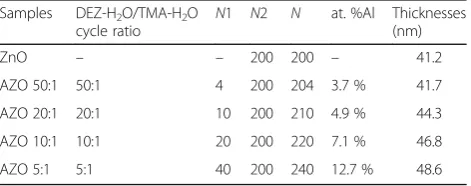
To verify the concentration of Al doping, the XPS mea-surement was carried out on Al-doped ZnO films. Figure 2 reveals the XPS spectra of the AZO films after calibration with carbon peak. In Fig. 2a, the high symmetry energy peak of Zn 2p3/2 is located at 1021.3 ± 0.1 eV, which is
approximately equal to the value of Zn in bulk ZnO [26].
It indicates that Zn in AZO films exists in the oxidized states. From Fig. 2b, the main peak located at 530.0 ± 0.1 eV is assigned to lattice oxygen bonded as O2−ions in the ZnO matrix [27]. Here, carbon composition has been removed from those spectra, so no peak of carbon com-position can be observed in Fig. 2b. As for Fig. 2c, the energy peaks of Al 2p exhibit a symmetry feature, and is located at around 73.5 ± 0.1 eV which is corresponding to the characteristic peak of Al2O3[28]. The growth of peak
intensity indicates the increase of Al concentration in the films. The concentration of Al is calculated from the ratio of Zn, Al, and O atoms, as shown in Table 1. With varying the cycle ratio of DEZ-H2O and TMA-H2O from 50:1 to
5:1, the Al concentration increases from 3.7 to 12.7 %. The X-ray diffraction patterns of samples grown on Si are shown in Fig. 3. To obtain clearer phenomenon of crystallinity, the samples were annealed at 400 °C in N2
atmosphere for 1 h. The crystalline structure of the films exhibits a hexagonal wurtzite structure with growth directions of ZnO (100) or (002). No clear peaks of Al2O3 manifests the deposited Al2O3 is amorphous
under the growth conditions in this work. The crystal-line state and crystal orientation of these films are found to change with the increasing doping concentration of Al3+. The pure ZnO film shows a preferred growth with ZnO (002) direction, and the peak position locates at about 34.5°. However, the (002) peak disappears and new ZnO (100) peak becomes dominant after Al doping. The evolution of ZnO peaks demonstrates that Al-doping affects the growth mode of ZnO films, which is similar to the results reported by Banerjee et al. [29]. With further increasing Al doping, no peak is observed for AZO 5:1 sample, which indicates the AZO film at 12.7 at.% Al is amorphous. Since the Al2O3 layer by ALD is
amor-phous in our growth conditions, the Al2O3 doping layers
Fig. 2XPS spectra of AZO films grown on Si substrates: (a) Zn 2p
[image:3.595.58.292.189.709.2] [image:3.595.307.539.532.712.2]destroy the crystal quality of the AZO 5:1 films, which causes the disappearance of its (100) peak. From Fig. 3, it can also be observed that the ZnO (100) peak shifts to a larger diffraction angle with the increasing Al3+ content. Here, the Al3+ions (ion radius 0.53 Å) is smaller than Zn2+ ions (ion radius 0.74 Å), so the increasing Al concentration will reduce the lattice constant of samples by substitutions of Zn2+ions with Al3+[30].
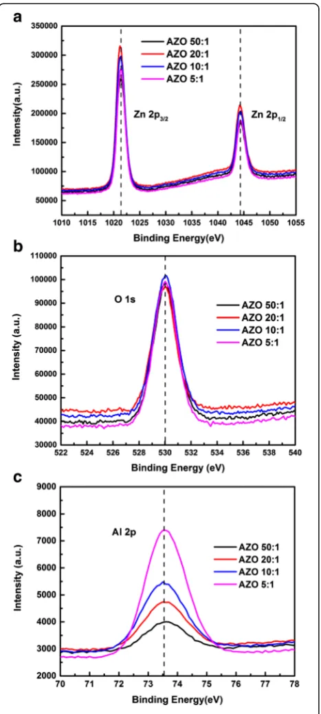
The surface morphologies of the samples grown on Si substrates are analyzed by using the AFM method with a scanning area of 5 × 5μm2. The 3D AFM images of the samples are shown in Fig. 4. All the films show good uniformity over the whole scanning area. The hill-shaped features with average lateral dimensions 50–100 nm can be observed on the surface of samples. The root-mean-square roughness (Rq) of each samples calculated from
AFM data is less than 1.00 nm, as given under their AFM images, respectively. It is clear that all samples present smooth surface with inessential surface roughness.
Therefore, the surface scattering is weak enough for SE analysis, which makes the analysis more reliable [31].
Optical Properties of Samples
Spectroscopic ellipsometry is generally applied for the investigation of the thickness, optical properties of samples, which is based on measuring the change in the polarization state of a linearly polarized light reflected from the sample surface. In order to get more accurate information, Si is selected as the substrate to provide enough reflected light in SE measurement. For SE analysis, an optical model of our samples is firstly con-structed, which consists of a semi-infinite Si substrate/ pure ZnO or AZO film/air ambient structure. No rough-ness layer is introduced, due to the smooth surface of samples revealed by AFM measurements. The obtained ellipsometry spectra (ΨandΔat range of 200–1000 nm) of the films are fitted by using the Forouhi-Bloomer dispersion model (Additional file 1)[32]. This dispersion
[image:4.595.59.538.332.722.2]model is widely used to describe the optical properties in the spectral region which is dominated by inter-band transitions and contains the information of the band gap [32]. The thickness, optical constants, and band gap of the films are evaluated in a fitting procedure by minim-izing the root-mean-square error (RMSE) which defined as follows [33]:
RMSE¼
ffiffiffiffiffiffiffiffiffiffiffiffiffiffiffiffiffiffiffiffiffiffiffiffiffiffiffiffiffiffiffiffiffiffiffiffiffiffiffiffiffiffiffiffiffiffiffiffiffiffiffiffiffiffiffiffiffiffiffiffiffiffiffiffiffiffiffiffiffiffiffiffiffiffiffiffiffiffiffiffiffiffiffiffiffiffiffiffiffiffiffiffi
1 2x−y−1
X
i¼1
x Ψcal
i −Ψexpi
2
þ Δcal
i −Δexpi
2
h i
s
ð1Þ
Here,xis the number of data points in the spectrums, yis the number of variable parameters in the model, and “exp” and “cal” represent the experimental and the calculated data, respectively.
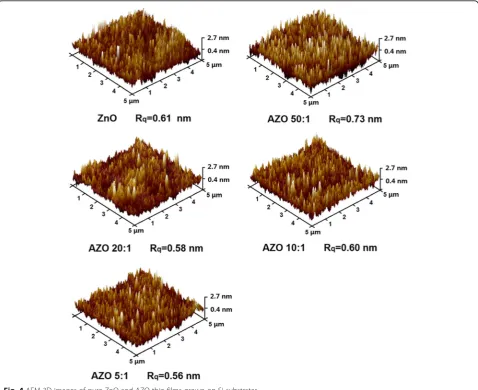
The fitted thickness of samples is shown in Table 1. With the increasing concentration of Al, the thickness of the film displays a growing trend due to the increased total numbers of cycles. Figure 5 illustrates the refractive index n and extinction coefficient k of the films with various doping levels at the wavelength range of 200– 1000 nm. The calculated optical constants of the pure ZnO films obtained by ALD are in good agreement with our previous work [34]. Due to the Al doping is not deep enough, optical constants of AZO 50:1 is very close to pure ZnO. Figure 5a demonstrates the refractive indexn of the films with various doping levels. Obviously, the refractive index of films decreases gradually with doping level increasing, since Al impurity can act as effective n-type donors to generate free carriers. The doping of Al2O3 increases the free carrier concentration in films,
which results in the decrease of the refractive index of the films [35]. So, the refractive index can be modulated by Al doping level. Figure 5b describes the extinction coefficient k of the films with various doping levels. It can be seen that thekof all films is close to zero infinitely in the wave-length range of 400–1000 nm, which indicates that the
films are nearly transparent in this wavelength region. Besides, a blue shift of the absorption edge can be observed with the increasing doping level.
In order to better understand the blue shift of absorp-tion edge, Tauc method is used to calculate the band gap of the sample by using formulas as follows [35]:
αhν
ð Þ2¼A E−E
g
ð2Þ
α¼4πλk ð3Þ
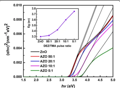
whereAis a constant,Egis the optical band gap energy, α is the optical absorption coefficient which can be calculated from extinction coefficient (k) and wavelength of SE results. In order to simplify the calculation, Tauc extrapolation is utilized to obtain the band gap energy of samples. As shown in Fig. 6, we made a plot of (αhν)2 versus the photon energy. The optical band gap can be determined by the linear fitting. Through extrapolation, the point value of fitted line andxaxis isEg, as revealed
in the inset figure of Fig. 6. The band gap of the ZnO film is 3.3 eV, which agrees well with the ideal band gap of pure ZnO. And the Eg displays a growing trend with
the increasing concentration of Al. The tendency is simi-lar to that of other elements doped ZnO and In2O3:Sn
films (TCO materials) [36]. It can be interpreted by the Burstein-Moss effect [36, 37]. ZnO is an type semicon-ductor material with direct transition, and its Fermi level will enter into the conduction band when it is heavily doped. The state below Fermi level is occupied by elec-trons. The absorption transition process of light can only exist between the valence band and the vicinity to Fermi level. It results the optical band gap of films moves to the high energy region. Moreover, the Burstein-Moss effect is related to the carrier density. Extrinsic Al3+are substituted for Zn2+in the AZO films, so the spare elec-trons from Al3+ can increase the concentration of free carriers in films, resulting in the growth of optical band
[image:5.595.59.541.562.713.2]gap of the films. It can be described by the equation as follows [18]:
Eg ¼Eg0þΔEBMg ¼Eg0þ h 2
8me
3 π
2=3 n2e=3 ð4Þ
whereEg0,ΔEgBM,ne,h, andme*are the intrinsic forbidden
band width, band gap increment caused by Burstein-Moss effect, electron carrier density, Planck’s constant, and the effective electron mass in the conduction band, respect-ively. In addition, the ideal band gap of pure ZnO is 3.3 eV and that of Al2O3is 8.7 eV [29]. So, with the increasing Al
doping level, the band gaps of films are increased.
Figure 7 illustrates the transmittance spectra of sam-ples with various doping levels. The absorption edge of the samples can be found in the range from 300 to 400 nm. Blue shift of absorption edge is observed clearly with rising Al doping level, which is consistent to the
results of SE analysis shown in Fig. 5b. This blue shift could be attributed to the rising of band gap energy resulting from Burstein-Moss effect. With the increasing Al doping level, the optical band gap of films is growing, which causes the absorption edge shift to short wave-length region. Moreover, it is clear that the optical trans-mittance of the films was slightly enhanced with the growing Al content, and the transmittance in the visible region is still higher than 85 %. The transmittance value is close to that of other common TCO films [38], which is important for the applications in the field of solar cell.
Electrical Properties of Samples
Transparent conductor is one of the most common applications of AZO films. The electrical property of AZO films is also an important factor for its performance in devices. So, carrier concentration and resistivity of the films are assessed by using a Hall effect measurement system. In order to avoid the spatial resistivity distribution, the films are deposited on quart substrates, and their test results are revealed in Fig. 8. In the case of pure ZnO film, the carrier concentration and the resistivity were 1.77 × 1019 cm−3 and 5.98 × 10⁻¹Ωcm, respectively. As Al incorporated into ZnO films, the carrier concentra-tion of AZO films at first increases rapidly and then reaches to the maximum value of 4.41 × 1020 cm−3 for AZO 20:1 film. After that, the carrier concentration of AZO films was abruptly reduced. As for the resistivity, it displays an opposite tendency, and the lowest value is 1.28 × 10⁻²Ωcm also for AZO 20:1 film. The carrier concentration and resistivity of our AZO films are similar to other results of ALD-based AZO samples [20, 29, 39]. But it is slight different from those of AZO films deposited by the other methods, which use the bulk incorporation of dopants. By contrast, Al atoms in ALD-based AZO films
Fig. 6Evaluated optical band gap of samples grown on Si substrates
Fig. 7Transmittance spectra of samples grown on quartz substrates with various doping levels
[image:6.595.58.290.88.259.2] [image:6.595.58.290.522.703.2] [image:6.595.305.539.531.702.2]would be more easily to cluster and form stoichiometric Al2O3 (insulator) [20]. Therefore, the carrier
concentra-tion of ALD-based AZO samples is a little lower, while the resistivity is a little higher.
From Fig. 8, the resistivity of pure ZnO is the highest due to its low carrier concentration. After Al doping, extrinsic Al3+substitutes into host Zn2+sites and provides an extra electron, which improves the carrier concentra-tion. So, the resistivity decreases in the beginning. With the improving doping level, the increase of Al2O3 (insulator)
concentration leads to the rise of resistivity. In addition, the lowest resistivity is 1.28 × 10⁻²Ωcm for AZO 20:1 film, as shown in Fig. 8. So, the optimum Al concentration is 4.9 at.%, AZO 20:1, which is deposited by controlling a number of super cycles consistent with a DEZ/H2O:TMA/
H2O cycle ratio of 20:1, as mentioned in the experimental
section. Furthermore, AZ0 20:1 films possessed not only optimum carrier concentration and resistivity but also excellent optical transmission in solar cell absorption wave-length range. It is crucial for AZO films to be applied as transparent conductor.
Conclusions
We have investigated the structural, optical, and electrical properties of ALD-based AZO films with doping concen-trations ranging from 3.7 to 12.7 at.% for applications as transparent conductor materials. The inessential surface roughness within 1.00 nm shows the high morphological quality of the films deposited by ALD technology. The diffraction peak shifts from ZnO (002) to ZnO (100) with increasing Al content indicate that Al doping can change the growth mode of ZnO films. SE analysis has been adopted to reveal the thickness, optical constants, and band gap of samples. A blue shift of absorption edge of extinction coefficient appears with a growing trend of optical band gap energy due to Burstein-Moss effect. Mean-while, the blue shift is also shown in optical transmission spectra with the average transmittance that is beyond 85 % in the visible region. Moreover, the lowest resistivity, 1.28 × 10⁻²Ωcm, is found for AZO 20:1 film with an Al content of 4.9 at.%. The results of this study can be a useful reference for practical applications and engineering design.
Additional file
Additional file 1:Supporting information. (DOCX 298 KB)
Abbreviations
AFM:Atomic force microscopy; ALD: Atomic layer deposition; AZO: Al-doped ZnO; CVD: Chemical vapor deposition; DEZ: Diethylzinc; ITO: Indium tin oxide; PLD: Pulsed laser deposition; RMSE: Root-mean-square error; Rq: Root-mean-square roughness; SE: Spectroscopic ellipsometry; TCO: Transparent conductive oxide; TMA: Trimethylaluminum; XPS: X-ray photoelectron spectroscopy; XRD: X-ray diffraction
Acknowledgements
The work was financially supported by the National Natural Science Foundation of China (Nos. 11174058, 61275160, 11374055, 11674062 and 61575048), the No. 2 National Science and Technology Major Project of China (No. 2011ZX02109-004). Special thanks to Prof. P. F. Wang and Dr. J. Wu for their help of electrical tests, as well as Prof. Z.G. Hu and Dr. M.J. Li for their help of ellipsometry measurement..
Authors’Contributions
CHZ performed the experiment of the AZO films and drafted the manuscript. RJZ and XC proposed the initial work and finalized the manuscript. YXZ, SYW, and JL participated in the design and coordination of the study. ND and LYC supervised the work. All authors read and approved the final manuscript.
Competing Interests
The authors declare that they have no competing interests.
Author details
1Department of Optical Science and Engineering, Ministry of Education, Key
Laboratory of Micro and Nano Photonic Structures, Fudan University, 220 Handan Road, Shanghai 200433, China.2National Laboratory for Infrared Physics, Shanghai Institute of Technical Physics, Chinese Academy of Sciences, Shanghai 200083, China.3School of Optoelectronics, Beijing
Institute of Technology, Beijing 100081, China.
Received: 3 June 2016 Accepted: 10 September 2016
References
1. He WW, Ye CH (2015) Flexible transparent conductive films on the basis of Ag nanowires: design and applications: a review. J Mater Sci Techol 31:581–588 2. Schulze K, Maennig B, Leo K et al (2007) Organic solar cells on indium tin oxide and aluminum doped zinc oxide anodes. Appl Phys Lett 91:073521 3. Katayama M (1999) TFT-LCD technology. Thin Solid Films 341:140–147 4. Betz U, Kharrazi Olsson M, Marthy J, Escolá MF, Atamny F (2006) Thin films
engineering of indium tin oxide: large area flat panel displays application. Surf Coat Tech 200:5751–5759
5. Lin JJ, Li ZQ (2014) Electronic conduction properties of indium tin oxide: single-particle and many-body transport. J Phys: Condens Matter 26:343201 6. Leenheer A, Perkins J, van Hest M, Berry J, O’Hayre R, Ginley D (2008)
General mobility and carrier concentration relationship in transparent amorphous indium zinc oxide films. Phys Rev B 77:115215 7. Bhosle V, Tiwari A, Narayan J (2006) Metallic conductivity and
metalsemiconductor transition in Ga-doped ZnO. Appl Phys Lett 88:032106 8. Kim D, Yun I, Kim H (2010) Fabrication of rough Al doped ZnO films
deposited by low pressure chemical vapor deposition for high efficiency thin film solar cells. Curr Appl Phys 10:S459–62
9. Steinhauser J, Faÿ S, Oliveira N, Vallat-Sauvain E, Ballif C (2007) Transition between grain boundary and intragrain scattering transport mechanisms in boron-doped zinc oxide thin films. Appl Phys Lett 90:142107
10. Fu QY, Hao S, Shen B et al (2013) Preparation and optical-electrical properties of Al-doped ZnO films. Res Chem Intermed 39:527–536 11. Benhaoua B, Rahal A, Benramache S (2014) The structural, optical and
electrical properties of nanocrystalline ZnO:Al thin films. Superlattice Microst 68:38–47
12. Rajeh MM, Hampton ST, Kevin S, Dante S, Messaoud B, Aswini KP, Kiran D, Ratnakar P (2013) Electrical conductivity and photoresistance of atomic layer deposited Al-doped ZnO films. J Vac Sci Technol A 31:01A146.
13. Wu Y, Potts SE, Hermkens PM, Knoops HCM, Roozeboom F, Kessels WMM (2013) Enhanced doping efficiency of Al-doped ZnO by atomic layer deposition using dimethylaluminum isopropoxide as an alternative aluminum precursor. Chem Mater 25:4619–4622
14. Knoops HCM, BWH V de l, Smit S, Ponomarev MV, Weber JW, Sharma K, Kessels WMM, Creatore M (2015) Optical modeling of plasma-deposited ZnO films: electron scattering at different length scales. J Vac Sci Technol A 33:021509
16. Bikowski A, Welzel T, Ellmer K (2013) The impact of negative oxygen ion bombardment on electronic and structural properties of magnetron sputtered ZnO:Al films. Appl Phys Lett 102:242106
17. Sago K, Kuramochi H, Iigusa H, Utsumi K, Fujiwara H (2014) Ellipsometry characterization of polycrystalline ZnO layers with the modeling of carrier concentration gradient: effects of grain boundary, humidity, and surface texture. J Appl Phys 115:133505
18. Liu Y, Li Q, Shao H (2009) Optical and photoluminescent properties of Al-doped zinc oxide thin films by pulsed laser deposition. J Alloys Compd 485:529–31
19. Ahn CH, Lee SY, Cho HK (2013) Influence of growth temperature on the electrical and structural characteristics of conductive Al-doped ZnO thin films grown by atomic layer deposition. Thin Solid Films 545:106–110 20. Lee DJ, Kim HM, Kwon JY et al (2011) Structural and electrical properties of
atomic layer deposited Al-doped ZnO films. Adv Funct Mater 21:448–455 21. Choi YJ, Gong SC, Johnson DC et al (2013) Characteristics of the
electromagnetic interference shielding effectiveness of Al-doped ZnO thin films deposited by atomic layer deposition. Appl Surf Sci 269:92–97 22. Wang AJ, Chen TF, Lu SH (2015) Effects of doping and annealing on
properties of ZnO films grown by atomic layer deposition. Nanoscale Res Lett 10:75
23. Zhang JB, Zheng YX, Zhao DD, etc. Ellipsometric study on size-dependent melting point of nanometer-sized indium particles. J Phys Chem C 2016. doi: 10.1021/acs.jpcc.6b02735.
24. Zhang RJ, Chen YM, Lu WJ et al (2009) Influence of nanocrystal size on dielectric functions of Si nanocrystals embedded in SiO2matrix. Appl Phys
Lett 95:161109
25. Na JS, Peng Q, Scarel G, Parsons GN (2009) Role of gas doping sequence in surface reactions and dopant incorporation during atomic layer deposition of Al-doped ZnO. Chem Mater 21:5585–5593
26. Strohmeier BR, Hercules DM (1984) Surface spectroscopic characterization of the interaction between zinc ions andγ-Al2O3. J Catal 86:266–279
27. Nefedov VI, Firsov MN, Shaplygin IS (1982) Electronic structures of MRhO2,
MRh2O4, RhMO4and Rh2MO6on the basis of X-ray spectroscopy and ESCA
data. J Electron Spectrosc Relat Phenom 26:65–78
28. Li L, Fang L, Zhou XJ, Zhao L, Jiang S et al (2009) X-ray photoelectron spectroscopy study and thermoelectric properties of Al-doped ZnO thin films. J Electron Spectrosc Relat Phenomena 173:7–11
29. Banerjee P, Lee WJ, Bae KR, Lee SB, Rubloff GW (2010) Structural, electrical, and optical properties of atomic layer deposition Al-doped ZnO films. J Appl Phys 108:043504
30. Dai HQ, Xu H, Zhou YN et al (2012) Electrochemical characteristics of Al2O3-doped ZnO films by magnetron sputtering. J Phys Chem C
116:1519–1525
31. Zhang DX, Zheng YX, Cai QY et al (2012) Thickness-dependence of optical constants for Ta2O5ultrathin films. Appl Phys A 108:975–979
32. Forouhi AR, Bloomer I (1986) Phys Rev B 34:7018
33. Xu JP, Zhang RJ, Chen ZH et al (2014) Optical properties of epitaxial BiFeO3
thin film grown on SrRuO3-buffered SrTiO3substrate. Nanoscale Res Lett 9:188
34. Dai ZH, Zhang RJ, Shao J et al (2009) Optical properties of zinc-oxide films determined using spectroscopic ellipsometry with various dispersion models. J Korean Phys Soc 55:1227–1232
35. Li QH, Zhu DL, Liu WJ et al (2008) Optical properties of Al-doped ZnO thin films by ellipsometry. Appl Surf Sci 254:2922–2926
36. Fujiwara H, Kondo M (2005) Effects of carrier concentration on the dielectric function of ZnO:Ga and In2O3:Sn studied by spectroscopic ellipsometry:
analysis of free-carrier and band-edge absorption. Phys Rev B 71:075109 37. Burstein E (1954) Anomalous optical absorption limit in InSb. Phys Rev
93:632–633
[image:8.595.56.289.85.673.2]38. Mendez-Gamboa JA, Castro-Rodriguez R, Perez-Quintana IV et al (2016) A figure of merit to evaluate transparent conductor oxides for solar cells using photonic flux density. Thin Solid Films 599:14–18
39. Pradhan AK, Mundle RM, Santiago K, Skuza JR, Xiao B, Song KD, Bahoura M, Cheaito R, Hopkins PE (2014) Extreme tunability in aluminum doped zinc oxide plasmonic materials for near-infrared applications. Sci Rep 4:6415–6420
Submit your manuscript to a
journal and benefi t from:
7 Convenient online submission
7Rigorous peer review
7 Immediate publication on acceptance
7Open access: articles freely available online
7 High visibility within the fi eld
7Retaining the copyright to your article