© 2005 - 2014 JATIT & LLS. All rights reserved.
ISSN: 1992-8645 www.jatit.org E-ISSN: 1817-3195
GA CONTROLLER BASED CUK CONVERTER IN
SWITCHING LOSS REDUCTION FOR PHOTO VOLTAIC
ENERGY SYSTEMS
1 K. KAVITHA , 2 DR. K. KRISHNAMOORTHI
1 Associate Professor, Vivekanandha Institute of Engineering and Technology for Women, Electronics and Communication Engineering, +91 428, Tiruchengode, Tamil Nadu, India
2
Associate Professor, Sona College of Technology, Electrical and Electronics Engineering, +91 427, Salem, Tamil Nadu, India
E-mail: [email protected], [email protected]
ABSTRACT
To overcome the conduction and switching losses generated by earlier converter designs, we propose a new genetic algorithm based Cuk converter design which increases the performance of photovoltaic system. The objective is to produce high-efficiency, voltage and current of a PV system with help of GA Controller. The requirement of continuous and controlled flow of voltage has met with the support of GA controller and the capacitors present with the schematic design helps this requirement to be met in an efficient way. The MOSFET controls the voltage in bi-direction and the capacitors help to supply the voltage in a steady flow. The capacitors get charged both in serial and parallel execution of the circuit and the MOSFET controls the flow of voltage. The conduction losses are reduced by using GA controller in closed loop condition which reduces the switching losses and increases the output energy.
Keywords: DC-DC converter, Genetic Algorithm, MOSFET, Switching Loss, Photovoltaic energy
1. INTRODUCTION
The growing use of electric devices introduces scarcity for the electric power and increases the necessary for the researchers to find optimum solution to reduce the electric wastage and reuse the power at some feasible cost. Generally the utilization of power is not higher because of the switching loss occurred or power loss due to conversion. Unlike bipolar transistors that are basically current-driven devices, MOSFETs are voltage-controlled power devices. If no positive voltage is applied between gate and source the MOSFET is always non-conducting. If we apply a positive voltage UGS to the gate an electrostatic field will set up between it and the rest of the transistor. The positive gate voltage will push away the 'holes' inside the p-type substrate and attracts the moveable electrons in the n-type regions under the source and drain electrodes. This produces a layer just under the gate's insulator through which electrons can get into and move along from source to drain. The positive gate voltage therefore 'creates' a channel in the top layer of material between oxide and p-Si. Increasing the
value of the positive gate voltage pushes the p-type holes further away and enlarges the thickness of the created channel. As a result we find that the size of the channel we've made increases with the size of the gate voltage and enhances or increases the amount of current which can go from source to drain- this is why this kind of transistor is called an enhancement mode device.
A Photovoltaic system (informally, PV system) is an arrangement of components designed to supply usable electric power for a variety of purposes, using the Sun or other light sources as the power source. PV systems may be built in various configurations like Off-grid without battery (Array-direct), Off-grid with battery storage for DC-only appliances, Off-grid with battery storage for AC & DC appliances, Grid-tie without battery or Grid-tie with battery storage.
ISSN: 1992-8645 www.jatit.org E-ISSN: 1817-3195
photovoltaic cell has a wide voltage range, depending on the operating conditions of a photovoltaic cell, the DC/DC converter needs to have a wide input voltage range to regulate the constant output voltage. To achieve high step-up and high efficiency DC/DC converters is the major consideration in the renewable power applications due to the low voltage of PV arrays and fuel cells.
2. RELATED WORKS
There are many number of converter has been designed and proposed in the literature to reduce the switching loss. Here we discuss about some of the converter designs available according to our problem statement.
Modularized buck-boost with Cuk converter for high voltage series connected battery cells [1], has been presented. It nicely combines the buck-boost converter and the Cuk converter together and only requires n switches. It achieves almost half of the switch count reduction, without losing the advantage of modularization or sacrificing the device voltage stress, unlike many other existing one-switch-per-cell topologies. Meanwhile, it still maintains the buck-boost battery charge equalizer's best characteristic - simple pulse width modulation (PWM) - 50% duty cycle.
In Multi-Input Inverter for Grid-Connected Hybrid PV/Wind Power System [2], a PV panel was incorporated with a diesel electric power system to analyze the reduction in the fuel consumed. It was seen that the incorporation of an additional renewable source can further reduce the fuel consumption. When a source is unavailable or insufficient in meeting the load demands, the other energy source can compensate for the difference.
Several hybrid wind/PV power systems with Maximum Power Point Tracking (MPPT) control [3], used a separate DC/DC buck and buck boost converter connected in fusion in the rectifier stage to perform the MPPT control for each of the renewable energy power sources. These systems have a problem that, due to the environmental factors influencing the wind turbine generator, high frequency current harmonics are injected into it. Buck and buck-boost converters do not have the capability to eliminate these harmonics.
Voltage Controlled PFC Cuk Converter Based PMBLDCM Drive for Air-Conditioners [4], is proposed to regulate the voltage for the Air-Conditioners. A three-phase voltage source inverter is used as an electronic commutator to operate the PMBLDCM driving an air conditioner compressor. The speed of the compressor is controlled to achieve optimum air-conditioning using a concept of the voltage control at DC link proportional to the desired speed of the PMBLDCM.
Maximum power point tracking in PV system using intelligence based P&O technique and hybrid Cuk converter [5], presented a design to reduce duty cycles for better conversion and voltage conversion. A hybrid boost mode Cuk converter is used in this and, step up structure is used which will result in better conversion ratio and better damping of oscillations. The main advantage of this proposed system is that the efficiency of the hybrid boost mode Cuk converter is increased. The system is simulated under different climatic conditions.
A high step up dc-dc converter with PV cell for distributed generation system [6], is proposed a high gain and high efficiency using PV cell for a distributed system. By using the PV cell in series and discharged in a series to the DC-DC converter to achieve high step-up voltage gain and high efficiency. The steady-state analyses of voltage gain and boundary operating condition are discussed in detail. Prototype circuit of the proposed converter is built in the laboratory. Experimental results confirm that high efficiency and high step-up voltage gain can be achieved.
A highly efficient PV system using a series connection of DC–DC converter output with a photovoltaic panel [7], has presented a photovoltaic (PV) system parallel connected to an electric power grid with a power factor corrector (PFC) for supplying the dc loads. The operation principles and design considerations for the presented PV system were analyzed and discussed. The balanced distribution of the power flows between the utility and the PV panels was achieved automatically by regulating the output dc voltage of the PFC.
© 2005 - 2014 JATIT & LLS. All rights reserved.
ISSN: 1992-8645 www.jatit.org E-ISSN: 1817-3195
conditioning system (PCS) must have high conversion efficiency and low cost. Generally, a PV PCS uses either a single string converter or a multilevel module integrated converter (MIC). Each of these approaches has both advantages and disadvantages. For a high conversion efficiency and low cost PV module, a series connection of a module integrated DC–DC converter output with a photovoltaic panel was proposed. The output voltage of the PV panel was connected to the output capacitor of the fly-back converter. Thus, the converter output voltage was added to the output voltage of the PV panel. The isolated DC–DC converter generates only the difference voltage between the PV panel voltage and the required total output voltage. This method reduces the power level of the DC–DC converter and enhances energy conversion efficiency compared with a conventional DC–DC converter.
An Isolated Solar Power Generation using Boost Converter and Boost Inverter [9], has presented simulation of open loop and closed loop controlled boost converter system for solar installation system. MATLAB models for open loop and closed loop systems were developed using the blocks of simulink and the same are used for simulation studies. The closed loop system was able to maintain constant voltage. These converters have advantages like reduced hardware and good output voltage regulation. Thus the boost converter was capable of improving the voltage level from 15 V to the required level.
ZVS-PWM Active-Clamping Modified Cuk Converter Based MPPT for Solar PV Modules [10], has investigated the solar power generation isolated portable system using a boost converter and a single stage sine wave boost inverter. The proposed configuration boosts the low voltage of photovoltaic (PV) array using a dc-dc boost converter to charge the battery at 96V and to convert this battery voltage into high quality 230V rms ac voltage at 50Hz for feeding autonomous loads without any intermediate conversion stage and a filter. A maximum power point tracking (MPPT) scheme was proposed with series connection of a dc–dc converter input with a PV panel for high efficiency.
Modeling and Simulation of Closed Loop Controlled Buck Converter for Solar Installation [11], has analyzed and designed the high
efficient modified soft controlled (ZVS-PWM) Active- Clamping Cuk (buck- boost type) converter to extract maximum power from solar Photo Voltaic (PV) module. The solar PV module, Maximum Power Point Tracking (MPPT), ZVS based Cuk converter have been modeled and simulated in MATLAB/Simulink. Using Perturb and Observer (PAO) algorithm, the maximum power was tracked from solar PV module. In order to reduce the switching losses across the switches, the soft switching has been implemented for all the three active switches of modified Cuk converter, resulting in high conversion efficiency at high-frequency operation, improved transient, and steady state response without significant increase in voltage and current stresses on switches.
Voltage Tracking of a DC-DC Buck-Boost Converter Using Neural Network Control [12], has proposed a neural network control scheme of a DC-DC Buck-Boost converter to produce variable DC voltage source that would be applied on DC motor drives. In this technique, a back propagation learning algorithm was derived. The controller was designed to track the output voltage of the DC-DC converter and to improve performance of the Buck-Boost converter during transient operations.
All the above discussed approaches have the problem of switching loss and to overcome this , we propose a new genetic algorithm based cuk converter in this paper.
3. PROPOSED METHOD
The proposed approach has three functional components namely cuk converter, GA controller and MOSFETs. The proposed model has three MOSFETs connected in series and with three capacitors and inductors each connected with MOSFETs. The GA controller is designed in such a way to select only one MOSFET at a cycle and let the voltage to be circulated and transferred in a single inductor I.
ISSN: 1992-8645 www.jatit.org E-ISSN: 1817-3195
Figure1: Proposed System Architecture.
3.1 GA Controller
The Genetic algorithm controller reads the input voltage and performs crossover and mutation operation. The selection of circuit to be switched is performed based on input voltage and the capacitors which get triggered at the previous selection process and so on. The GA controller performs selection of each of the capacitor or MOSFETs to be selected and computes the fitness value for each of the value generated. If the selected value succeeds the crossover operation and fitness function then the MOSFET selected will be charged and others will be discharged to be participating in the next cycle. For a given voltage Vin, the GA controller
performs selection and mutation operation and then performs fitness function. At each cycle the any of the MOSFET MF1, MF2,MF3 are selected and other two are gets charged at any of the capacitor C1,C2,C3. According to the fitness value computed the selected MOSFET will be triggered with its subsequent inductor Li. The
selection and fitness functions are designed in such a way that only one of the MOSFETs to be selected at a single time interval and other capacitors attached to other two MOSFETs to be gets charged at the particular cycle. This makes the voltage to be steady stage and reduces the voltage and switching loss at the output side.
3.1.1 Psuedocode
Step1: Initialize fitness function Fn, MOSFET set Ms..
Step2: Read input voltage Vin and initialize
MOSFETs states.
Vr = ø{Vi}
Step3: For each MOSFET Mf from MOSFET set Ms.
initialize Mf = Rand(volt). end
Step4: For each MOSFET Mf from MOSFET set Ms.
Compute fitness value fn =
End
Step5: while fitness value != steady value do Increase timer Tr = Tr+Time. Select MOSFET Mf(Tr) = .
Perform crossover with MOSFET Mf.
Perform Mutation with Mf. Compute Fitness fn. end.
Step7: Trigger the selected MOSFET Mf.
Step8: Stop.
Figure2: Circuit Diagram Of Proposed Approach.
The figure2 shows the circuit diagram of the proposed approach and it has three MOSFETs, three capacitors c1, c2, c3 and inductors and registers attached to that. At each of the cycle a single MOSFET will be triggered to conduct voltage and other capacitors will be triggered for getting charged. The charged capacitors will get triggered at the next cycle so that the voltage utilization and switching loss could be reduced efficiently.
Genetic Algorith m Controll er Based Cuk Convert er for PV system
S ear Energy
GA Cuk Convert
er
G.A lgor
Output Voltage
© 2005 - 2014 JATIT & LLS. All rights reserved.
ISSN: 1992-8645 www.jatit.org E-ISSN: 1817-3195
output
RV1
VARISTOR
PULSE GENERATOR CIRCUIT
R2 RESISTOR
D1 DIODE
C2 CAP NP RV1 VARISTOR
C3 CAP NP D2
DIODE R1
RESISTOR
input
555 IC
1 2 3
4 5
6 7 8
grd
pul
plu o/p
in osi
v ss in in
+C1 CAP POL
Figure3: Circuit Diagram Of The Pulse Generator
The Figure 3, shows the circuit diagram of the pulse generator introduced in our proposed model.
4. SIMULATION RESULTS
The proposed GA Cuk converter with fuzzy logic controller has been designed and simulated with MATLAB Simulink. The efficiency of the proposed model has been evaluated as follows.
The energy stored in the inductor is given by E = 1/2×( L ×I2) ……… (1)
The current passes through the inductor related to the voltage across the inductor shown as VL = L×( di/dt) ………….. (2)
Inductor L1 connected in series with supply Vi and capacitor C and inductor L2 connected to the output capacitor.
V( L1) = Vi-Vc ……… (3) V( L2) = Vo ………. (4)
The inductor L 1 is also connected to the input source and inductor L 2 is also connected to the capacitor and load.
V(L1) = Vi …………... (5) V(L2) = Vc + Vo.………. (6)
The average current pass through inductor L1 and L2is given by( (1 - D) * Vc) …… (7) V (L2) = D (Vc + Vo) +( (1 - D) *Vo) = (Vo + D * Vc) …… (8)
Vc = Vo/ D ………… (9)
Voltage available across the inductor L1 V(L1) = (Vi +( (1 - D) * Vo/ D)) = 0 ……..(10) Vout/ Vin = - D/(1 – D)……… (11)
Where D = Duty cycle.
Vout = output voltage. Vin= input voltage.
VL = inductance voltage. VC = capacitance voltage.
The ratio of an output voltage to the input voltage will be equal to negative ratio of duty
cycle to the 1-D (Duty cycle).the pulse generator applied from the switching pulse flowing through MOSFET. So the number of cycles calculated.
Figure 4a: Input Voltage Figure 4b: Input Current
ISSN: 1992-8645 www.jatit.org E-ISSN: 1817-3195
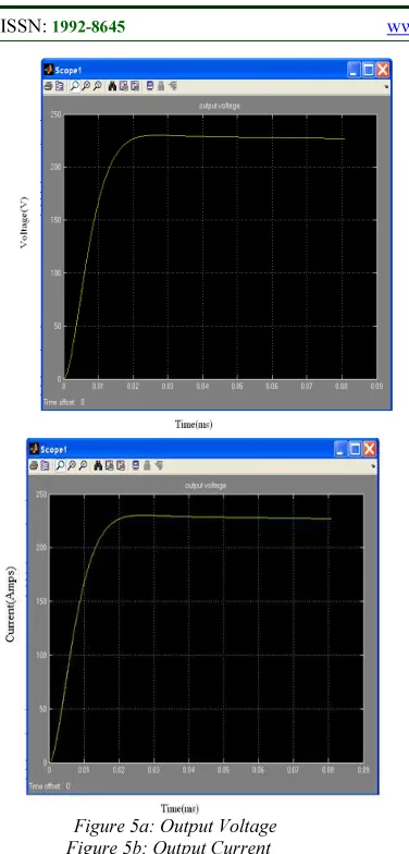
Figure 5a: Output Voltage Figure 5b: Output Current
[image:6.595.88.276.103.495.2]The figure 5a shows the wave form of output voltage, which shows the efficiency of the proposed model. The figure has been generated by connecting output inductor with the capacitor. Also it looks clear that the output voltage will be slowly raised with 230v. The figure 5b shows the wave form of output current, generated by connecting the capacitance and inductance. The MOSFET are serially connected to the circuit so that input current does not vary. At the same time resistance and capacitance are connected parallel to the circuit which provides efficient output with increased voltage.
Table1: The Efficiency Of The Proposed Model In put cur ren t (A mp s) In pu t vol tag e (vo lts) Inp ut po we r (w att s) Ou tpu t cur ren t (A mp s) Ou tp ut vol tag e (vo lts) Ou tpu t po we r (w att s) Lo ss (w att s) Effi cien cy 23 0 0.1 5 34. 500 0
[image:6.595.310.515.316.581.2]230 0.1 45 33. 200 0 1.3 00 0 94.3 3 %
Table 2: Performance Comparisons
Con vert ers Effi cien cy
Buck Boost Cuk GA Cuk In p ut ou tp ut In p ut ou tp ut In p ut ou tp ut In p ut Ou tp ut Pow er in Wat ts
56 42 .4 9
63 56 .5 6 11 8 11 1. 1 14 8. 5 14 5.4 Volt age in Volt s
8 42 .0 6
9 56 20 58 .5 22 .5 52. 94 Cur rent in Am ps
7 1. 01
© 2005 - 2014 JATIT & LLS. All rights reserved.
[image:7.595.91.281.105.274.2]ISSN: 1992-8645 www.jatit.org E-ISSN: 1817-3195
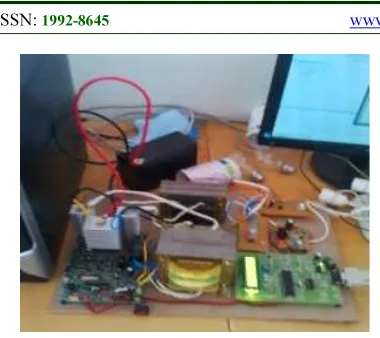
Figure 6: The Hardware Kit Of The Proposed Model
The GA Cuk converter kit has been designed and implemented with the PCB board. The two designed circuit applied to the PCB Board. In the first circuit, the voltage passes through the open loop condition and another circuit connected with the closed loop conditions. So the closed loop condition the output voltage varied by GA cuk controller.
Graph1: The output voltage efficiency of the converters.
0 200
Buk Boost Cuk GA Cuk
E
ff
ii
en
cy
i
n
o
u
tp
u
t
v
o
lt
a
g
e
%
Output Voltage …
From graph1, it is clear that the proposed GA Cuk converter has more output percentage than the others proposed earlier.
Graph2: shows the loss ratio of different algorithms.
0 5 10 15 20
Buk
Boost
Cuk
GA Cuk
L
o
ss
in
W
at
t
s
Loss Ratio
The graph2 shows that the proposed method has less voltage loss compare to other methodologies for the same input current. The graph has been plotted for the input current 230 amps.
5. CONCLUSION
The proposed GA controller based Cuk converter for photovoltaic system was simulated with MATLAB / SIMULINK software. In the proposed model the switching losses are reduced with the help of Genetic algorithm controller and conduction losses are reduced by adapting the MOSFET as auxiliary circuit. The proposed schematic is hard wired to evaluate the performance and has produced efficient results. The GA controller has great impact in selection of MOSFET to conduct the power at each cycle and has produced efficient result in removing the power loss occurred in switching. The proposed design has produced very good results and the output voltage and current produced are high. The efficiency produced by the modular design has been evaluated as 93.33 % which is a successful output.
REFERENCES
[1] Xi Lu, Modularized buck-boost + Cuk converter for high voltage series connected battery cells,IEEE, Applied Power Electronics Conference and Exposition (APEC), pages 2272-2278, 2012.
[2] Wies et al., “Simulink Model for Economic Analysis and Environmental Impacts of a PV with Diesel Battery System for Remote Villages”, IEEE transactions on Power Systems, Vol. 20 [2], May 2005.
ISSN: 1992-8645 www.jatit.org E-ISSN: 1817-3195
IEEE Transactions on Power Electronics, vol. 22, May 2007.
[4] SankarganeshR, Maximum power point tracking in PV system using intelligence based P&O technique and hybrid Cuk converter, International conference on Emerging Trends in Science, Engineering and Technology (INCOSET), pages 429-436 ,2012.
[5] MrudulaY, a high step up dc-dc converter with pv cell for distributed generation system, International Journal of Engineering Research & Technology (IJERT) Vol. 1 Issue 4, June – 2012.
[6] Yu Kang Lo, , Huang-Jen Chiu, Ting-Peng Lee, Irwan Purnama and Jian-Min Wang, "Analysis and Design of a Photovoltaic System DC Connected to the Utility With a Power Factor Corrector", IEEE Transactions on Industrial Electronics, Vol.56, No.11, pp.4354-4362, November 2009 .
[7] Ho-sung Kim, Jong-Hyun Kim, Byung-Duk Min, Dong-Wook Yoo and Hee-Je Kim, "A highly efficient PV system using a series connection of DC–DC converter output with a photovoltaic panel", Renewable Energy, Vol.34, pp.2432–2436, 2009
[8] Athimulam Kalirasu and Subharensu Sekar Dash, "Simulation of Closed Loop Controlled Boost Converter for Solar Installation", Serbian Journal of Electrical Engineering, Vol.7, No.1, pp.121-130, May 2010
[9] Arun K. Verma, Bhim Singh and S.C Kaushik, "An Isolated Solar Power Generation using Boost Converter and Boost Inverter", International Journal of Engineering and Information Technology, Vol.2, No.2, pp.101-108, 2010
[10] M. Vaigundamoorthi and R. Ramesh, "ZVS-PWM Active-Clamping Modified Cuk