VLSI Implementation of 8051 MCU with Decoupling
Capacitor for IC-EMC
Mao-Hsu Yen
1,*, Yih-Hsia Lin
2, Yin-Cheng Chang
3, Yeong-Chang Maa
1, Pei-Jung Tsai
1,
Da-Chiang Chang
31Computer Science and Engineering, National Taiwan Ocean University, Taiwan 2Department of Electronic Engineering, Ming Chuan University, Taiwan 3National Chip Implementation Center, National Applied Research Laboratories, Taiwan
Copyright©2017 by authors, all rights reserved. Authors agree that this article remains permanently open access under the terms of the Creative Commons Attribution License 4.0 International License
Abstract
In recent years, several new methods for IC-level electromagnetic compatibility (EMC) testing have been introduced. Therefore, a handy vehicle for IC-EMC testing is required to validate the effectiveness of the new IC-EMC testing methods. This paper proposes an 8051 MCU for IC-EMC testing platform with in-system programming (ISP) and decoupling capacitor (decap) functions. In order to reduce the EMI and improve the EMC properties for the 8051 MCU, decoupling capacitors (decaps) are added to the integrated circuit (IC) design flow. Chip-level design and fabrication technology are fundamental and cost-effective solutions to this issue. A cell-based design flow is used for chip implementation; specifically, TSMC 90-nm technology is used to implement the present chip via the National Chip Implementation Center. This study will implement two 8051 MCU chips: one that internally comprises a large number of decaps, and another that comprises no decaps. We also implemented an IC-EMC testing platform composed of a multifunction test board and several off-board probes that were fabricated according to IEC 61967 and IEC 62132 standards. The platform demonstrates a method for using the proposed two 8051 chips in EMC testing, and we reveal the results of its EMC performance. Finally, this study simulates the EMC properties, compares the two 8051 MCU chips, conducts static or dynamic analyses for the chips in a power network, and measures the EMC improvements.Keywords
8051, MCU, In-system Programming, Electromagnetic Compatibility, Decoupling Capacitor1. Introduction
The ease-of-use, wide applicability, and high reliability of 8051 microcontroller units (MCUs) has led to their wide-scale application in embedded systems. The 8051
MCU is an 8-bit microprocessor that was developed by Intel in 1980. The 8051 MCU provides such functions as a 4K bytes program memory, 128 bytes data memory, full duplex UART, timers, counters, five types of interrupts, and input/output pins with 32 separate addresses. A conventional 8051 MCU needs to update its firmware in conjunction with an integrated circuit (IC) programmer, and the update operation is time- and labor-consuming. However, an in-system programming (ISP) architecture can shorten the lead time and reduce costs [3]. While the chip area is increasingly small, the number of devices accommodated per unit area is increasing, thus creating more possibilities for EMI [4]. In view of this, a good electromagnetic compatibility solution is a focus of concern. When the power supply voltage drops too low, circuit functionality and performance can be compromised [5]. For instance, in 0.13-μm technology, a 10% voltage variation can result in a 30% variation in the delay of typical gates [6].
The decoupling capacitor (decap) function is widely used to overcome power supply noises. Power supply noises arise mainly from IR drops. Specifically, when all circuits in an IC are turned on/off simultaneously, a high current will be consumed. The consequent IR drop causes a substantial disturbance instantaneously, thus generating power supply noises. Reference [5] analyzes different forms of decap impedance and leakage power, and points out that decaps are suitable to serve as metal fillers in the chip. Because of the frequency response of each decap, high-frequency noises will be connected to the ground plane. When the MCU is operated, any switching would draw current and lead to the noise voltages. Decaps may be temporarily regarded as power supply sources that reduce the noise peaks of noise voltages in the frequency domain. Generally, decaps are expected to offer good IC-EMC solutions that can stabilize the power supply and reduce the high-frequency noises in a power distribution network (PDN).
is implemented on the 8051 MCU to provide a convenient programming method. The ISP carries out serial transmission based on parallel-in/serial-out (PISO) and serial-in/parallel-out (SIPO), thus burning data to the internal Flash or SRAM. The ISP structure implements online programming, and the serial transmission interface reduces the number of I/O pads, and the area of the 8051 MCU. The researchers build an 8051 MCU chip with ISP and decap functions by using TSMC 90-nm technology through the CIC. Finally, this study simulates the EMC properties, compares the two 8051 MCU chips, conducts static or dynamic analyses for them on a power network, and measures the EMC improvements.
In the next section, we describe the architecture of the MC8051 with ISP. In Section 3, we illustrate how to combine decap with 8051 MCU and implement an EMC testing platform. Conclusions are reported in Section 4.
2. 8051 MCU with In-System
Programming
This study developed a new 8051 MCU comprising an MC8051 core and in-system programming (ISP) [2] mechanism. The 8051 MCU is an open-source IP core provided by Oregano Systems [3]. This IP core was
developed jointly by Oregano Systems and the Vienna University of Technology. Its overall architecture is designed by referring to the Intel 8051 and is compiled by using VHDL. Therefore, its order sets are completely compatible with those of the standard Intel 8051, as shown in Fig. 1 (a).
The 8051 MCU herein consists of a microprocessor and a variety of peripherals including timers, general purpose IO (GPIO), communications interfaces, and memory (ROM and/or SRAM). The SRAM of our MCU is generated by using the Artisan SRAM Generator for TSMC. The TSMC SRAM uses a special process and has better area and speed efficiency, thus allowing improvements in overall performance for the 8051.
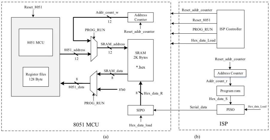
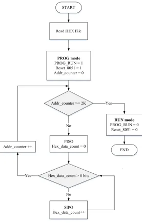
Fig. 1 (a) shows the 8051 MCU proposed herein, and Fig. 1 (b) shows an ISP burning device. The ISP burning device is mainly used to burn data for the 8051 MCU and generates five output signals including Reset_8051, Reset_addr_counter, PROG_RUN, Hex_data_load, and Serial_data. Table 1 describes the control signals of ISP. Figure 2 shows the burning flowchart. The ISP burning device controls the five output signals, copies the “Program ROM” (as shown in Fig. 1 (b)) to the 2K SRAM (as shown in Fig. 1 (a)) in the 8051 MCU, and begins to run the 8051 program. 8'b0 8051_data 8051_address Hex_data_R SIPO Reset_8051 Program rom Reset_8051 Addr_count_r Hex_data_S Serial_data Hex_data_Load PROG_RUN PISO Address Counter 8051 MCU Register files 128 Byte
8051 MCU SRAM_address
SRAM 2K Bytes *.hex SRAM_data PROG_RUN PROG_RUN Reset_addr_counter Hex_data_load 8 8 12 12 12 Addr_count_w 8 ISP Reset_addr_counter ISP Controller Address Counter Reset_addr_counter Hex_data_Load
[image:2.595.79.531.403.638.2](a) (b)
PROG mode
PROG_RUN = 1 Reset_8051 = 1 Addr_counter = 0
START
PISO Hex_data_count = 0
RUN mode
PROG_RUN = 0 Reset_8051 = 0
END Addr_counter >= 2K
Read HEX File
Addr_counter ++
Hex_data_count > 8 bits
SIPO Hex_data_count++
Yes
[image:3.595.175.453.77.513.2]Figure 2. Flowchart of ISP operation
Table 1. Control signals of 8051 MCU with ISP function
Signals Function
Reste_8051 Reset 8051 Reset_addr_counter Reset Address Generator
PROG_RUN PROG mode or RUN mode Hex_data_Load Controls the SIPO and Address Generator
Serial_data PISO data output
2.1. ISP Controller
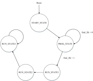
The ISP Controller mainly controls the writing of program data into the SRAM and instructs the 8051 MCU to read and run the program data. This module is designed by using a finite state machine and has five states, as shown in Figure 3. 1. START_STATE
When the reset signal is sent, the ISP controller enters the start state (START_STATE). In this state, the 8051 MCU is
reset, and the SRAM enters the programming state. 2. PROG_STATE
After the MCU enters the programming state, the ISP controller continuously copies the “Program ROM” to the “2K SRAM” in the 8051 MCU. When the 2K SRAM is full, the signal line End_2K is equal to 1; otherwise, the signal line End_2K is equal to 0. When End_2K is equal to 1, the MCU enters RUN_STATE1, preparing to enter the Run mode.
3. RUN_STATE1, RUN_STATE2
Before the Run mode, the 8051 MCU prepares for system switching (PROG mode to RUN mode). At this time, the 8051 MCU is still reset.
4. RUN_STATE3
[image:3.595.59.297.546.640.2]RUN_STATE1
RUN_STATE3 PROG_STATE
End_2K = 1
End_2K = 0 Reset
START_STATE
RUN_STATE2
Figure 3. Diagram of states of ISP controller.
3. VLSI Implementation
In light of Moore’s Law, the number of transistors per unit area of the IC is doubled at regular intervals of 18 months. With the rise in the operating speed of transistors, the instantaneous current per unit time goes up, and the supply voltage required for IC operation decreases year after year. Instantaneous current has become the primary source of EMI. Considering that decaps can provide instantaneous current, decaps are placed near the driver that is close to the power supply terminal and may consume high current in order to reduce power-supply noises [7]. When a high switching current arises, decaps can provide an instantaneous current for the nearby circuit. As a result, this reduces the impacts made by IR drops and L×di/dt, diminishes the fluctuating voltage difference, and stabilizes the voltage of the power supply.
In TSMC 90-nm technology, cross-coupled decaps are used to relieve the electrostatic discharge (ESD) arising from an advanced process [8]. ESD may bring about the breakdown of thin oxides and cause permanent damage to semiconductor devices and computer systems, thus affecting the circuit functions of the IC and causing electronic devices to malfunction. Via the endpoint nodes that connect two transistors, the cross-coupled decaps connect the drain of the PMOS to the gate of the NMOS, and connect the drain of the NMOS to the gate of the PMOS, as shown in Figure 4. Its total capacitance Ceff_overall approximates the standard decap,
while the total resistance Reff_overall is increased significantly.
A parasitic Reff_overall may serve as a resistance to improve
ESD characteristics.
In this study, the 8051 MCU chip is implemented via a cell-based design, and is designed by using a Synopsys design compiler and SOC Encounter [9]. In the process of automatic placement and routing (APR), a filler cell with the decap function is added to the 8051 MCU chip to improve its EMC properties.
VDD
Reff_overall
Ceff_overall VDD
[image:4.595.118.473.86.395.2]VSS VSS
Figure 4. Circuit diagram and equivalent circuit for cross-coupled decap
[image:4.595.317.524.537.667.2]effective resistance of the power cable between the power supply pin and logic units, and the magnitude of the current flowing through the power cable. If the current magnitude is decreased, the impact of the IR drop will be reduced. The decap function can locally adsorb electronic charges and shunt a portion of current. When the local supply voltage is decreased to affect the circuit function, the decap function can also release electronic charges and partly offset the impacts upon logical units made by the voltage drop.
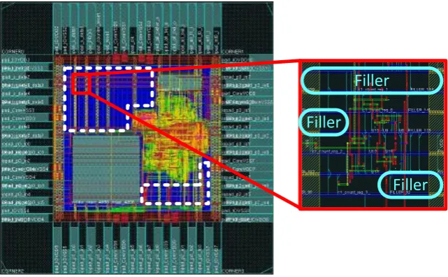
In the process of APR, filler cells are used to fill the gaps between standard cells, thus providing a solution to chip-level EMC (as shown in Fig. 5). Filler cells are used to establish the continuity of the N-well and the implant layers on the standard cell rows, which are primarily nonfunctional cells used to continue the VDD and VSS rails.
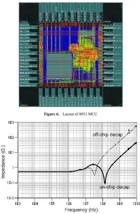
General filler cells possess no capacitance characteristics. To find a good solution to chip-level EMC, filler cells with decoupling capacitance, combined with extended N-wells and P-wells, are used to provide a stable power supply and prevent DRC violations. The fill cells are filled into the chip in descending order. After placement and routing are complete, more than 10,000 decap cells are used. Fig. 6 shows the layout of the 8051 MCU chip implemented by using SOC Encounter. There are 84 I/O pins, the area is 1.0 × 1.0 mm, the voltage used by the internal core is 1.0 V, the voltage used by the external I/O pad is 3.3 V, and the maximum frequency is 200 MHz, as described in Table 2.
After the filler cells with decaps are mounted on the 8051 MCU and undergo placement and routing, the static/dynamic voltage stability of the IC needs to be analyzed for the MCU chip via special software. It has been determined that decaps improves the IC-EMC properties. The capacitance of the implemented chip is as high as 1.6nF, which approximates the capacitance of the decaps on the PCB. In order to demonstrate the improvement of the added decap cells, the VDD-VSS impedance of a testing board which will be introduced in the following section is investigated. The impedance from VDD port of MCU with decap cells is compared with the MCU without decaps but has an equivalent 1.6nF off-chip capacitor. Fig. 7 shows the MCU with on-chip decap cells can reduce the impedance at high frequency. In other words, the decap cells could decouple noise that may cause EMI and EMS issues at chip level more efficient than the off-chip solution.
In addition, a post-layout simulation is conducted by using Synopsys simulation software to analyze the dynamic current characteristics. As shown in Fig. 8, the yellow line is the changing curve of the time domain of the VDD current for the 8051 MCU with the decaps, and the red line is the changing curve of the time domain of the VDD current for the 8051 MCU without the decap function. Compared with the MCU without the decap function, the MCU with decaps that has a current twitch is smaller and has a slower rise in current.
Filler
Filler
[image:5.595.144.465.416.614.2]Filler
Figure 6. Layout of 8051 MCU
[image:6.595.200.412.79.288.2]Figure 7. Comparison of power-ground impedance between on-chip and off-chip decaps.
Table 2. Specifications for 8051 MCU Chip
Items Total
Technology TSMC 90 nm
Area 1.0 mm × 1.0 mm
I/O Pads 84 pins Package CQFP100 Core Voltage 1.0 V
Pad Voltage 3.3 V
[image:6.595.184.426.534.656.2]Figure 8. Difference in dynamic current between chip with and without decap design
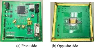
Finally, we design a testing board required by the IC-EMC testing platform for the ISP-capable 8051 MCU. The testing board is designed using specifications in IEC 61967 and IEC 62132 [10], [11]. The testing board is 1.6 mm in thickness and comprises four layers including a ground layer, a power supply layer, a signal layer, and a ground or signal layer. When the elements are laid out, all circuit elements, power connectors, and necessary signal connectors must be soldered on the same side, and the 8051 MCU chip to be measured is separately placed on the other side. We set the coupling network and SMA connector corresponding pins of the wafer on the element-pushing side to test direct coupling by IEC 61967-4 (1 Ω/150 Ω). The testing board for IC-EMC is shown in Fig. 9.
(a) Front side (b) Opposite side
Figure 9. Testing board and 8051 MCU for IC-EMC
4. Conclusions
This study implements an 8051 MCU chip with a chip-level EMC countermeasure. This 8051 MCU chip is an MC8051 version 1.6 developed by Oregano Systems. In addition, an ISP circuit is added so that the 8051 MCU possesses an online burning function. Therefore, the chip does not need to be burned on a specific programmer. As for the transmission of program data, the ISP circuit is connected to the 8051 MCU through PISO and SIPO interface circuit, thus decreasing the number of I/O pads significantly and lowering the manufacturing costs of the chip. As for the
IC-EMC solution, the cell-based design flow incorporates TSMC 90nm technology to implement the 8051 MCU. With the existing APR process, decap fillers are laid out in the remaining space of the chip by using an automated method to reduce the EMI and improve the EMS properties. All of the above design elements are combined to significantly improve the overall operational efficiency of the 8051 MCU.
Acknowledgements
This work received technical and financial support under Contract NO. 2C171050225-44 by Bureau of Standards, Metrology and Inspection (BSMI), Taiwan.
REFERENCES
[1] Yen, M. - H. (2014). VLSI Implementation of 8051 MCU with in-system programming. International Computer Symposium, 308–314.
[2] Oregano Systems (2013). MC8051 IP core user guide. Retrieved from: http://www.oregano.at
[3] Bonnett, D. A. (1999). Design for in-system programming.
IEEE International Test Conference, Atlantic City, NJ, 252– 259.
[4] Lin, C. - R., & Song, Z. - H. (2001). Architecture and principle on conductive EMI measuring system. Micro-Electronics Magazine, September, 186.
[5] Charania, T. (2013). Analysis and design of on-chip decoupling capacitors. IEEE Transactions on Very Large Scale Integration (VLSI) Systems, 648–658.
[6] Pant, S., Blaauw, D., Zolotov, V., Sundareswaran, S., & Panda, R. (2003). Vectorless analysis of supply noise induced delay variation. In Proc. International Conference on Computer Aided Design, 184–191.
[image:7.595.78.279.475.576.2]hot-spot supply noise reduction in ASIC designs. IEEE Journal of Solid-State Circuits, 584–593.
[8] Meng, X. (2008). Layout of decoupling capacitors in IP Blocks for 90-nm CMOS. IEEE Transactions on Very Large Scale Integration (VLSI) Systems, 1581–1588.
[9] Yen, M. - H. (2015). VLSI implementation of 8051 MCU for IC-EMC testing platform. International Conference on
Information Technology and Engineering (ICTAE), 166–173. [10]IEC61967 (2002). Integrated circuits, measurement of
electromagnetic emission, 150 KHz to 1 GHz, international electrotechnical commission standard IEC61967.