1J~@(g] ~
U
@&J::J
[Mt]&~O:JJ&~
MODEL 101AL PRINTER
MAY 1H77
Cen1tronics No. 37400050 Rev. E
I:EnTROnll:S
data computer corp.
iJ§©IM1~U©&lb
[M{J&~
U:JJ&lb
MODEL 101AL PRINTER
MAY 1977
REVISION F
THE INFORMATION CONTAINED HEREIN IS PROPRIETARY AND IS NOT TO BE RELEASED
OR REPRODUCED ~ITHOUT WRITTEN
PER-MISSION OF CENTR!ONICS data computer corp. ;
!I:EnTROnll:s
ft:data
computer corporation
Hudson, New Hampshire 03051
SECTION 1.1 1.2 1.3
1.4
2.1 2.2 2.34.1
4.2
4.34.4
4.54.6
4.74.8
4.94.10
5.1 5.2 6.1 6.26.3
6.4
6.5TABLE OF CONTENTS
SECTION 1
INTRODUCTION
General Description. . . . Logic Flow Diagram (Figure 1-2) Printer Operation . . . . Specifications . . . .
SECTIONS 2 AND 3
INSTALLATION AND OPERATION
Site Preparation (Figure 2-1) . . . . Shipping Crate. . . . Paper Guide and Stacker Assembly (527001001)
SECTION 4
THEORY OF OPERATION
Introduction Basic Timing
I nitializing the Printer. -. Data Input . . . . Shift Register (Buffer) . Character Printing Paper Movement. . . Special Functions Power Supplies
Outputs From LSI Chips.
SECTION 5
REMOVAL, REPLACEMENT AND ADJUSTMENT PROCEDURES
Introduction . . . . Mechanical Assemblies 5.2.1
5.2.2
5.2.35.2.4
5.2.5 5.2.6 5.2.75.2.8
5.2.9
5.2.10 5.2.11 5.2.12 5.2.13Cover . . . . Carriage Mechanism. Driving Mechanism Spring Drum
Damper . . . F rallle. . . . Paper Feed Mechanism Pin Feed Unit . . . . Form Feed Mechanism Ribbon Feed Mechanism. Electrical Hardware. . . .
Paper Stacker And Guide . . . . . Print Head and Associated Assemblies.
SECTION 6
MAINTENANCE
Electrical Adjustments Mechanical Adjustments Preventive Maintenance (P.M.) Troubleshooting Guide . .
Recommended Tools . . . . .
-i-PAGE 1-1 1-2 1-3 1-5 2-1 2-1 2-2 4-1 4-1 4-1 4-4
4-8
4-9 4-15 4-19 4-224-24
5-1 5-1 5-1 5-2 5-5 5-14 5-14 5-15 5-195-21
5-24 5-28 5-34 5-34 5-35 6-1 6-1 . . 6-2 6-46-6
Rev. F SECTION FIGURE 1-1 1-2 1-3 1-4 1-5 1-6 1-7 1-8 1-9 2-1 2-2 4-1 4-2 4-3 4-4 4-5 4-6 4-7 4-8 4-9 4-10 4-11 4-12 4-13 4-14 4-15 5-1 5-2 5-3 5-4 5-5 5-6 5-7 5-8 5-9 5-10 5-11 5-12 5-13 5-14 5-15 5-16 5-17 5-18
TABLE OF CONTEI\ITS
CONTINUED
SECTION 7
DRAWINGS AND LISTS OF MATEFHALS, ELECTRICAL
SECTION 8
DRAWINGS AND LISTS OF MATEHIALS, MECHANICAL
LIST OF ILLUSTRATIONS
Model 101AL Printer (Top Cover Removed) 101AL Printer Logic Flow Diagram
Printing the Letter (H) Print Head Components . . Paper Movement . . . . . Left Front View of 101 A L . Right Front View of 101AL
Rear View of 101 AL . . . . Rear View (101AL Electronics Cavity Removed) Printer Dimensions . ... . . . .
Paper Guide and Stacker Assembly Model 101 A L Block Diagram Prime Timing . . . . Data I nput Timing . . . . Character Timing. . . . Normal and Elongated Characters Print Head Timing . . . . Power Driver Waveform . . . . Line Feed Ttming . . . .
Form Feed and Vertical Tab Timing . . . . VFU Tape Reader Amplifier (Located in VFU) Motor Control Location . . . . Motor Contro( Board I nterconnection Diagram Motor Control Timing. . . . +5V Regulator I nterconnection Diagram. - 12V Regulator I nterconnection Diagram . . Model 101 Series Drive Train . . . . Main Motor Drive and Belt Arrangements . . . .
Determining Backlash Adjustments, Shaft (HB-27). . . . Use of Feeler Gauge for Backlash Adjustment (H B-30, 22). . Bushing End-Play Adjustment for Preload Clutch Shaft (HB-50) Flexible Timing Fence Mounting, Series 101 . . . . Fence Adjustment and Optic Housing. . . . VArtical and Horizontal Alignment of Single Channel f)ptics Housing Location of Left Reed Switch. . . .
Removal of Pin Feed Belt, Idler Slide and Drive Pulley . . . . Adjustment for Paper Holder Gate . . . . . . . . Maintaining 5/8-in. (15.9mm) Nominal Print Margin . . . . Two Adjustments, Gear With Stop Cam (HH-23) and Inside Cam (HH-14) .
Ribbon Feed Mechanism (Rear of Printer, Left Side) Backlash Adjustment, Bevel Gear (H 1-43, 59)
Driving Slide Shaft A - Adjustment . Ribbon Reversing Rod Adjustment.
Ribbon Reverse Timing . . . .
FIGURE 7-1 7-2 7-3
7-4
7-5 7-6 7-77-8
7-9 7-10 7-11 7-12 7-13 7-14 7-15 7-16 7-17 7-18 7-19 7-20 7-2'1 7-22 7-2:3 8-i 8-1 8-2 8-3 8-3A8-4
8-5 8-68-7
8-'8
8-9
8-1 () 8-12LIST OF ILLUSTRATIONS
CONTINUED
Schematic Diagram, Logic/Power Supply +5Volts (Sheet 1) Schematic Diagram, Logic/Power Supply +5 Volts (Sheet 2) Schematic Diagram, Logic/Power Supply +5Volts (Sheet 3)
Schematic Diagram, Logic/Power Supply +5Volts (Sheet 4)
Schematic Diagram, Power Driver Board (Sheet 1) Schematic Diagram, Power Driver Board (Sheet 2)
Schematic Diagram, Video Amplifier . . . . . Schematic Diagram, Power Connections 101AL . Schematic Diagram, Motor Control. . . . Multitap Transformer 50/60 Hz.. . . .
Wiring Diagram, Printer Mechanism. . . . I nterconnection Diagram, Connector Board and Power Supply . . 101 AL Connector Configuration. . . . Component Board Assembly, Logic/Power Supply Board +5Volts .. Component Board Assembly, Logic/Power Supply Board +5Volts Component Board Assembly, Power Driver. . . . Component Board Assembly, Video Amplifier
Component Board Assembly, Connector Card Component Board Assembly, Motor Control Electronic Cavity Assembly. . . .
Harness Assembly (W1) -. . . . . I nput Cable Assembly. . . . Power Cable Assembly (W3)
Mechanical Subassemblies, Series 101 Cover Assembly -" A . . . . Carriage Mechanism. . . . . Drive Mechanism - HB (Part 1) Drive Mechanism - HB (Part 2)
Spring Drum - He
Damper - HD . . . . Frame - HE . . . .
Paper Feed Mechanism . . . . . Pin Feed Mechanism (Left and Right) - HG . Form Feed Mechanism - H H . . . . . Ribbon Feed Mechanism - HI . . . . Print Head and Associated Assemblies (B) .
NOTE
Refer to the Engineering Change Notice (ECN) sheets shipped with the printer for changes made to the prin-ter which have not yet been incorporated into the draw-ings in this technical manual. Always keep these Engin-eering Change Notice sheets with the manual.
Revision IIBvel indications at the lower right-hand corner of a page reflect at what revision of the manual that page was updated.
-iii/iv-PAGE 7-2 7-3
7-4
7-5 7-6 7-77-8
7-9 7-10 7-11 7-12 7-137-14
7-15 7-16 7-19 7-21 7-23 7-25 7-27 7-29 7-31 7-33 8-2A 8-3 8-58-7
8-9
8-11
8-13 8-15 8-178-19
8-21 8-23 8-26SECTION 1 INTRODUCTION
This manual describes the Model 101 AL printer, manufactured by Centronics Data Computer Corporation. It provides general information, detail~d theory of operation and maintenance information enabling field service personnel to maintain the printer. For serial input or other detailed interface infor-mation, a separate document for each interface is published for your reference.
The manual is grouped into eight sections, each with its specific purpose.
Section 1 - INTRODUCTION, introdwces the reader to the scope and content of the
Section 2
Section 3
Section 4
Section 5
Section 5
Section 7
Section 8
manual, and provides the reader with a general description of the printer.
- INSTALLATION, contains unpacking and installation instructions for the printer.
- OPE RATION, describes the function of all operator controls and indicators and how they are used.
- THEORY OF OPERATION, contains
a
detailed description of each major opera-tion performed by the printer electronics, including timing diagrams and, where applicablH simplified circuit diagrams, all keyed to the schematic drawings.- REMOVAL, REPLACEMIENT AND ADJUSTMENT PROCEDURES, includes step-by-step removal and replacement procedures for all major assemblies and sub-assemblies in the printer.
- MAl NTENANCE, includes preventive and corrective maintenance procedures and a maintenance schedule.
- ELECTR~CAL DRAWINGS AND LIST OF MATERIALS, contains a complete set of schematic, wiring and component board layout diagrams and their associated list of materials for the electrical portion of the printer.
- MECHANICAL DRAWINGS AND PARTS LISTS, includes all printer assembly drawings and their associated parts lists for the mechanical portion of the printer.
At the end of the manual are several appendices which include a glossary of signal mnemonics, a standard
9 x 7, 54-character set, and parallel interface specifications.
1.1 GENERAL DESCRIPTION
The Model101AL printer (Figure 1-1) is a medium speed impact printer which uses a 9 x 7 dot matrix for character generation. The unit prints at a rate of 155 characters per second with an average speed of 132 characters per second (including the return time for the printing head). The printer is capable of printing 132 columns, with paper width varying from 4 inches to '14-7/8 inches. The unit uses sprocket-fed paper and gen-erates 5 lines to the inch vertically with 10 characters per inch, horizontally. The printer does not require spe cial paper and can produce one original plus four copies.
The printer is completely self-contained. A singile printed circuit board contains both the control logic and power supplies, made possible by the use of LSI (Large Scale I ntegration) circuitry.
Figure 1-1. MODEL 101AL PRINTER (TOP COVER REMOVED)
1.2 LOGIC FLOW DIAGRAM (Figure 1-2)
If the input device transmits serial data (100-9600 Baud) then an optional RS232 interface is re-quired to assemble the serial data, then transfer it in parallel to the input buffer in the printer.
Paper movement is initiated by a line feed, vertical tab and form feed function. The Vertical Format Unit (VFU) tape reader provides vertical tab and top of form spaeing control by means of a perforated paper tape. I n addition, the printer recognizes the following special control codes: bell,delete, select, de-select and elongated character, as described in Section 1.3.3.
Once a line of printable characters is stored in the buffer, head motion is initiated by activating the forward clutch, causing the print head to move from left to right across the paper. With the head in motion, data is transmitted from the buffer to the character generator. From there, character write pulses are sent to the driver circuits, which energize the print head solenoids causing the print wires to form the characters on the paper.
Rev. E
DATA
INPUT
-
-TIMING VFU OPERATOR
TAPE BUZZER
FENCE
READER PANEL
• •
t
,
CONTROL HEAD MOTlON_ CLUTCH/
CONTROL
-1. PRINT COMMAND (CR OR LAST CHAR.)
PAPER MOTION_ PAPER
2. PAPER MOVEMENT ~ MOVEMENl"
(LF, VT, FF) CONTROL SOLENOID
3. SPECIAL FUNCTIONS
(BEL~DELET~EX~ TIMING CHAR)
1
SHIFT
- ' CHJlIRACTER
I
WRITE_J
PRINT1
-
-
REGISTERI
GENERATORJ
PULSES"I
HEAD BUFFERFigure 1-2. 101AL PRINTER LOGIC FLOW DIAGRAM
1.3
PRINTER OPERATIONBasically, all printer functions can be grouped into one of the following three categories: 1) character printing, 2) paper moveme.nt, and 3) other auxiliary functions such as printer select/de-select, delete, etc.
1.3.1 CHARACTER PRINTING
A small aluminum carriage supports the print head assembly. During printing operation, the car-riage travels along the print line from left to right at a constant rate of approximately 16.25 inches per second, and returns in approximately 240 milliseconds.
Printing is accomplished by selectively firing the print wires. These wires graphically construct the characters out of dots, as the print head moves from left to right across the print line.
Printing impulses energize the print solenoids and drive the print wires against the ribbon, paper and platen to form the characters in a dot matrix pattern. When the solenoids are de-energized, the wires are withdrawn so they are flush with the surface of the jewel. Each solenoid can fire independently up to five times for anyone character. Figure 1-3 is an example of the dot matrix forming the letter H. All character formations in the standard 9 x 7 dot matrix are shown in Appendix B.
PRINT HEAD JEWEL
Figure 1-3. PRINTING THE LETTER (H)
PRINT WIRES
A
Figure 1-4. PRINT HEAD COMPONENTS
The print head (Figure 1-4) consists of the jewal, casting and seven solenoids with attached print wires. The seven print solenoids and their attached print wires are arranged around the print head. The free
ends of the print wires pass through a wire guide at the front of the print head, which properly spaces the wires so that the correct wires passes through the correct hole in the print jewel.
Printing action is initiated when the input buffer has been filled or a carriage return (CR) character has been received. The print head then sweeps across the page until a CR command is decoded at the buffer out-put or the head reaches the 132-column limit right li'mit switch. At this time, the print head returns to the left margin and an automatic line feed is performed. As as an option, the automatic line feed can be disabled.
1.3.2 PAPER MOVEMENT
Paper can be moved manually by rotating the platen knob (shown in Figure 1-5) or automatically by any of three paper movement commands: line feed, vertical tab and form feed.
Rev. E
FORM FEED (RELEASE)
CLUTCH
Figure 1-.5. PAPER MOVEMENT
10183
A small independent motor not shown in Figure 1-5, provides the power necessary to move the sprocket-feed tractors which control paper movement. To move the paper, the printer electronics activates a line feed solenoid which activates a clutch that mechanicallv links the motor to the sprocket-feed tractors.
To initiate a single line feed, the line feed solenoid is energized for 15 milliseconds to initiate paper motion. Upon completion of the line feed command, a 60 millisecond delayed line feed is generated. This allows the clutch pawl and clutch mechanism to return home before another line feed is allowed.
Vertical forms movement is accomplished by applying a DC level to the paper feed solenoid until a hole is detected in the Vertical Format Unit (VFU). The tape consists of two channels; one used for Top of Forms and the other for Vertical Tab. The movement of the paper tape is caused by direct mechanical lin-kage to the gear train which drives the paper feed tractors.
When the printer runs out of paper, a sensing switch activates a two-second audible tone in a speaker located in the rear of the printer. The printer also stops printing and lights the PAPE R EMPTY light on the control panel.
1.3.3 SPECIAL FUNCTION
I n addition to the printable characters shown in Appendix B, the printer can recognize the following special functions:
Carriage Return (Octal 015) - I nitiates the printing of a line.
Form Feed (Octal 014) -Moves the paper until the top of the form hole in Tape Reader Channel 7 is reached.
Vertical Tab (Octal 013) -Moves the paper until the next hole in Taper Reader Channel
5
is reached. Line Feed (Octal 012) -Advances the paper one line.Delete (Octal 177) -Primes the printer electronics to an idle state and deletes any characters stored in the printer.
Bell (Octal 007) -Generates a two-second audible tone in the speaker at the rear of the printer. Select (Octal 021) -Allows printer to receive data, same as activating SE LECT switch.
De-Select (Octal 023) - I nhibits printer from receiving data, same as deactivating SE LECT switch.
1.4 SPECIFICATIONS
Printing Method:
Printing Rate - Characters: - Full Lines: - Short Lines: Transmission Rate - Serial:
- Parallel: Data Input:
Character Structure: Code:
Indicator - Switch Controls:
Indicator: Manual Controls: Character Buffer: Format:
Paper Feed: Paper:
Number of Copies: Dimensions: Weight:
E!ectrical Requirements: Temperature - Operation:
- Storage: Humidity - Operating:
- Storage: Standard Features:
Optional Features:
1.5 PHYSICAL DESCRIPTION
Impact, character-by-character, one line at a time. : 165 characters per second
:55
±.
5 lines per minute (132 character line) i200 lines per minute (20-30 characters) '100 to 9600 baud (with Serial option) ,See Timing Diagram - Appendix B ;Parallel (Serial option available):9 x 7 dot matrix, 1 O-point type equivalent
:USASCII - 64 characters printed, lower case characters irecognized and printed as upper case equivalent.
:ON/OFF, SELECT, TOP OF FORM, FORMS OVERRIDE, ,LINE FEED.
PAPER OUT
:Form Thickness, Paper Advance Knob :132 characters (1 line)
132 characters maximum per line, 6 lines per inch. Sprocket feed, adjustable from
4"
to 14-7/8" width. Standard sprocketed paperOriginal and up to four carbon copies 11
%"
high,20"
deep,27%"
wide 118 pounds115 VAC
±.
10% 60Hz or 115/230 VAC±.
10% 50 Hz.40"
to 1 00° F-40"
to 160"
F5% to 90% (no condensation) 0% to 95%
Vertical Format Control Audio Alarm
Elongated Boldface Characters Paper Runaway Inhibit
$eparate Prime Line and Fault Line to Output Connector 'Remote Select/De-Select
Automatic Line Feed Disabled.
Character sets of 64,96, or 128 characters Popular parallel and serial interfaces Automatic motor control
Selectable single character elongation f=lapsed time indicator
The printer is approximately 11 %" high,
20"
deep,27-%"
wide and weighs approximately 118 pounds. Figures 1-6 through 1-9 are photographic views ofthe
printer taken with the covers removed. Each major printer assembly is located on these figures and ideritified in the table below the photo.1. Print Head Assembly 2. Carriage
3. Form Feed Mechanism
1. Operator Control Panel
Rev. E
2. Form Feed Motor 3. Video Amplifier and
Cable Assembly 4. Light Source
4. VFU Tape Reader 7. Spring Drum 10. Timing Fence
5. Pin Feed Mechanism 8. Platen Knob 11. Main Drive Belt
6. Ribbon Feed Mechanism 9. Damper
Figure '1-6. LEFT FRONT VIEW OF 101AL
5. Optical Pick-Up 9. Penetration Control Knob
6. Optic Bundle 10. Forward Clutch
7. Ribbon Cable 11. Maiin Pulley and Drive Belt
8. Power Driver Board 12. Re"erse Clutch
Figure 1-7. RIGHT FRONT VI EW OF 101AL
1-6
13. Cooling Fan 14. Ribbon Feed
1. Connector Card 2. Connector J4 3. Connector J6 4. Connector J3 5. Connectlor J2
1. Main Motor
2. Motor Starting Capacitor 3. AC Power Connector
6. J1 7. FuseF5 8. AC Power Input 9. +30V Power Supply 10. Fuse F4
Figure 1-8. REAR VIEW OF 101AL
4. Electronics Connector 5. Power Transformer 6. Power Distribution
11. . Logic/Power Supply Board 12. Speaker
13. Electronics Cavity
14. Input Connector
7. 8.
Ribbon Reversing Rod Ribbon Drive Rod
Figure 1-9. REAR VIEW (101AL ELECTRONICS CAVITY REMOVED)
SECTIONS 2 AND 3
INSTALLATION AND OPERATION
A separate operators manual (No. 37400001): contains most of the installation, set-up and operating procedures for the Series 100 printers. This operators manual should be referred to during normal printer installation and operation.
Included on the following pages is additional ,information not contained in the operators manual.
2.1 SITE PREPARATION (Figure 2-1)
A line drawing of the printer dimensions is shown in Figure 2-1. As shown in this drawing, the width of the installation site must take into account the side covers in an opened position.
;?~~~f~~
111111111111@
~
~~====20="(=50=,8=cm=)==~~~L---27,7"(70,~cm)
---1
Figure 2-1. PRINTER DIMENSIONS
Enviromental and electrical requirements at the installation site are as follows:
Temperature:
Humidity:
Electrical:
2.2 SHIPPING CRATE
40° to 100° F (Operating) -40° to 1600 F (Storage)
5% to 90% (no condensation) - Operating 0% to 95% - Storage
115 VAC ±.10%, 60Hz, 3 amps 115/230 VAC ±.1 0%, 50Hz, 1.6 amps
The printer is shipped in a crate approximately.20 inches high, 27 inches deep and 32 inches wide. The crate is made of weatherized, triple-,walled cardboard. When properly strapped, the packing crate and printer is capable of fork lift operation with a seven-high stacking capability.
Shipped with the printer are the following items:
(1) If a special interface is used, the interface card is included with the printer. For certain interfaces such as the RS232, a special cable is also shipped. Cabling requirements for the standard parallel interface are defined in Appendix B.
Rev. E
(2) A standard vertical format paper tape providing six line feeds (one inch) for each vertical tab and 66 line feeds (11 inches) for each form feed code. This tape is a part of the ver-tical format unit. Refer to the Operators Manual for duplicating the exixting tape, or if a different format is desired, for generating a new tape.
(3) Documentation - All documentation describing that particular printer is included in a plastic under the printer. This documentation includes a teehnical manual for the printer and any optional interface, and a notice of all approved changes incorporated in the printer but not documented in the manual. Please keep this documentation with the printer at all times so that accurate information will be available for troubleshooting purposes.
(4) Pin Feed Knobs - These knobs are contained in a small plastic bag stapled to the guide bar for the pin feed unit.
(5) Print Sample - A sample printout from that particular printer is included in the upper paper pan.
(6) Unpacking/Repacking and Set-up I nstruction Sheet.
Shipped in a separate container is the paper guide and stacker assembly. I nstallation instructions for this assembly are included with the assembly and also in St3ction
2.3.
2.3 PAPER GUIDE AND STACKER ASSEMBLY (5270010101)
ASSEMBLY INSTRUCTIONS
Attach paper guide and stacker assembly (one piece) to the back, top of printer by first removing two screws from the left and right side, and install using a flat bladed screwdriver. Make sure rounded pa-per guides rest on top of printer in front of papa-per feed opening.
ATTACHING SCREWS
STACKER GUIDE! TRAY
PRINTER STAND OPERATION
,,}'RINTER STAND
TABLE TOP OPERATION
Figure 2-2. PAPER GUIDE AND STACKER ASSEMBLY
SECTION 4
THEORY OF OPERATION
4.1 INTFtODUCTION
This section on the theory of operation contains a detailed description of each major function performed by the Model 101 A L printer electronics. Figure 4-1 shows a basic functional diagram of the printer electronics.
Throughout this section, reference is made to the schematic diagrams contained in Section 7. The section is organized as follows:
Paragraph 4.2 Basic Timing
4.3 I nitializing the Printer (Prime, Select)
4.4 Data Input (Data, Strobe, Busy, Acknowledge)
4.5 Shift Register (Buffer)
4.6 Character Printing
4.7 Paper Movement (Line Feed, Vertical Tab, Form Feed)
4.8 Special Functions (Bell, Paper Empty, Delete, Motor Control)
4.9 Power Supplies
4.10 Outputs from LSI chips
4.2 BASIC TIMING
The basic timing clock for the printer electronics is derived from signal OSC. This OSC signal is generated on LSI chip ME9 pin 25. The frequency of OSC, determined by the RC circuit (R41-C9) on pin 26 of this chip, ranges from 100 to 200 KHz.
This OSC clock is then used by both LSI chips (ME5 and ME9) for internal timing, and is in-verted by M E4-6 to generate OSCXT. Signal OSCXT goes to the printer interface connector and if an optional interface is used, it also goes to this optional interface board (e.g., RS232 Serial I nter-face).
4.3 INITIALIZING THE PRINTER
Before the printer can accept input data, it must first be PR I ME'd and SE LECT'ed. The prime operation initializes the printer logic to a ready state. The select operation after causing a prime con-dition, (which can be disabled by jumper (E14-E15~, resets the busy line to the interface connector and makes the printer ready to receive data.
4.3.1 PRIME
The PR I ME signal, generated on LSI chip ME9-37, is generated by any of the following con-ditions.
A. Power Turn-On - When the printer is turned on, capacitor C17 is initially discharged causing a low 100-500 msec PWRPRM signal into 32. This generates a high PRIME signal at ME9-37. As C17 charges to +5V, PWRPRM goes high terminating the power prime operation.
INTERFACE CONNECTOR
r---.
I LOGIC/POWER SUPPLY BOARD I
, PRINT WIRE ,
I
PARALLEL DATA INPUT I (DSl - DS8) I:>
SHIFT REGISTERTB1-T88 ~ CHARACTER GENERATORS
V
CONTROL CGl-7 , ~
V
~r-v
SOLENOIDS TO PRINT HEAD 8 x 133j ~.
CLKTB2, SRCL, PRIME iii ~ ~ .oJ u PAPER MOVEMENT
-I INPUT PRIME,DATA STROBE LSI CHIP NO.1 _ CONTROL .. I
I ACKNOWLEDGE. BUSY I (DATA DECODE)
r
-I
!I
II
:
I
L _ _ _
BUZZER
-r-VFU TAPE VTH. FFH READER
c
Z en
<t a:
en 0
w ~
1: <t u u
~
0en ~
~ OPERATOR PANEL (ROM's)
•
o:r 9 0 3: u cC!:I ~.
Z
:E
;:
~ u C
LSI CHIP NO.2 (PRINT CONTROLl
PMSOL
FWD CLUTCH CIP
REV CLUTCH CIR
-
-DRIVER CIRCUITS
~ TO LINE FEED SOLENOID
~TOFORWARD
CLUTCH
-
i1
- "'----_
..
,
TO REV CLUTCH STROBE
DLYSTB
STROBE ... - ... _ VIDEO AMP ONE-SHOTS
___________ ...1
RTPSW. EOPSW LIMIT SWITCHES
B. PrinterSelection-lfthe Delete Inhibit option (DELlNH) is not used (i.e., jumper E13to E14 is connected), then a low SLCT input to ME9-40 and a high DELINH to ME9-39 gen-erates a 100-400 usec PRIME pulse at ME9-37.
C. End of a Printed Line - At the end of a line of print, CI PX at ME9-30 goes high, turning off the forward clutch and generating a 100-400 usec PRIME pulse at LSI chip ME9-37.
D. Delete Code - Receiving a delete code (octal 177) * on input data lines 551-DS7 generates a low DCPRM output at LSI chip ME5-8. Signal DCPRM then generates a 100-400 usec PRIME pulse out of LSI chip ME9-37.
E. Input Prime - Reception of a low INPUT PR I ME level at the interface connector generates a high IP signal into LSI chip ME5-36. This produces a low DCPRM output at LSI chip ME5-8 (same as the delete code), which in turn generates a 100-400 usec PR I ME pulse out of LSI chip ME9-37.
In all of the above cases, the high PR I ME signal out of LSI chip ME9-37 resets the printer logic including the shift register and places a dummy character in the first character position in the register. A diagram of the prime timing is shown in Figure 4-2.
PRIME_--..F ... - - - . . - - - 100-400 us .. ,
! I -I
I
SRCL _ _ _ ....
r
;
L_
LOAD DUMMY CHARACTER
*'
I
- 8usec
I CLKTB2
I
20-30 us .. ~ ~
Figure 4-2. PRIME TIMING
The high PR I ME signal into pin 3 of the two shift register elements (ME 18 and ME 19) disables all inputs to these elements and internally resets all stages of the shift register. When PR I ME goes low, recirculate signal SRCL from LSI chip ME9-38 remains high and a single CLKTB2 pulse is generated at ME9-36. The high SRCL (and low PRIME) connect shift register outputs TB1-TB7 back to inputs DS1-DS7, and enables a high (+5V) input to stage 8. Note that since the shift register uses inverted signals for both inputs and outputs (e.g., DS 1 and TB 1), a high input to stage 8 represents a ZE RO into that stage.
The single CLKTB2 pulse then clocks a dummy character into the register (i.e., ON ES into stages 1-7 and a ZERO into stage 8).
*Throughout this section, input codes are defined only by their first seven bits. However, bit 8 into the function decoder contained in LSI chip 5 must be a ON E.
Rev. E
4.3.2 SE LECT
Before the printer can receive data, it must first be selected. This can be done either by the SE LECT switch on the operator panel or by an octal 021 code on the input data lines.
Pressing the SE LECT switch (S4) generates a low SE L.SW signal into LSI chip ME5-31. The chip contains lIanti-bounce" protection which requires the SE LSW line to be noise-free for approx-imately 2-8msec before the level is recognized by the chip. Aft~r this delay, the low SE LSW input sets a Select latch in the chip. The output of this latch appears as signal SLCT' on LSI chip ME5-40.
Similarly, a decoded octal 021 code on data inputs D~fi -DS7 AN Oed with ungated data strobe pulse DST A also sets this Select latch.
The printer is deselected (i.e., the internal Select latch is reset) either by again pressing the SE LECT switch or by an octal 023 on data lines DS1-DS7 and a DSTA pulse. Alternately pressin~the SELECT switch alternately selects and deselects the printer. Note that when power is turned on,WRPRM resets the internal Select latch so that the printer initially appears in a deselect state.
A high SLCT' signal at ME5-40 indicates that the printer is selected. This signal, inverted by ME22-6 (SLCT) turns on the SELECT lamp on the operator panel. SLCT inverted by ME20-4 generates a SLCT signal to the interface connector.
If DE
LI
NH
jumper E 13 to E 14 is connected, then selHcting the printer will also cause a prime con-dition. If jumper E 14 to E 15 is used, select will not cause a prime concon-dition.4.4 DATA INPUT
Inputs to the printer consist of seven standard parallel data lines (DATA1-DATA7), an optional DATA8 line, an active low DATA STROBE input, and an active low INPUT
PR I
ME line. The first seven data lines represent the 7 bit ASCII code shown in Appendix B. The optional eigth bit is used as a control bit either for specifying an elongated character or for selecting an additional character set. The data strobe is used to synchronize the input data with the printer electronics. The prime line is used to prime (initialize) the printer electronics.The eight data inputs have a unity loading factor and are terminated by a 1 K pull-up resistor to +5volts. The data strobe and prime inputs are terminated by a 470 ohm resistor to +5 volts. Note that with no input on DATA8 line, terminating resistor R 15 holds the input at +5V, making bit 8 appear as a ON E on the logic card.
I n response to received data, the printer generates an Acknowledge pulse to acknowledge recep-tion of a character. If the received character caused the printer to perform some funcrecep-tion such as paper movement, character printing, etc., the printer responds wi1th a Busy signal.
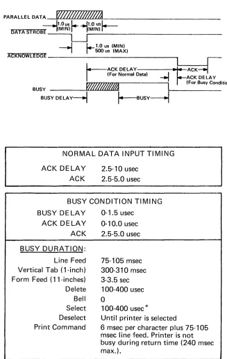
4.4.1 DATA INPUTTIMING
I n general, the data transfer sequence consists of the input device placing the appropriate code on the data lines to the printer and then generating a data strobe pulse. The printer, after a slight delay, responds with an acknowledge pulse. Or if the received data caused a busy condition, the printer first activates the busy line for the duration of the busy condition and then responds with an acknowledge pulse.
If the received data does not cause a busy condition, the printer generates a 2.5 to 5.0 usec ACKNOWLEDGE pulse (some 2.5 to 10 usec after the trailing edge of DATA STROBE) indicating that it is ready to receive additional data.
If the received data causes a busy condition, the busy signal goes active 0 to 1.5 usec after the trailing edge of DATA STROBE, and the ACKNOWLEDGE pulse is generated 0 to 10 usec after BUSY is terminated.
The ligated strobe" feature in the 101 A L prevents the printer from recognizing a data strobe unless the previous character has been acknowledged. A non-gated data strobe option, is available however to allow the printer to accept all data strobes. A data transfer timing diagram is shown in Figure 4-3.
PARALLEL DATA
~J.%I~hf~
DATA
STROB~lJtNS)r- ---I1Jt~i~
--~~---1
L-
1.0 us (MIN)-,
r
500 us (MAX)ACKNOWLEDGE
i.----ACK DELAY
~~ACK~
I
(For Normal Data)-..J
ACK DELAY .BUSY W#l~
I
(For Busy Condition)BUSY DELAy----I
r----sUSY~
NORMAL DATA INPUT TIMING
ACK DELAY ACK
2.5-10 usec 2.5-5.0 usec
BUSY CONDITION TIMING
BUSY DELAY ACK DELAY ACK
BUSY DURATION:
Line Feed Vertical Tab (1-inch) Form Feed (1 'I-inches) Delete Bell Select Deselect Print Command
0-1.5 usec
0-10.0 usec 2.5-!5.0 usec
75-105 msec 300-310 msec 3-3.5 sec 100·400 usec
o
100-400 usec
*
Until printer is selected
6 msec per character plus 75-105 msec line feed. Printer is not busy during return time (240 msec max.).
[image:22.611.145.472.99.616.2]*
No busy if inhibit prime on select option is used.Figure 4-3. DATA INPUT TIMING
Rev. E
4.4.2 BUSY
A busy indication is developed by LSI chip ME5 pin 11" This BUSY output, normally high when the printer is not busy, goes low when any of the following conditions occurs:
(1) CSBSY goes low - This occurs when a dummy character (TBB) is detected at the shift register output and a prime operation is not in progress. This indicates that the 132nd character has just been loaded into the shift register (without a carriage return code).
(2) PR I ME goes high - This occurs during a prime operation as described in Section 4.3.1.
(3) LFF (internal to ME5) goes high - This occurs either when a form feed code (octal 014) is received, or if the optional TOP OF FOFtM switch on the operator panel is pressed. (Note: If the DSC option is used, the receiived F F code will first cause the line to be printed before activating LFF). LFF is nOI~mally reset by the trailing edge of DL YLF.
(4) LLF (internal to ME5) goes high - This occurs when a line feed code (octal 012) is received or the optional LINE FEED switch on the operator panel is pressed. LLF is reset by the trailing edge of DL YLF.
(5) L TF (internal to ME5) goes high - (Similar to the LFF signal) - L TF goes high when a vertical tab code (octal 013) is received and is reset by the trailing edge of DL YLF.
(6) DCPRM goes low - This occurs: (a) when a delete code (octal 177) is received, or (b) when an JNPUT PRIME signal is received at the interface connector, or (c) a power
prime (PWRPRM) condition exists.
(7) R EMCR (internal to ME5) goes high - This occurs when a control character is clocked into the shift register, indicating the start of a character printing operation. I n the
standard 101 A L printer, only the carriage return control code (octal 015) is stored in the shift register. However, if the DSC option is used (jumper E10 to E11), then a LF, VT, F F, or CR code (octal 012, 013, 014, and 015 respectively) may be loaded into the shift register.
(B) PMSOL goes low - This occurs while the paper movement solenoid is activated.
(9) FAU L T goes high - This occu~ (a) if the printer is deselected (S LCT' is low), or (b) if the printer is out of paper (PE is low), air (c) during a paper time-out condition, or (d) during a Light Detect (LD) error condition. LD goes low if no video signal is detec-ted as the print head travels across the page.
(10) DL YLF goes high - This 60-90 millisecond line feed delay occurs following a paper move-ment operation.
As shown in the timing diagram in Figure 4-3, BUSY can occur up to 1.5 usec following the trailing edge of DATA STROBE. The worst case (1.5 usec) condition arises when CSBSY goes active. This occurs because of the accumulated delays in loading the 132nd character in the shift register, detecting the dummy character at the output, generating the CSBSY on LSI chips ME 16 and finally generating the BUSY on LSI chip ME5.
4.4.3 FUNCTION DECODER
The buffered data inputs are applied to a function decoder on LSI chip ME5. These data lines gated with a data strobe signal are decoded and if a control code is detected, specific functions occur as de-cribed in Table
4-1.
Table 4-1. CONTROL FUNCTIONS
,-Octal Output
Function Code Jumpers Strobe Mnemonic Printer Action
Bell 007 None Gated BELL Generates an audible tone, 1 to 2 seconds in duration, in the speaker of the printer.
_._---Line Feed * 012 None Gated CSLF, Advances the paper one line. PMSOL
-.--
-Vertical 013 None Gated PMSOL Causes paper to advance until the
Tab* next hole in channel 5 of the
Vertical Format Unit (VFU) paper tape is reached.
-Form 014 None Gated PMSOL Causes paper to advance until the
Feed* next hole in channel 7 of the VFU
paper tape is reached.
-
,-Carriage 015 None Gated DSCR Causes the received line of characters
Return to be printed.
-Elongated 016 E16-E18 Gated UPSC Causes all characters on the line to
Character be printed at double the normal width.
-Select 021 None Ungated SLCT' Selects the printer. E 14 to E 15 inhibits a prime operation during select.
Deselect 023 None Ungated SLCT' Deselects the printer.
Delete 177 None Ungated DCP~M Primes the printer.
*If the DSC option is used (jumper E10 to E11), LF, VT, and FF also cause the received line of characters to be printed.
I n addition to the functions listed, the function decoder also monitors the input data for the first printable character (i.e., a ONE in bit 6 or
7).
Detection of the first printable character, sets First Character Clock latch (FCCLK) internal to LSI chip ME5. Only when this latch is set will the printer respond to a carriage return code (or if the DSC option is used, to a LF, VT, or F F code) by printing the line of characters.4-7
,
Rev. E
4.5 SHI FT REGISTER (BUFFER)
The printer storage buffer consists of two quad 133-bit shift register MOS elements (ME16 and ME 17). These elements provide an 8 x 133-bit storage capacity or one full line of 132 characters. The extra character storage (i.e., 132 instead of 133) is used for storing a dummy character ( a ON E in bit 8). Detection of this dummy character at the shift register output indicates that the 132nd character for that line has just been shifted into memory.
A high PRIME input to ME16 and ME17, disables all other inputs and asychronously resets the entire register. When PRIME is low, the shift register operates in either the normal or the recirculate mode. With the recirculate input (SRCL) low, each CLKTB1 or CLKTB2 pulse clocks the DS1-DS8 inputs into the shift register. With SRCL high, the register is in the recirculate mode. The first three stages in each shift register element are recirculated internally. The fourth stage in ME 17 is recirculated by the external connection TB4 to the Recirculate Input (R.I.). ThH R.I. terminal for the fourth stage in ME17, however, is tied to +5V. As a result, when the SRCL input is high, CLKTB recirculates the TB1-TB7 outputs back to the inputs and forces a ONE into the eighth stage (TB8).
The actual shift register timing depends on which of the following printer operations is taking place: 1) a prime condition; 2) data reception 3) reception of a carriage return code (octal 015) prior to the 132th character in a line; or 4) printing a line of characters.
(1) Priming the Shift Register
During a prime condition, LSI element MEg generates a high PRIME signal. While PRIME is high,.ill shift register stages are automatiically reset, independent of the data inputs. After PRIME goes low, SRCL remains high and a single CLKTB1 pulse is generated. At this time, a ONE is clocked into bit 8 (due to +5V at the recirculate input ME16 pin 15), generating a dummy character at that location.
(2) Normal Data Input
(3)
(4)
During normal data input from the external device, LSI element ME5 generates a CLKTB1 pulse, slightly delayed from data strobe, each time a printable character or a CR code has been received. The trailing edge of CLKTB1 then clocks data lines DS1 - DS8 into the shift register.
Following a Carriage Return Code
Following the reception of a carriage return code, LSI chip ME 16 generates CLKTB2 pulses to the shift register, at the same rate as the OSC clock. This shifts the register until the dummy character appears at the output (TB8 goes high). The high TB8 then terminates the CLKTB2 pulses.
During Character Printing
When printing a line of characters, during E!ach DCWO interval (developed internally in LSI chip MEg), the video STROBE pulse generates a CLKTB2 pulse. This clocks the next consecutive character to the output of the shift register, where it remains until the next DCWO - STROBE interval.
4.6 CHARACTER PRINTING
When the dummy character appears at the shift register output (TB8), other than during a prime condition, the logic activates an electromechanical clutch which causes the print head to move from left to right across the page.
As the print head carriage moves across the page, the timing fence (and light source) generate timing inputs to the video amplifier board. These timing signals are used by the logic to register the five full columns of dots in the printed character.
The logic uses two ROM (Read-Only Memory) elements for each character set. One ROM defines the dot pattern for the five full-step columns, the other defines the dot pattern for the four half-step columns in a g x 7 matrix.
This section describes the character printing operation in the following sequence.
Paragraph 4.6.1 I nitiatling the Printing Operation 4.6.2 Character Registration and Timing 4.6.3 Character Generator (ROM) 4.6.4 Print Head Operation 4.6.5 Power Driver Circuits
4.6.1 INITIALIZING THE PRINTING OPERATION
As data is received by the printer, the dummy character is shifted through the shift register. As the 132nd character is received, the dummy character appears at the shift register output. I f a carriage return code (octal 015) is received before the 132nd character, this code is stored in the register and lSI chip MEg generates ClKTB2 pulses to shift the register until the dummy character appears at the output. A high TB8 indicates dummy character.
When TB8 goes high, lSI chip MEg generates a low CIPX signal. CIPX is inverted by ME10-2 to gen-erate CIP, which is in turn inverted by ME6-12 to gengen-erate
Cif5.
The high CI P signal controls a driver circuit (via the optional Motor Control circuit) on the power driver board, the output of which activates the forward clutch.
A limit switch is located at the right and left end of the printer. These switches (RTP switch on the left, EOP switch on the right) are activated by a magnet mounted on the underside of the carriage mech-anism. Actuation of the RTP switch indicates the carriage is at its leftmost position. Actuation of the EOP switch indicates the carriage is at its rightmost position. The output of these two switches are applied to lSI chip MEg where they are used tQ.fontrol the forward clutch logic (CI PX) and to detect failures in the video signal from the timing fence {lD).
When the EOP switch is activated or when a control character is detected at the shift register output, CI PX goes high, turning off the forward clutch. This fires one-shot ME~enerating a 40 millisecond Delayed Clutch (DCl T) interval. During this time, logic condition CI P.RTP generates a low CI RX output from lSI chip MEg. After the delayed clutch interval, CI P goes low activating the reverse clutch and returning the print head to the left margin.
4.6.2 CHARACTER REGISTRATION AND TIMING
As the carriage moves, the optical pick-up head and light source on the video amplifier assembly
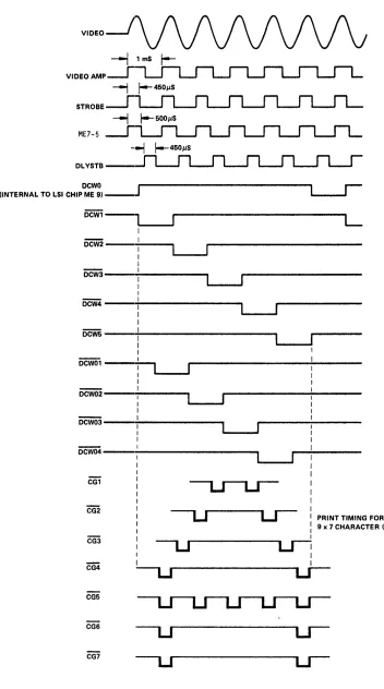
generates the video signal for controlling the print timing. As the print head and optical head assembly moves across tbe timing fence, the vertical slots on the timing fence interrupt light to the optical pick-up head, gen· erating a video signal. The VIDEO AMP output then triggers the STROBE one-shot ME 11 on the logic card, initiating the print timing shown in Figure 4-5.
The STROBE one shot is adjusted for 450 usee. The leading edge of STROBE also triggers a delay one-shot (ME7··12) adjusted for a 500 Llsec output pulse. The trailing edge of this pulse triggers the Delayed Strobe
(Dl YSTB) one-shot which is adjusted to the same pulse width as STROBE. In normal character printing, STROBE is used for Full-Step timing and Dl YSTBfor the Half-Step timing.
Rev. E
4.6.2.1 Video Amplifier
The circuit used to generate and amplify the video signal is located on the video amplifier board attached to the print head carriage.
The video amplifier is comprised of a dual slit sensor and operational amplifier ME 1. Refer to the schematic drawing number 63002669 in Section 7. The dual slit sensor converts light energy monitored throughthe timing fence into electrical energy. As the carriage moves, the light source is interrupted by opaque bars on the timing fence and generates a pulsating output. The positive output generated on each light signal is applied to the postive input of ME
1.
The signal is amplified by ME 1 and provides a high output for each light signal. The duty cycle of VI DEO output is set by adjusting R4.4.6.2.2 Timing Signals
For normal character printing, five consecutive STROBE inputs to LSI chip ME9, generate timing outputs DCW1-DCW5 as shown in Figure 4-4. These timing intervals correspond to the five full-step columns in the character matrix. The quiescent state of this strobe counter is DCWO (internal to the chip) which corresponds to the space interval between characters. During DCWO, the STROBE input gcerates a CLKTB2 pulse which clocks the next character to the output of the shift register. The DCW1-D W5 timing outputs are used to address the appropriate column in the "full-step" ROM (character generator).
During each video interval both a STROBE pulse and () DL YSTB pulse of the same width is generated as shown in Figure 4-4. During normal character printing, four consecutive DL YSTB inputs to LSI chip ME9, generate timing outputs DCW01-DCW04. These four timin9..intervals correspond to the four additional ("half-step") columns in the 9 x 7 matrix. Timing signals (DCW01-DCW04) are used to address the appro-priate column in the "half-step" ROM (character generator).
During elongated character printing, the UCC latch (internal to LSI chip ME9) allows alternate STROBE pulses to clock the internal strobe counter and alternate D L YSTB pulses to clock the delayed strobe counter. As a result, timing outputs DCW1-DCW5 and DCWO 1-DCW04 are twice as long during elongated character mode than during normal character mode.
During the space interval between characters (DCWO), timing signals DCW1-5 and DCW01-04 are all reset.
4.6.3 CHARACTER GENERATOR (ROM)
The logic board can contain up to four ROM elements,. depending on the selected character generating capabilities of that printer. The ROM'S in element locatiomi ME 18 and ME20 each provide full-step outputs (i.e., columns 1,3,5,7,9) for up to 64 characters. The ROM'S in locations ME24 and ME30 each provide half-step outputs (i.e., columns 2,4,6,8) for up to 64 characters.
Each ROM (Character Generator) element had three inputs (in addition to the input voltages):
( 1 )
(2)
(3)
The character address - Outputs TB 1-TB5 from the shift register are buffered and applied to five of the six character inputs to all ROM's. For the full-step and half-step ROM's (ME 18 and ME24), the sixth character address input is controlled by TB6. For ROM's ME20 and ME30, the sixth character address input is controlled~CHADD7. 13y jumper option, CHADD7 can be either TB7 (standard) or TB6 (optional).
Column Address - Timing outputs DCW1-DCW5 from LSI chip ME9 specify the five "full-step" columns in eaeh 9 x 7 character matrix in ROM's ME 18 and ME20. Timing output DCWO; -DCW04 specify the four "half-step" columns in each 9 x 7 matrix in ROM's ME24 and ME30.
Timing - A low input to pin 28 of each ROM gates the 7 - bit dot configuration
VIDEO
VIDEO AMP
ME7-5
DCWO ~---~
r--(IN'rERNAL TO LSI CHIP ME 91 _ _
J
'--_.-I'DCWi-,
' - - - -...
L
~---~
DcW5
----:0---.
PRINT TIMING FOR
9 x 7 CHARACTER (AI
CG5
CG6
[image:28.611.104.456.55.687.2]CG7
Figure 4-4. CHARACTER TIMING
Rev. E
7
r-I N
3C 3C
u u
Cl Cl
r-I
Q
3:
U
Cl
(A)
9
M
3C
u
Cl
N M Q &.
3C 3:
U U
Cl Cl
NORMAL
of the addressed character and column to the output of that ROM. For the full-step ROM's (ME 18 and ME20), this timing input is STROBE AN Ded with ROMTB8 or ROMTB8. By jumper option, ROMTB8 can be ::rO V , +5V, CHADD7, TB8 or TB8, allowing the selected one of these inputs to enable the ROM. The STROBE pulse provides the timing input for gating the 7-bit dot pattern to the print head solenoids.
For the half-step ROM's (ME24 and ME30), the timing input is ROME2 AN Ded with ROMTB8 or ROMTiS8. For normal character printing, ROM E2 generated by LSI chip MEg, is coincident with Delayed Strobe signal DL YSTB. This effectively interleaves the dot pattern from the half-step ROM's with the dot pattern from the full-step ROM's.
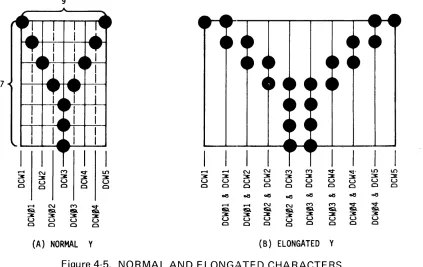
For elongated character printing, ROME2 is coincident with the STROBE sig-nal. This combined with the fact that the DCW timing signals from LSI chip MEg are twice as long during elongated character mode, causes the printed character to be twice as wide as normal characters. An example of the character
(Y), both in normal and elongated style, is shown in Figure 4-5.
c::t U') r-I r-I N N M M c::t 0::1- U') U')
3: 3: 3C 3C 3C 3C 3: 3: 3: 3: 3: 3:
u u u u u u u u u u u u
Cl Cl Cl Cl Cl Cl Cl Cl Cl Cl CI Cl ~ ~ ~ ~ ~ ~ ~
...,
c::t r-I r-I N N M M c::t ¢
Q Q Q Q & Q Q Q Q
3C 3: 3: 3C 3: 3C 3: 3: 3:
U U U U U U U U U
Cl Cl Cl Cl Cl Cl Cl Cl CI
[image:29.611.113.536.256.523.2]Y (B)
ELONGATED
YFigure 4-5. NORMAL AND ELONGATED CHARACTERS
The seven outputs from all four ROM's are wire ORed together and gated out to the Power Driver board as signals CG 1 - CG7. Diodes CR 16-CR32 clamp the ROM outputs to +5V to prevent overloading the inputs to the 74LOO gates. I n normal operation, the STI~OBE or D L YSTB signal gates the addressed dot column to the Power Driver board. The input to ME28 pins. 1 and 2 is normally low holding the output constantly high, enabling the ouptut CG gates. If, however, a failure occurs in the -12V supply, then ME28-1 and 2 goes high forcing ME28-3 low disabling the CG gates.
4.6.4 PRINT HEAD OPERATION
The print head is the device used to do the impact printing of the characters. The head contains seven solenoids that move the tungsten wires against the ribbon to form the column of dots on the paper. The position of these solenoids and the location of the tungsten wires in the head are shown in Section 1. Solenoid No.1 controls the top dot and solenoid No.7 controls the bottom dot in a column. The wires come from each solenoid and are positioned at a jewel located at the end of the head. The length of these wires is approximatllil 3.5 inches and each wire requires about one ounce of force to begin its movement. The amount of force nee;" to move the wires 0.015 inch (i.e., the distance necessary to make a dot on the paper) is about 12 ounces.
The total distance travelled by the wires is approximately 0.015-inch, but under normal operation, the end of the hea? is about
O.OOB
inch from the ribbon and paper. The reason for locating the wires closer than ~.015 Inch from the paper, is to account for the amount of force absorbed by the ribbon and paper upon Impact.The electrical timing and mechanical movement of the wires is shown in Figure 4-6. As shown, a 450 microsecond pulse is used to complete the impact. The voltage used to drive the solenoids is +35 volts unregulated. This voltage is about +35 volts to +38 volts when the pins are in an idle state, but drops to a-bout +30 volts when all pins are engaged at the same time. From the beginning of the 450 microsecond drive pulse, about 200 microseconds is required before the wire starts to move in each solenoid. Once the wire starts moving, an additional 300 microseconds is required before the wire makes an impact on the paper. Approximately 500 microseconds more are required for the wire to retract to its normal position.
~'----1ms
SOLENOI D -,450us DRIVE PULSES
L
I
T
MOTION OF015"
WIRE
' i _
--1275US~
DISCHARGE
OF CURRENT
_~
1 _ _ _ - - - - 'Figure 4-6. PRINT HEAD TIMING
4.6.5 POWER DRIVER CI RCUITS
4.6.5.1 Solenoid Drivers
L
A. Driver Circuit -The wire ORed outputs from the character generator CG1-CG7 are applied to the solenoid power driver circuits where they are inverted, amplified and used to generate current pulses for firing the solenoid in each ,head.
Since all solenoid driver circuits are identical and operate in the same manner, only the first one, controlled by CG 1 will be described.
Referring to Power Driver schematic No. 63002275, when CG 1 goes high indicating an active con-dition for solenoid No.1, current flows through R4. This current flows into the base of 03, turning it on. The current through 03 then develops a positive level across R5. This level causes 02 and 01 to act as emitter followers, developing a voltage of approximately 3.8 volts across R 1. Resistor R2 limits power dissipation in Q2.
Rev. E
The 3.BV across R 1 allows approximately a 2.5 amp current flow through solenoid No.1 and transistor01. When 01 is first turned on, the inductance of the solenoid prevents current flow through 01. Transistor 01 is saturated at this time. VVhen current flow through the solenoid reaches approximately 2.5 amps, 01 goes into the active region and limits the current to this value.
When CG 1 goes inactive low, 03 turns off, turning off 02 and 01. When 01 turns off, the solen-oid current flows through CR2 and C1.The value of C1 is chosen to act as a parallel reasonant circuit with the inductance of the solenoid. Diode CFt2 allows only a quarter-wave of the resonant frequency. A waveform diagram is shown in Figure 4··7.
VOLTAGE
+30V----.
1-CURRENT
0
-Figure 4-7. POWER DRIVER VVAVEFORM
B.
Capacitor Discharge Circuits - After C1, C2, C3, C4, C6, C7 and CB have charged to approximately 60 volts because of the discharging solenoid current, resistors R61, R62, R64, R65, R66 and R67 serve to bleed off this charge so that the capacitors will be at a 30 volt bias at the time of the next discharge. The value of the resistor is chosen so that a time constant of about 275 microseconds results.C. Shut-Off Circuit - Diodes CR39 through CR45 have their cathodes tied together and connected to the collector of 033 and cathode of zener diode CR4B. When the printer is turned on, the +5 volt supply prevents 034 from conducting. This prohibits current from flowing through the voltage divider comprised of resistors R79 and RBO. This prevents 033 from conducting and applies the voltage developed across zener diode CR4B to the cathode of diodes CR39 through CR45. I n this condition diodes CR39 through CR45 cannot shunt current away from the solenoid drivers.
When the printer is shut off, it is characterictic that the 5 volt supply output drops before the 30 volt supply output. When this happens 034 turns on and current flows through the voltage divider comprised of resistors R79 and RBO. 033 is turned on and shunts the zener diode CR4B. This clamps the base of the first emitter follower of each solenoid driver to ground through diodes CR39
through CR45, preventing any of the solenoids from firing during power turn off. The Clutch and Line Feed Drivers are also attached to the collector of 033 through diodes CR36, CR37 and CR38. Therefore, during power turn off, the clutches are released and paper movement is inhibited.
4.6.5.2 Forward Clutch Driver
Power for moving the print head from left to right across the page is transmitte<if!om the main drive motor to an electromechanical clutch mechanism. The clutch is controlled by a low CI P signal from the logic board. This signal is applied via the optional Motor Control board to a driver circuit on the Power Driver card, the output of which activates the clutch.
Signal CI P is normally low thereby causing the current flowing through R42 to be shunted through CR31 ~JroLlnd. Diode CR30 offsets the diode drop of CR31. When signal CIP goes active high, CR31 be-comes back biased, causing current to flow through CR30, R49, and transistor 029, provided that diode CR37 is back biased. This current causes transistors 029 and 028 also flows through and activates the forward clutch. The clutch current is limited by R40.
When CI P goes low, 029 and 028 turn off. Diode CR29 provides a current path until the magnetic field of the forward clutch is dissipated.
4.6.5.3 Reverse Clutch Driver
Power for moving the print head from right to left is transmitted from the main drive motor to a reverse clutch mechanism. Signal CI P from the logic board directly controls the reverse clutch driver on the Power Driver board, unaffected by the optional motor control circuit.
The reverse clutch driver operation is identical to that of the forward clutch driver except that is is controlled by signal CI R instead of CI P.
4.7 PAPER MOVEMENT
Three separate printer functions can cause a paper movement operation: line feed, form feed, and vertical tab. Each of these functions causes the paper to move by activating the Paper Movement Solenoid (PMSO L), which in turn activates a clutch that mechanically links the form feed motor to the paper-feed tractors.
For each line feed operation, the solenoid is energized 15 milliseconds for single line feeds and approx-imately 50 milliseconds for the double line feed opt'ion. At the end of this interval one 60-90 millisecond line feed delay is generated to allow the clutch pawl and clutch mechanism to return home before another paper movement operation is allowed.
In response to a form feed or vp.rtical tab command, a dc level is applied to the solenoid, allowing continuous movement of the paper. This paper movement is terminated when a hole is detected in the appropriate channel of the vertical format paper tape. The operation of the
V
F U is described in Section 4.7.4.To prevent the printer from "hanging up" in a paper movement condition which would waste both time and paper, LSI chip ME5 contains a paper time-out circuit. This circuit is activated by any paper move-ment command. In the standard 101AL printer, the Paper Time-Out (PMTO) interval is factory-adjusted for approximately 6-9 seconds. If, at the end of this time, paper is still advancing, the line feed solenoid command (PMSO L) is immediately deactivated, terminating the paper movement operation, and the FAU L T line to the interface connector is activated.
Rev. E
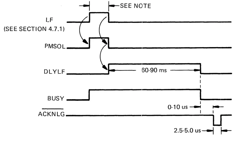
4.7.1 LINE FEED (Figure 4-8)
The line feed operation can be generated by any of the following three conditions:
(1) After printing a line of characters Of the automatic line feed is not disabled, E 1 to E2 is connected) then the low-going forward clutch signal CI P, triggers the LF one-shot.
(2) Receiving a line feed code (octal 012) - LSI chip ME5 decodes the line feed character and generates a 5-10 usee CSLF pulse, the trailing edge of which triggers the LF one-shot.
(3) Pressing the LINE FEED switch on the operator panel - Pressing this switch causes REMLF to go low. This low input to LSI chip ME5 generates a 5-10 usec CSLF pulse, the trailing edge of which triggers the LF one-shot.
The width of the LF pulse generated by any of these three conditions is adjustable. I n the standard 101AL printer, R22 and R23 are not used and jumper E5 to E6 is connected. In this configuration, R19 is adjusted so that a 15 millisecond LF pulse is generated.
LF (SEE SECTION 4.7.1)
~
t--SEE NOTEc::
(I
PMSOL ____
~. ~I~--
__ ____ ____
----DLYLF ______ ...
J:
'60-90 ms---::t~
__ _
BUSY ___ ~
I
0-10us~
...-ACKNLG---I--~LJr__
2.5-5.0 us----l
I--NOTE: 15 MI LLISECONDS FOR SINGLE LINE FEED, [image:33.611.103.505.297.543.2]50 MI LLISECONDS FOR DOUBLE LINE FEED OPTION
Figure 4-8. LINE FEED TIMING
If the double line feed option controlled by an optional switch on the operator panel is used, then jumper E4 to E5 is connected and R22 and R23 are used. VVith the switch in the "double line feed" po-sition, D LF is an open circuit and R 19 has no effect on pulse width. R22 should be adjusted to provide a 50 millisecond LF pulse. When the switch is placed in the "singleline feed" position, DLF goes to +5V, placing R 19 in parallel with R82 and R83. With the switch in this position, R 19 should be adjusted to provide a 15 millisecond LF pulse.
While LF is high, LSI chip ME5 generates a low PMSO [signal which activates the line feed solenoid via the Power Driver board. The trailing edge of PMSOL tri~lgers the 60-90 millisecond Delay Line Feed interval DL YLF. During both the LF and DL YLF intervals, the printer remains busy.
4.7.2 FORM FEED (Figure 4-9)
A form feed operation can be generated by either of the fol/owing two conditions:
(1) Receiving a form feed code (octal 014) - LSI chip ME5 decodes the form feed character and generates a I'ow PMSOL signal to activate the line feed solenoid. If the DSC option is used (E10-E11), the line is printed before PMSOL is ac-tivated.
(2) Pressing the TOP OF FOHM switch on the operator panel - This generates a low TOFSW signal causing LSI chip ME9 to generate a low PMSOL signal.
The low PMSO L signal activates the I ine feed solenoid and generates a busy condition. Th is con-tinues until a hole is detected in ch~nel 7 of the paper tape. This generates a high F F H input to LSI chip ME5, which deactivates PMSOL.
For as
1075
as PMSO L is active, the printer remains in a busy condition. I f a paper time-out is detected, PMS L is immediately deactivated and the FAU L T line is activated.4.7.3 VERTICAL TAB (Figure 4-9)
A vertical tab operation is generated by receivin~a vertical tab code (octal 013). LSI chip ME5 de-codes the vertical tab character and generates a low PSO L signal. I f the DSC option is used (E 1 O-E 11 ), the line is printed before PMSO L is activated.
The low PMSO L signal initiates the paper movament and generates a busy condition. This continues until a hole is detected in channel 5 of the paper tape. This generates a high F F H input to LSI chip ME5, wh ich deactivates PMSO L.
For as long as PMSO L is active, the printer remains in a busy condition.
FORM FEED OR VERTICAL TAB (SE E SECTIONS 4.7.2 & 4.7.3)
PMSOL
F F H OR VTH ---~r__--..
DL YLF _ _ _ _ _ _ _ _ _ ...
1==
60-90 ms:::t .. __
BUSY _ _ ....
ACKNLG
L
I I
0-10 us ~ t---I I
LJ
2.5-5.0, us
---I
r--Figure 4-9. FORM FEED AND VERTICAL TAB TIMING
Rev. E
4.7.4 VERTICAL FORMAT UNIT
The vertical format unit (VFU) consists of a standard 8-channel paper tape reader, located on the upper left side of the printer. Movement of the paper tape in the VFU is caused by direct mechanical linkage to the gear train that drives the paper feed tractors. As a result, each line feed advances the paper by one line and the tape by one sprocket hole.
Each form feed function advances paper until the next hole is detected in channel 7 of the paper tape. Similarly, each vertical tab function advances paper until the next hole is sensed in channel 5 of the paper tape. A schematic of the VFUamplifier is shown in Figure 4-10.
r";P'ERSEcnoN---,
I
I
I
L _ _ _ _ _ _ ~
~----
-1
I
I LOWER
I
SECTION--+----b
I
ME1l8TI-I
I I
I
I
I
I
ME 118~
L
_____
.JI
I
25C4580
Q2
2SC4580
01
L _ _ _ _ _ _ _ _ _ _
J
J120
Pll9 +5 VDC
CHANNEL 7 1
CHANNEL 5
LINE FEED
r - - - I 8
LF RET SPARE
- - 5
SPARE SPARE
Figure 4-10. VFU TAPE READER AMPLIFIER (LOCATED IN VFU)
Holes detected in Channel 5 or 7 of the tape are amplified by a VFU amplifier contained in the tape reader unit. Each channel in the vertical format contrOiI tape reader contains an input photo transis-tor, driving an emitter follower amplifier. When the photo transistor receives light, current flows through it and into the base of the emitter follower generating a +5\1 output. The two amplifier outputs CHANNE L 5 and CHANNEL 7 are then applied to the logic board and ME25 as VTH and FFH. A 2-4 millisecond delay is designed into ME25 for noise immunity.
4.7.5 LINE FEED SOLENOID DRIVER
Logic signal PMSOL from LSI chip ME5 is buffered by ME10 to generate PMSOL to the Power Driver board. (Schematic No. 63002275).
Signal PMSO L is normally low (inactive). I n this state, current flows through R39 and CR28 to ground. The diode drop of CR27 balances the diode drop of CR28 thereby maintaining the line feed driver in the off condition.
When PMSOL goes active high, CR28 becomes back biased and current flows through R39, CR27, R48 and into the base of 027, saturating it. The collector Gurrent, limited by R38, flows into tra"nsistor 026, turning is on and causing current to flow through the Line Feed Solenoid. When signal PMSOL re-turns low, transistors 027 and 026 turn off. The fly-back voltage then appears across CR24, which pro-vides a current path until the magnetic field of the line feed solenoid is dissipated.