I
I
I
I
[
[
[
[
I
[
[
I
[
[
[
[
[
I
I
CIP/2100 PRELIMINARY
REFERENCE MANUAL
September, 1969
INFORMATION PRODUCTS GROUP CIMTROL DIVISION
[
[
[
[
[
[
[
[
[
[
[
[
[
[
I
I
1.
2.
3.
4.
TABLE OF CONTENTS
SYSTEM DESIGN FEATURE
1
General Characteristics
1
SYSTEM ORGANIZATION
3
Registers
3
Core Memory
.
4Interrupts 4
Internal Interrupts 4
External Interrupts
5
Information Format
5
Data Format
5
Address Word Format
6
Instruction Format
6
Operand Addressing Modes
6
INSTRUCTION REPERTOIRE 11
Control 11
Conditional Jumps 14
Shifts
15
Register Operate
19
Memory Reference
23
INPUT/OUTPUT OPERATIONS
30
Serial Input/Output Instructions
30
Byte Input/Output Instructions
31
Device Address
31
Device Orders .
32
Status Bytes
32
Instruction
33
Concurrent Input/Output
35
Address Control
35
Concurrent Operations
36
[
[
[
[
(
[
[
[
[
[
[
[
[
I
I
A.
B.
C.
D.
E.
F.
G.
1.
2.
3.
APPENDIXES
CIP/2000 File Register Assignments
Dedicated Memory
Execution Times
Standard Character Codes
[image:3.612.67.545.56.714.2]Teletype Control Codes
Table of Powers of Two
Hexadecimal - Decimal Integer Conversion Tables
TABLES
Effective Address Computation
Device Orders . . . .
Status Bytes Definition . . . .
37
38
39
41
42
43
44
10
32
32
I
[
I
[
I
[
I
I
[
[
1.
SYSTEM DESIGN FEATURES
The CIP/2IOO is a microprogrammed configuration of the CIP/2100 hardware. The CIP/2000 is a microprogrammed, byte oriented computer system designed for general purpose and dedicated system applications. The functional, mechanical, and electrical design is the basis for a series of machine configurations built with standard functional blocks. The CIP /2100 microprogram (firmware) converts the CIP /2000 system into a software programmable computer with a general-purpose instruction repertoire, I/O facility, and option features.
The design concepts embodied in the CIP/2100 provide a unique combination of features unavailable in other small computer systems. These include:
Speed
The machine incorporates 220 nanosecond micro command execution and a 1.1 microsecond core memory cycle time. The short micro command clock step and core memory cycles allow for fast execution of the exceptionally powerful CIP /2100 instructions, high input/output transfer rates, and excellent overall through-put rates.
Flexibility
Microprogramming permits tailoring of the system to specific applications. Application-oriented macro instructions or microprogrammed subroutines may be added to the standard CIP/2IOO instruction repertoire to increase system efficiency and through-put and to reduce hardware costs. The modular design of the core memory, read only store, processor options, and input/output elements permits expansion of the basic system as required. The compact 8-3/4 inch high enclosure has a number of spare circuit board slots and ample power for system and peripheral interface even when the computer is fully expanded.
Low System Cost
The CIP/2IOO uses TTL monolithic integrated circuits, including a large number of the medium scale integration types, for savings in parts and assembly time. The use of read only storage for control further reduces the number of circuits that might otherwise be required to provide the same functional capability. The packaging and powering of the CIP/2000 has been designed for system applications rather than stand-alone computer operation to reduce integration costs to a minimum. The higher microcommand execution speed can be used to minimize interface and controller hardware, resulting in further reduction of system cost.
GENERAL CHARACTERISTICS
The advance features and operating characteristics of the CIP/21 00 include:
Memory addressing to 32K
4096 byte plug-in memory modules
16K of memory in basic 8-3/4 inch enclosure 1.1 microsecond full memory cycle time
-I
I
[
[
I
[
I
I
I
[
[
[
I
I:
I
[
I
I
I
Direct memory access option Six operational registers
Accumulator (A) - 16 bits
Auxiliary accumulator (B) - 16 bits Index register (X) - 16 bits
Program counter (P) - 15 bits Overflow (0) - 1 bit
Word length control (W) - 2 bits
Extensive, powerful instruction set including 89 individual operations: Multiply and divide (2)
Control (1 7)
Multi-bit arithmetic and logical shifts (12) Conditional jumps (16)
Input/Output (8) Inter-register (16)
Memory reference including jump, compare and variable word length operations (18)
Eight operand addressing modes including: Direct to page 0 (first 256 bytes)
Direct relative to P (± 128 bytes)
Indirect to page 0 (first 256 bytes)
Indirect relative to P (± 128 bytes)
Indexed (to 32,768 bytes)
Indexed with bias (to 32,768 bytes) Extended address (to 32,768 bytes) Literal
Multi-precision 1,2,3, or 4 byte load, store, and arithmetic operations Flexible I/O facilities including:
programmed transfers to/from A and B registers and memory concurrent buffered I/O
direct memory access
Expandable priority interrupt system Processor options which include:
real-time clock
power-fail detect and automatic restart memory parity detect and interrupt memory page protect
Built-in bootstrap loader in non-volatile read only store Basic software including:
loader
teletype debug and operating system two-pass assembler
diagnostics
TTL integrated circuitry
Power: 115/230 vac, 50-60 cycle, 380 watts
Environment: 0-500C
Dimensions: 8-3/4 inches high, 19 inches wide, 23 inches deep
~~"., .. ,~ ... ,~ ."----~.,---...
-I
[
[
I
[
[
[
[
I
I
[
I
I
I
I
[
[
I
I
2. SYSTEM ORGANIZATION
The basic elements of the CIP/2100 include the operational registers, core memory, interrupt system, input/output system, and control console. A group of processor options is also available to meet a broad range of special system requirements.
REGISTERS
The CIP /2100 contains six operational registers which are accessible to the programmer. These operational registers occupy nine of the sixteen file registers of the basic CIP/2000 hardware; the remaining seven hardware registers are not accessible by the CIP/2100 instructions although specially designed macros could make use of these at the micro-level. The assignment of the file registers is given in Appendix A.
A Register
The 16-bit A register is the accumulator with which most operations are performed. The A register holds the upper portion of 24-or 32-bit data words and all of 8-and 16-bit data words. The A register may be shifted by itself or in conjunction with the B register.
B Register
The 16-bit B register is the auxiliary accumulator and is used mainly as an extension of the accumulator to hold the lower 16 bits of 24-and 32-bit data. The B register may be shifted by itself or in conjunction with the A register.
X Register
The 16-bit X register is an index register used in address modification. It can communicate
directly with memory, be incremented, and compared with the A register.
P Register
The IS-bit P register is the program counter which holds the address of next memory instruction to be executed.
W Register
The 2-bit W register holds the word length mode. It is loaded by a control instruction and
sets the byte length of the operand for all variable word length instructions.
o
RegisterThe one-bit 0 register holds the overflow flag. The overflow is set by arithmetic instructions
when an overflow occurs, by execution of a Control instruction, or by the Compare
instruction. It may be reset by execution of a Control instruction or by a Conditional Jump
instruction that tests for an overflow condition.
I
I
[
[
[
[
[
I
11
Il
I
I
[
[
I
[
[
I
I
CORE MEMORY
The magnetic core memory is organized into pluggable modules of 4096 bytes. The memory is byte addressable. Each byte contains eight information bits and an optional memory parity bit. A spare memory bit is also available for special applications.
The memory may be expanded up to four modules (16,384 bytes) within the basic 8-3/4 inch cabinet. Memory addressing is available to 32,768 bytes. The memory cycle time is 1.1 microseconds.
A memory protect option provides a guarantee that protected areas of memory cannot be written into by a program residing in unprotected memory or by unprotected peripheral devices. The memory is divided into a maximum of 32 protected areas.
The direct memory access (DMA) option allows for interfacing peripheral devices directly with the memory to provide peak transfer rates of up to 910,000 bytes per second.
INTERRUPTS
The CIP/2100 priority interrupt system provides for internal processor interrupts, I/O peripheral device interrupts, and groups of individual external interrupts, each with its own unique interrupt memory address and priority assignment.
INTERNAL INTERRUPTS
Internal interrupts include those that are supplied as part of the basic CIP/2100 system as well as optional features. The internal interrupts have priority over external interrupts. The internal interrupts are listed below in order of their priority.
Console
The standard console interrupt is triggered by a switch on the console, allowing an operator to exert control. This interrupt routine is also used by the trap instruction.
Real-Time Clock
The optional real-time clock interrupt occurs when a preset clock count in a unique memory location is incremented to zero. The clock count location is automatically advanced at each clock time. The real-time clock interrupt is enabled and disabled under program control.
Memory Protect
The optional memory protect interrupt occurs when an illegal write operation has been attempted in a protected area of memory.
Memory Parity
The optional memory parity interrupt occurs when a byte parity error is detected when reading from a memory location.
Memory Boundary
The optional memory boundary interrupt occurs when a non-existing memory location is addressed.
~---,_.~ __ ,,," >'.' •. "·"~"".,_",""'.M __ ".'""'.' •• '._" _ _ _ _ _ _ _ _
I
I
[
I
I
[
[
[
[
I
[
(
I(
I![
i(
I
I
Power-Fail
The optional power-fail interrupt provides an interrupt when a loss of primary power is detected. A minimum of two milliseconds of computer operation are assured after the interrupt.
Power-On
The optional power-on interrupt occurs when the power is applied and is up to normal operating levels.
EXTERNAL INTERRUPTS
External interrupts may be associated with peripheral devices or may be individual lines not
associated with devices on the 1/0 bus. The device interrupts are used to indicate such
conditions as ready, error, and end of operation conditions in the device. These interrupts are enabled by function code to the device controllers. The memory location containing the interrupt routine address is 1 00 16 plus twice the Device Address.
Individual interrupts are handled by an external interrupt module which provides for arming/disarming individual interrupts and enabling/disabling recognition of interrupts in the group. Standard external interrupt cards containing 8 priority interrupt lines are avaliable. A total of 64 external interrupts can be implemented.
INFORMATION FORMATS
The basic element of information is an 8-bit byte in which the bit positions are numbered from 7 through 0, left to right. Both instructions and data occupy a variable number of bytes for maximum storage efficiency. A word is a 16-bit element of information consisting of two bytes. The accumulator and index register both hold a 16-bit word.
DATA FORMAT
Data in the CIP/2100 is variable precision of 8, 16, 24, or 32-bit length. Negative numbers are represented in 2's complement form. The range of magnitude and data format in the A and B registers for the four data lengths is shown below:
8 Bits (1 Byte)
Sign Extend ± Magnitude (unused)
,. ,.
13 12 I 11 10 9 8 1 6 5 • I 3 2 1 0" " 13 12 111 10 9 8 I 1 6
•
• I 3 2 1 0A Register B Register
16 Bits (2 Bytes) Range: +2 15_1 to _2 15
+ Magnitude (unused)
•
,.
13 12 I 11 10 9 8 I 1 6•
• I 3 2 1 0 15,.
13 12 I 11 10 9 8 I 1 6•
• I 3 2 1 0A Register B Register
I
I
[
I
I
[
[
I
[
[
[
[
[
[
'I
24 Bits (3 Bytes) Range· +223_1 to _223
Sign Extend
±
Magnitude15 I. 13 12 I 11 10 9 8 7 6 5 • I 3 2 1 o I 15
" 13 12 I 11 10 9 8 I 7 6 5 • I 3 2 1 0
A Register B Register
32 Bits (4 Bytes) Range: +231 _1 to _231
Magnitude
15 I. 13 12 I 11 10 9 8 I 7 6 5 • I 3 2 1 0 I 15 I. 13 12 I 11 10 9 8 I 7 6 5 • I 3 2 1 0
A Register B Register
ADDRESS WORD FORMAT
A 16-bit address word contains a IS-bit memory address and an index flag as shown below. The address may be a direct or indirect address as dictated by the instruction operation code. The value of the address word is equal to the contents of bits 14-0 and is equal to the contents of bits 14-0 plus the contents of the x register if bit 15 is a I-bit.
IJ "
"I~
...J
z6 5 • I 3 2 1 0
INSTRUCTION FORMAT
Instruction formats are one to five bytes, but in all cases the first contains an eight-bit operation code which defines the operation class, the sub-operation code, and any modifiers. Succeeding byte(s} contain such information as:
Single byte absolute or relative address Double byte address word
Single byte shift count
Single byte I/O function and device address I, 2, 3, or 4 byte literal data.
OPERAND ADDRESSING MODES
The memory reference instructions defined in the following section each have eight possible modes of addressing an operand in memory. The number of bytes in the instruction format varies with the mode. The additional bytes of the instruction contain addresses, partial addresses, or data (literals).
The basic memory reference instruction is one byte containing two fields as follows:
DPCode I m 1
7 6 5 4 1 3 2 1 0
The S-bit operation code defines the basic instructions; the 3-bit m field specifies the address mode. Additional bytes contain the address of an operand, an indirect address, a base address, or a literal depending upon the addressing mode. The effective operand address is the memory location specified after all indirect and/or index modifications have been performed.
I
[
[
I
[
[
[
[
[
[
[
I:
[
[
[
I
[
I
I
When an indirect address mode is specified, the location of the indirect address word is the first byte of a two-byte word having the format shown below:
Ix!
v
J
z4
I
3 4I
37 6 5 2 1 6 5 2 1 0
Indirect Address Word Format
Bit 7 of the first byte (x) defines whether or not the indirect address word will be modified by the contents of the index register:
If x
=
0, the IS-bit number formed by y and z is the effective operand address.If x = I, the IS-bit number formed by y and z is a base address to which is added the
contents of the X register. The result is the effective operand address.
The individual addressing modes and the memory reference instruction format for that mode are defined below.
DIRECT PAGE 0 (m=O)
v
6 5 4 I 3 2 1 0
The effective operand address is given by the contents of the second byte of the instruction (y) with seven high order zero bits appended. This mode provides direct addressing of operands in the first 2S6 memory locations.
DIRECT RELATIVE (m=1)
I
OP CodeI
7 6 5 4 1 3 2
J
6 5 4 I 3 2 1 0v
The effective operand address is given by the sum of the contents of the second byte (y) with its high order sign bit (bit 7) extended and the contents of the P register. The contents of the P register at the time the addition is performed is the address of the memory location following y. This mode provides for addressing from 127 locations ahead to 128 locations behind the memory location of the next instruction.
I
[
I
I
(
[
[
I
I
I
[
[
[
[
[
[
II
I
INDIRECT PAGE 0 (m=2)
v
6 5
• I
3 2 1 0An indirect address word is specified by the contents of the second byte (y) of the instruction with seven high order zero bits appended. The 2-byte indirect address word addressed is located in the first 256 memory locations. The effective operand address is given by the contents of the indirect address word if the index flag (bit 15) is an O-bit, or by the sum of the contents of the indirect address word and the X register if the index flag (bit 15) is a I-bit.
INDIRECT RELATIVE (m=3)
v
6 5
• I
3 2 1 0
An indirect address word is specified by the sum of the contents of the second byte (y) with its high order bit (bit 7) extended and the contents of the P register. The contents of the P register at the time the addition is performed is the address of the memory location following y. The effective operand address is given by the contents of indirect address word if the index flag (bit 15) is an O-bit or by the sum of the contents of the indirect address word and the X register if the index flag (bit 15) is a I-bit.
INDEXED (m=4)
OP Code 4
7 6 5 4 1 3 2 1 0
The effective operand address is given by the contents of the X register.
INDEXED WITH BIAS (m==5)
v
6 5
• I
3 2 1 0, .~ •. ~~~.".~ .. _ •• ·"",~U~ ___
I
[
[
[
(
[
[
[
I
I
' I[
i[
[
I
[
I
[
I
I
The effective operand address is given by the sum of the contents of the X register and the contents of the second byte (y) of the instruction.
EXTENDED ADDRESS (m=6)
I,
~p ~~.J
6 •H
.
J
y Z
4
I
3 2 , 0• I
3 2 , 6 5A 16-bit address word is located in the second and third byte of the instruction. The effective operand address is given by the contents of the address word if the index flag bit in bit 15 is an O-bit, or by the sum of the contents of the address word and the X register if the index flag is a I-bit.
LITERAL (m=7)
Operand 1-4 Byte Operand
5 4 I 3 2 , 0 7 6 5 4 I 3 2 , 0
The effective operamJ address is given by the contents of the P register. The operand is located in from 1-4 bytes following the first byte of the instruction, depending upon the operand precision. The P register is incremented for each operand byte accessed. The Jump and Return Jump memory referencing instructions do not have a literal mode.
JUMP/RETURN JUMP INDIRECT EXTENDED ADDRESS (m=7)
I ,
~p ~'J
7.1:1.
J
y
• I
3z
• I
32 , 6 5 2 , 0
A 16-bit direct address word is located in the second and third bytes of the instruction. This word addresses an indirect address word located at the address given by the contents of the second and third bytes if bit 15 of the address word is an O-bit or by the sum of the contents of the second and third bytes and the X register if the index flag bit in bit 15 is a
I-bit.
The effective jump address is given by the contents of the indirect address word if the index flag in bit 15 of the indirect address word is an O-bit, or by the sum of the contents of the indirect word and the X register if the index flag bit in bit 15 of the indirect address word is a I-bit.
I
I
[
I
MI
0[
2 1[
34
[
56
[
7I
7I
[
I
[
[
I
I
I
I
TABLE 1. EFFECTIVE ADDRESS COMPUTATION
Effective Address
X= 0:
X = 1:
X=O:
X = 1:
Iyl
y
+
(P)(I
yI)
(y+ (P))
(X)
Iyl
+
(X) y,z y,z + (X) (P)(y,z) (y,z + (X))
Mode
Direct Page 0
Direct Relative
Indirect Page 0
Indirect Relative
Indexed
Indexed with Bias
Extended Address
Extended Address Indexed
Literal
I ndirect Extended Address (Jump and Return Jump only) Indirect Extended Address Indexed
(Jump and Return Jump only)
[image:13.612.119.561.146.433.2]I
[
I
I
[
I
I
[
[
[
[
[
[
[
I
I
I
3. INSTRUCTION REPERTOIRE
This section contains descriptions of all CIP/2l00 instructions except input/output. The latter class is described in Section 4. With each description is a diagram showing the format of the instruction and its operation code, normally given in hexadecimal. Above each diagram are the mnemonic code and the name of the instruction. Under each diagram is a description of the instruction, followed by a list of the registers and indicators that can be affected by the instruction. The timing of each instruction is given in Appendix C.
CONTROL
The control group of instructions. are single byte instructions which provide specific control functions.
HLT
HALT
00
7 6 5 4
I
3 1 1 0The processor and concurrent I/O are halted. The contents of the P register will be the address of the halt instruction plus one. Depressing the console run or step switches will cause the next instruction to be executed.
TRP
TRAP
01
7 6 5 4 I 3 1 1 0
The contents of the P register are stored at the two-byte memory location specified by the two-byte address word at location 8016. Subsequently, the two-byte address word (at 8016) plus two replaces the original contents of the P register. Execution of this instruction is the same as depressing the console interrupt switch. Interrupts are not recognized before the execution of the next instruction.
Affected: P, Memory.
I
[
[
[
I
I
I
[
[
[
[
[
I
I
I
ESW ENTER SENSE SWITCHES
7 6 5
02
4 I 3 2 1 0
The status of the four console sense switches is placed in bits 15-12 of the A register. If the
sense switch is on the corresponding bit in the A register will be set to one. Bits 8-11 of the A register are set to one and bits 0-7 are unaltered.
Affected: A
PMP PROTECT MEMORY PAGE
03
7 6 5 4
I
3 2 1 0This instruction causes the memory protection status for an area of memory to be updated if the memory protect option is implemented. Only a single 256, 512, or 1024 word area is affected. The 5, 6, or 7 high order bits of the memory address must be in the low order bits of the A register and the protect state must be in bit 15 of the B register. A one in the high order bit of B sets the area to the protected state; a zero sets it to the unprotected state. The contents of the A and B registers are not affected.
DIN DISABLE INTERRUPT SYSTEM
04
7 6 5 4 I 3 2 1 0
All external interrupts are disabled, preventing the processor from recongnizing an external interrupt request. Interrupts are saved in the disabled state.
I
I
I
I
I
[
[
(
[
I
(
I
[
[
I
I
I
I
EIN ENABLE INTERRUPT SYSTEM
7 6 5 05
• I
3 2 1 0All external interrupts are enabled, allowing the processor to recognize an external interrupt. An interrupt request is serviced after the current instruction is executed.
DRT DISABLE REAL TIME CLOCK
7 6 5 06
4 I 3 2 1 0
The updating of the real-time clock memory location and the generation of real-time clock interrupts are inhibited if the real-time clock is implemented.
ERT ENABLE REAL TIME CLOCK
07
7 6 5 4 I 3 2 1 n
The updating of the real-time clock memory location and the generation of real-time clock interrupts are enabled if the real-time clock is implemented.
RESET OVERFLOW AND SET WORD LENGTH
OP Code
7 6 5 4 1 3 2 1 a
The Overflow register is reset and the variable precision mode (byte length) is placed in the W register. The four instructions are as follows:
OP Code
08
09
Mnemonic
R01 R02
Instructions
RESET OVERFLOW AND SET WORD LENGTH TO 1 RESET OVE RF LOW AND SET WORD LENGTH TO 2
I
I
[
I
I
[
[
(
[
[
[
I:
[
[
[
[
[
I
I
OP Code Mnemonic
OA R03
OB R04
Affected: 0, W
Instructions
RESET OVERFLOW AND SET WORD LENGTH TO 3
RESET OVERFLOW AND SET WORD LENGTH TO 4
SET OVERFLOW AND SET WORD LENGTH
OP Code
7 6 5 4 I 3 2 1 0
The overflow register is set to One and the variable precision mode (byte length) is placed in
the W register. The four instructions are as follows:
OP Code Mnemonic
o
C SOlo
D S02o
E S03OF S04
Affected: 0, W
NOP NO OPERATION
7 6 5
34
4 I 3 2 1 0
Instructions
- SET OVERFLOW AND SET WORD LENGTH TO 1
- SET OVERFLOW AND SET WORD LENGTH TO 2
- SET OVERFLOW AND SET WORD LENGTH TO 3
- SET OVERFLOW AND SET WORD LENGTH TO 4
This instruction performs no operation.
CONDITIONAL JUMPS
OP Code
J
y7 6 5 4
I
3 2 6 5 4I
3 2 1 0The conditional jump instructions are a two byte format. The first byte provides the
operation code which includes the condition being tested (bits 2-0) and whether the jump
will be made on the condition being true or false (bit 3). The second byte contains an 8-bit signed value, y, which specifies a jump location relative to P.
I
I
I
I
[
[
[
[
[
[
[
[
I
[
I
[
I
I
If the test condition is met, the sum of the contents of the second byte (y) with its high order bit extended and the current contents of the P register is placed in the P register; otherwise the P register remains unaltered and the next instruction in sequence is accessed. The contents of the P register at this time is the address of the next instruction. The instructions which test the overflow condition also reset the overflow register.
The conditional jump instructions, their operation codes and mnemonics follow:
OP Code Mnemonic Instructions
10 JOV JUMP F OVERFLOW SET
1 1 JAZ JUMP F A EQUAL TO ZERO
1 2 JBZ JUMP F B EQUAL TO ZERO
1 3 JXZ JUMP F X EQUAL TO ZERO
1 4 JAN JUMP F A NEGATIVE
1 5 JXN JUMP F X NEGATIVE
1 6 JAB JUMP F A EQUALS B
1 7 JAX JUMP F A EQUALS X
1 8 NOV JUMP F OVERFLOW NOT SET
1 9 NAZ JUMP F A NOT EQUAL TO ZERO
1 A NBZ JUMP F B NOT EQUAL TO ZERO
1 B NXZ JUMP F X NOT EQUAL TO ZERO
1 C NAN JUMP F A NOT NEGATIVE
1 0 NXN JUMP F X NOT NEGATIVE
1 E NAB JUMP F A NOT EQUAL TO B
1 F NAX JUMP F A NOT EQUAL TO X
Affected: P,O
SHIFTS
The shift group of instructions provides both arithmetic and logic shifts of A register, B register and A and B registers together. A signed shift count is specified in the second byte of the instruction. The shift count is any positive number from 0 to 127; if negative a no operation results. A concurrent input/output request is acknowledged between bit shifts of all shift instructions.
LLA LOGICAL LEFT A
7 • 5
20
4
I
3 , 1J
n
• 5 4 I 3 , 1 0
The contents of the A register are shifted n bits to the left. Bits shifted out of A 15 are shifted into AO
Affected: A
I
I
[
I
(
[
I
(
I
I:
[
[
I
[
[
[
I
I
~ .. ~.-.. ~ .. ~-~-..
_._--._---_._--LLB LOGICAL LEFT B
21
J
6 5n
4
I
3 2 1 0 7 6 5 4I
3 2 1The contents of the B register are shifted n bits to the left. Bits shifted out of B 15 are shifted into BO.
Affected: B
LLL LOGICAL LEFT LONG
22
J
n7 6 5 4
I
3 2 1 6 5 4I
3 2 1 0The contents of the A and B registers are shifted n bits to the left. Bit shifted out of A IS are shifted into BO. Bits shifted out of B IS are shifted into AO.
Affected: A, B
LRA LOGICAL RIGHT A
24
J
n7 6 5 4
I
3 2 1 6 5 4I
3 2 1 0The contents of the A register are shifted n bits to the right. Zeros are shifted into A IS, and bits shifted out of AO are lost.
Affected: A
LRB LOGICAL RIGHT B
25
J
6 5n
4
I
3 2 1 0 7 6 5• I
3 2 1-~-~-~,."'-... -.. --.-~.~.~. ---"--'---"-~ .. -"-'---~"-'~'''~-
.'~-.'~".'~"~"'.'~"-"-'-'--"'"---'----'.-.---.---_._._-I
I
I
I
[
[
I·
, I[
[
[
I
[
[
[
I
I
I
I
The contents of the B register are shifted n bits to the right. Zeros are shifted into B 15, and bits shifted out of BO are lost.
Affected: B
LRL LOGtcAL RIGHT LONG
26
J
n7 6 5 • I 3 2 1 6 5
• I
3 2 1 0The contents of the A and B registers are shifted n bits to the right. Zeros are shifted into AIS. Bits shifted out of AO are shifted into BlS, and bits shifted out of BO are lost.
Affected: A, B
ALA ARITHMETIC LEFT A
7 6 5
28
• I
3 2 1J
6 5n
• I
3 2 1 0The contents of the A register are shifted n bits to the left. Bits shifted out of A 15 are lost. Zeros are shifted into AO.
Affected: A
ALB ARITHMETIC LEFT B
2 1 0
The contents of the B register are shifted n bits to the left. Bits shifted out of B 15 are lost. Zeros are shifted into BO'
Affected: B
I
I
I
[
I
I
[
I
I
I
[
I
I
I
I
I
I
ALL ARITHMETIC LEFT LONG
2A
I
n1 0
The contents of the A and B register are shifted n bits to the left. Bits shifted out of A 15 are lost. Bits shifted out of B 15 are shifted into AO. Zeros are shifted into BO.
Affected: A, B
ARA ARITHMETIC RIGHT A
2 C
I
n6 5 4 1 3 2 1 0 7 6 5 4 1 3 2 1 0
The contents of the A register are shifted n bits to the right. The sign bit in A 15 is copied into vacated high order bits. Bits shifted out of AO are lost.
Affected: A
ARB ARITHMETIC RIGHT B
20
I
n2 1 0
The contents of the B register are shifted n bits to the right. The sign bit in B 15 is copied into vacated high order bits. Bits shifted out of BO are lost.
Affected: B
ARL ARITHMETIC RIGHT LONG
, 6 5
2 E
4
I
3 2 1J
n
6 5 4
I
3 2 1 0I
I
I
I
[
I
I
[
I
[
[
[
[
I
[
I
I
The contents of the A and B registers are shifted n bits to the right. The sign bit in A 15 is copied into vacated high order bits. Bits shifted out of AO are shifted into B 15, and bits shifted out of BO are lost.
Affected: A, B
REGISTER OPERATE
The register operate group of instructions provides for special arithemtic and logical operations on individual registers and between registers. All instructions of this group are a single byte in length.
ORA
I
OR BWITH A
7 6 5
40
4
I
3 2 1 0The logical inclusive-OR of the contents of the A register and the contents of the B register is placed in the A register.
Affected: A
XRA EXCLUSIVE-OR B WITH A
7 6 5
41
4 I 3 2 1 0
The logical exclusive-OR of the contents of the A register and the contents of the B register is placed in the A register.
Affected: A
ORB OR A WITH B
7 • 5
42
4
I
3 2 1 0I
I
[
[
I
(
I
I
[
[
[
I
(
[
[
I
I
The logical inclusive-OR of the contents of the A register and the contents of the B register is placed in the B register.
Affected: B
XRB EXCLUSIVE-OR A WITH B
1 6 5
43
4
I
3 2 1 0The logical exclusive-OR of the contents of the A register and the contents of the B register is placed in the B register.
Affected: B
INX INCREMENT X
1 6 5
44
4
I
3 2 1 0The contents of the X register plus one replaces the contents of the X register. If the result
is greater than 215_1, the overflow register is set.
Affected: X, 0
DCX DECREMENT X
45
1 6 5 4
I
3 2 1 0The contents pf the X register minus one replaces the contents of the X register. If the result
is less than -2 5, the overflow register is set.
Affected: X, 0
I
I
I
r
[
(
[
[
[
[
I
I
[
(
[
I
[
I
I
AWX ADD WORD LENGTH TO X
46
7 6 • 4
I
3 2 , 0The contents of the W register is added to the c?ntents of the X register and the sum is placed in the X register. If the sum is greater than 2 5-1 the overflow register is set.
Affected: X, 0
SWX SUBTRACT WORD LENGTH FROM X
7 6 •
47
4
I
3 2 , 0The contents of the W register is subtracted from the contents of the X register and the difference is placed in the X register. If the difference is less than -2 5, the overflow register is set.
Affected: X, 0
INA INCREMENT A
48
7 6 • 4
I
3 2 , 0The contents pf the A register plus one replaces the contents of the A register. If the sum is
greater than 2 5-1, the overflow register is set.
Affected: A, 0
INB INCREMENT B
7 6 •
49
4
I
3 2 , 0I
[
I
[
I
I
[
(
[
,I ,
[
[
[
[
[
[
I
I
I
The contents
Ys
the B register plus one replaces the contents of the B register. If the sum isgreater than 2 -1, the overflow register is set.
Affected: B, 0
OCA ONE'S COMPLEMENT A
4A
7 6 5 4
I
3 2 1 0The one's complement of the contents of the A register replaces the contents of the A register.
Affected: A
OCB ONE'S COMPLEMENT B
7 6 5
4B
4
I
3 2 1 0The one's complement of the contents of the B register replaces the contents of the B register.
Affected: B
TAX TRANSFER A TO X
7 6 5
4C
4 I 3 2 1 0
The contents of the A register are placed in the X register.
Affected: X
!
I
I
(
I
[
I
[
[
[
[
[
[
[
I
I
'I
II
TBX TRANSFER B TO X
7 6 5
4D
4
I
3 2 1 0The contents of the B register are placed in the X register.
Affected: X
TXA TRANSFER X TO A
7 6 5
4E
4 I 3 2 , 0
The contents of the X register is placed in the A register.
Affected: A
TXB TRANSFER X TO B
7 6 5
4F
4
I
3 2 1 0The contents of the X register is placed in the B register.
Affected: B
MEMORY REFERENCE
The 20 instructions of the memory reference group obtain their operands from memory. The operand memory location is addressed by one of eight modes as explained in section 2. The number of bytes required for the instruction depends on the addressing mode and for the literal mode, the length of the operand.
In the following instruction descriptions only the first byte of the instruction which
contains the basic operation code and the addressing mode is shown. The two-digit
hexadecimal code given is for an operand addressing mode of 0 (m
=
0). For anotherI
I
I
I
(
I
[
I:
I
[
[
[
[
I
[
I
I
I
addressing mode, the value of m must be added to the low order digit; i.e., for the Jump instruction, the code is:
(6016
+
m).For example, if the addressing mode is indirect to page
°
(m=
2), the hexadecimal value ofthe operation code is:
JMP JUMP
7 6 5
60
4
I
3 2 1 0The effective address replaces the contents of the P register causing the next instruction to be accessed at that location. Interrupts can not be recognized before the execution of the next instruction.
Affected: P
RTJ RETURN JUMP
7 6 5
68
4
I
3 2 , 0The current contents of the P register are stored in memory at the two byte location specified by the effective address, and the effective address plus two replaces the original contents of the P register causing the next instruction to be accessed at that location. Interrupts can not be recognized before the execution of the next instruction.
Affected: P, Memory
IWM INCREMENT WORD IN MEMORY
7 6 5
70
4
I
3 2 , 0The two-byte word in memory at the locati~n specified by the effective address is
incremented by one. If the result is greater than 2 5-1 the overflow register is set.
Affected: 0, Memory
I
I
[
I
I
[
(
[
[
[
[
[
[
I
I
I
I
I
I
DWM DECREMENT WORD IN MEMORY
7 6 5
78
• I
3 2 1 0The two-byte word in memory at the location specified by the effective address is
decremented by one. If the result is less than -21 ~ the overflow register is set.
Affected: 0, Memory
LOX LOAD X
7 6 5 80
4
I
3 2 1 0The two-byte operand located at the effective memory location replaces the contents of the X register.
Affected: X
STX STORE X
88
7 6 5
• I
3 2 1 0The contents of the X register are stored in memory at the two-byte location specified by the effective address.
Affected: Memory
MUL MULTIPLY
7 6 5
90
• I
3 2 1 0The two-byte operand located at the effective address is multiplied by the contents of the A register and the result is placed in the A-B register. The multiply is an integer type and the
I
I
I
I
I
[
I
I
I
I
I
I
[
[
I
I
30 bit resultant magnitude occupies the 30 low order bits of A-B and a double sign bit occupies a two high ord.er bits. A concurrent I/O request can be serviced during the instruction execution.
Affected: A, B
DIV DIVIDE
7 6 5
98
4
I
3 2 1 0The contents of the A-B register is divided by the two-byte operand located at the effective memory address. The signed quotient is placed in the B register and the signed remainder is placed in the A register. The remainder will have the same sign as the original contents of
the A register unless the remainder is zero. The divide is an integer type operation. If the
relative magnitude of the original contents of the A-B register fgividend) and the 0f!rand
(divisor) is such that the quotient would be greater than 2 -lor less than -2 ,the
overflow register is set. A concurrent I/O request can be serviced during the instruction execution.
Affected: A, B, 0
ADA ADDTOA
7 6 5
AD
4
I
3 2 1 0The two-byte operand located at the effective memory location is added to the l~ntents of
the A rffster and the sum is placed in the A register. If the sum is greater than 2 -1, or less
than -2 ,the overflow register is set.
Affected: A, 0
ADV ADD VARIABLE
7 6 5
A8
4
I
3 2 1 0I
I
[
r
I
[
I
I
[
I
I
[
[
(
[
I
I
., .. -""' .... ---~~~,.~ .. ~"~~-'~--, ... "'.,-.. -- ,
-The variable length operand located at the effective memory location is added to the
contents of the A or A-B register and the sum is placed in the A or A-B register. If the
magnitude of the sum is greater than can be contained in A or A-B for the specified word length, the overflow register is set.
Affected: A, B, 0
SBA SUBTRACT FROM A
7 6 5 80
4 I 3 2 1 0
The two-byte operand located at the effective memory location is subtracted from the contents of the A register and the result is placed in the A register. If the result is greater than 2 15_1, or less than -2 15 , the overflow register is set.
Affected: A, 0
SBV SUBTRACT VARIABLE
88
7 6 5 4 I 3 2 1 0
The variable length operand located at the effective memory location is subtracted from the contents of the A or A-B register and the result is placed in the A or A-B register. If the magnitude of the difference is greater than can be contained in A or A-B for the specified word length, the overflow register is set.
Affected: A, B, 0
CPA COMPARE A
7 6 5
CO
4
I
3 2 1 0The two-byte operand located at the effective memory location is compared with the
contents of the A register. If the contents of the A register is equal to or greater than the
operand, the overflow register is set.
Affected: 0
I
I
I
!
I
I
[
(
I
[
I
I
I
[
[
[
[
[
' '
I
I
I
CPV COMPARE VARIABLE
C8
1 6 5
• I
3 2 1 0The variable length operand located at the effective memory location is compared with the contents of the A or A-B register. If the contents of the A or A-B register is equal to or greater than the operand, the overflow register is set.
Affected: 0
ANA AND
1 6 5
DO
• I
3I
2 1 0
The two-byte operand located at the effective memory location is logically ANDed with the contents of the A register and the result is placed in the A register.
Affected: A
ANV AND VARIABLE
1 6 5
D8
• I
3 2 1 0The variable length operand located at the effective memory location is logically ANDed with the contents of the A or A-B register and the result is placed in the A or A-B register.
Affected: A, B
LOA LOAD A
1 6 5
EO
• I
3 2 1 0I
I
I
I
[
I
I
[
[
[
I
[
[
[
[
[
I
I
The two-byte operand located at the effective memory location replaces the contents of the A register.
Affected: A
LDV LOAD VARIABLE
E8
7 6 5
• I
3 2 1 0The variable length operand located at the effective memory location replaces the contents of the A or A-B register.
Affected: A, B
STA STORE A
7 6 5
FO
• I
3 2 1 0The contents of the A register are stored in memory at the two-byte location specified by the effective address.
Affected: Memory
STV
STORE VARIABLE7 6 5
FB
4
I
3 2 1 0The contents of the A or A-B register are stored in memory at the effective address.
Affected: Memory
I
I
I
[
[
[
[
[
[
[
(
(
[
[
[
[
I
I
I
4. INPUT/OUTPUT OPERATIONS
The CIP/2100 provides four types of input/output:
Bit serial input/output via the serial I/O channel
Program-controlled transfer of data bytes via the Byte Input/Ouput Bus
Buffered concurrent transfer of data bytes via the Byte Input/Output Bus
Direct Transfer to memory via the direct memory access (DMA) channel
The serial input/output channel permits transfer of 8-bit bytes in bit serial form between the A register and an external device, usually a teletype.
The Byte I/O Bus provides a path for transfer of data, control, and status between the processor and external peripheral devices. The direct memory access (DMA) channel communicates directly with memory. The DMA channel or controller is an option, while the other three modes are included as standard features with the basic CIP/2100.
SERIAL INPUT/OUTPUT INSTRUCTIONS
Two instructions are provided for bit serial transfers of data between the A register and a serial I/O device. In the CIP/2100 these instructions are standardly timed to transfer bits at the rate of 110 bits/second for interface with a serial teletype. However, the timing can be easily altered by a simple change of firmware to handle another type of serial device.
IBS INPUT BYTE SERIALLY
7 6 5
30
4
I
3 2 1J ..
u~t,
1 0An eight-bit byte is assembled from the serial teletype interface and placed in the eight low order bits of the A register. The eight high order bits of A remain unchanged. The execution time of this instruction terminates when a complete teletype character has been received. The instruction must be accessed before the start of the teletype input for proper assembly of the character.
Affected: A
I
I
[
I
I
I
[
I
[
[
[
[
[
[
[
[
[
I
I
OBS OUTPUT BYTE SERIALLY
38
J
unused7 6 5 4
I
3 2 1 5 4 I 3 2 1 0The eight low order bits of the A register are disassembled and output serially as a teletype character to the serial teletype interface. The eight low order bits of A will be set to one. The eight high order bits remain unchanged. The execution of this instruction terminates when a complete byte has been transmitted.
Affected: A
BYTE INPUT/OUTPUT INSTRUCTIONS
Byte programmed input/output operations provide transfers of data, control, and status over the Byte I/O channel. This multiplex channel permits intermixed program and concurrent I/O transfers. More than one device on the bus may be operating in a concurrent block transfer mode at the same time. A maximum of 32 devices may normally be addressed on the Byte I/O bus.
The second byte of the instruction is a control byte which provides a three-bit device order and a five-bit device number as follows:
Device Device
Order f Number d
7 6 5 4 1 3 2 1 0
Byte input/output is basically a two phase operation. First the control byte is placed on the output bus prior to the actual transfer of data. All devices examine the transmitted device number. The device whose assigned number is the same as contained in the control word accepts the control byte .and sets for a subsequent data byte transfer. The second phase consists of the input or output of a single byte. When a device order does not require a data transfer, the second byte is disregarded by the device controller.
DEVICE ADDRESS
Each device on the Byte I/O bus is assigned a unique five-bit device number. The numbers are assigned by means of selectively placed jumper wires on the printed circuit board of the device controller. The assigned device number is used by the device controller to compare against the device number of the control byte to determine if it is being addressed, and for identifying the device to the processor when requesting an interrupt or concurrent I/O transfer. Device number zero is always assigned to the parallel teletype interface.
I
I
[
[
I
I
[
[
[
[
[
[
I
I
I
DEVICE ORDERS
The 3-bit device order specifies the type of I/O operation which will be performed. The device order accompanies the device number and is sent prior to each programmed transfer or to start a concurrent transfer.
Standard device orders designate the operations given in Table 2.
ORDER NUMBER
o
1
2
3
4
5
6
7
OPERATION
Data
TABLE 2. DEVICE ORDERS
DESCRIPTION
The data order causes a data byte to be transferred between the processor and the addressed device direction of transfer will depend on whether the I nstruction is an input or an output.
Status/Function The status/function order causes a status byte to be
input from the addressed device or a function byte to be output to the addressed device, depending on whether the I nstruction is an input or an output.
Block Input
Block Input With Interrupt
Stop
Protect State
Block Output
Block Output With Interrupt
The block input order notifies the device to proceed with a concurrent block input to memory. This order may be sent with either an input or an output instruction.
The block input with interrupt order notifies the device to proceed with a concurrent block input to memory and to generate an external device interrupt at the conclusion of the transfer. This order may be sent with either an input or an output instruction.
The block input or output operation in progress is stopped. An external device interupt is generated if an interrupt would be generated at the normal end of the block transfer.
This order allows the device to write into protected areas of memory with concurrent input. The device is taken out of this mode at the end of the transfer.
The block output order notifies the device to proceed with a concurrent block output from memory. This order may be sent with either an input or an output instruction.
The block output with interrupt order notifies the device to proceed with a concurrent block output from memory and to generate an external interrupt at the conclusion of the transfer. This order may be sent with either input or an output instruction.
[image:35.612.118.562.216.732.2]I
I
I
[
,[
[
,[
II
I
[
[
[
~[
[
I
I
I
STATUS BYTES
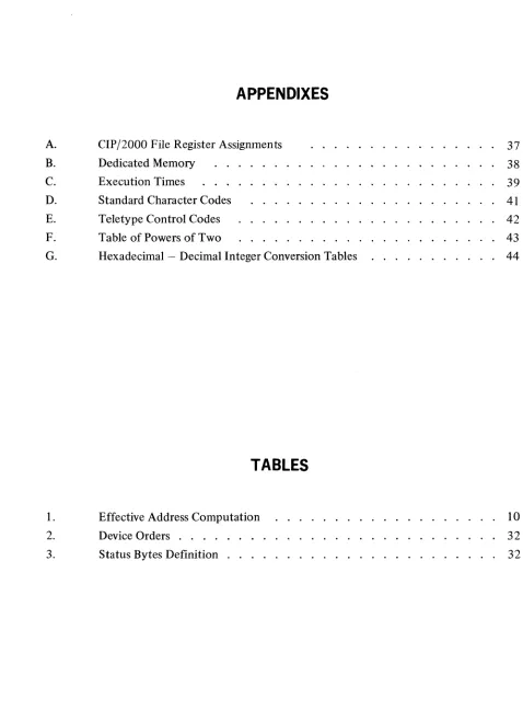
The eight-bit status byte input as the result of a status order has four bits which are common to all devices and four which are device dependent. This byte is input to the A or B register or to memory by an input instruction with device order 1. The meaning of the status bits is given in Table 4-2.
TABLE 3. STATUS BYTES DEFINITION
BIT
NUMBER
o
2
3
4-7
STATUS
Ready
Input Flag
Output Flag
Error
INSTRUCTION
DESCRIPTION
This bit is a 1-bit when the external device is in a ready state.
This bit is a 1-bit when the external device has a byte ready for input to the computer.
This bit is a 1-bit when the external device is ready to receive a byte from the computer.
This bit is a 1-bit when an error has occurred during a transfer. Errors may be timing, parity or device malfunction. This bit is cleared when the status byte is input.
Device Dependents
Three input and three output instructions provide for byte transfers with the A register, B register, and memory. When the transfer is to or from the A or B registers, only the eight low order bits are used.
IBA INPUT BYTE TO A
7 6 5
31
4
I
3 2 1.1,
f
I
5 4
I
3d
2 1 0
The order code, f, is sent to the device designated by d. An eight-bit data byte is input from the device and placed in the eight low order bits of A. The eight high order bits of A remain unchanged.
Affected: A
[image:36.612.116.545.205.458.2]I
I
(
I
(
[
I,
[
I
[
[
I
[
[
[
[
I
I
I
IBB INPUT BYTE TO B
32
7 6 5 4 I 3 2 1
The order code, f, is sent to the device designated by d. An eight-bit data byte is input from the device and placed in the eight low order bits of B. The eight high order bits of B remain unchanged.
Affected: B
IBM INPUT BYTE TO MEMORY
33
J
f
l,
~
, .H.
6 5
J
y Z
4 I 3 2 1 0
7 6 5 4 I 3 2 1 4 I 3 2 1
The order code, f, is sent to the device designated by d. An eight-bit byte is input from the device and stored in memory at the effective memory address.
Affected: Memory
OBA OUTPUT BYTE FROM A
7 6 5
39
4
I
3 2 1J
fl, : , .
The order code, f, is sent to the device designated by d. The contents of the eight low order bits of A are output to the device. The contents of A remain unchanged.
OBB OUTPUT BYTE FROM B
7 6 5
3A
4
I
3 2 1J
fl, : , ,
I
I
[
[
(
[
I
[
[
[
[
[
I
[
I
The order code, f, is sent to the device designated by d. The contents of the eight low order bits of B are output to the device. The contents of B remain unchanged.
OBM OUTPUT BYTE FROM MEMORY
7 6 •
38
• I
3 2 1J
dl, : .. H.
y
• I
3J
6 •z
• I 3 2 1 0
2 1
The order code, f, is sent to the device designated by d. The contents of the eight bit byte at the effective memory address is sent to the device. The contents of memory remain unchanged.
CONCURRENT INPUT/OUTPUT
The concurrent I/O allows for block transfers between the external device on the Byte I/O bus and memory at a maximum rate of 50,000 bytes per second. The transfers are fully automatic, and once started proceed without program intervention. Concurrent I/O takes priority over instruction execution and forces momentary sequence breaks during execution of long instructions such as multiply, divide and shifts to insure that concurrent I/O delays are not excessive.
ADDRESS CONTROL
Concurrent I/O addresses for each external device are controlled by a pair of two-byte address words. These two words are located in memory starting at an address equal to four times the device number. The first word is the current address (CA) and contains the address of the next memory byte to be used for the transfer. The second word is the End Address (EA) and contains the address of the last byte of the block. The first 128 locations in memory are reserved for storing concurrent I/O addresses for control of up to 32 external devices. The four bytes for each device have the following format:
4*ON
a
Current Address4*ON+2
,.
a
End Address,.
13 12 I 11 10 9 8 I 7 6•
4 I 3 2 1 0When the processor detects a request for concurrent I/O, it inputs an externally supplied address (ESA) from the requesting device. This byte must contain a device address in bits 6-1 and an output flag in bit 7. When bit 7 is a one, it signifies that the device is requesting an output transfer; otherwise an input is performed. The ESA is used by the processor to