FORCE COMPUTERS Inc./GmbH
All Rights Reserved
SYS68K/CPU-60
Technical Reference Manual
NOTE
The information in this document has been carefully checked and is believed to be entirely reliable. FORCECOMPUTERSmakes no warranty of any kind with regard to the material in this document, and assumes no responsibility for any errors which may appear in this document. FORCECOMPUTERSreserves the right
to make changes without notice to this, or any of its products, to improve reliability, performance, or design.
FORCECOMPUTERSassumes no responsibility for the use of any circuitry other than circuitry which is part of a product of FORCECOMPUTERSInc./GmbH. FORCECOMPUTERSdoes not convey to the purchaser of the product described herein any license under the patent rights of FORCECOMPUTERSInc./GmbH nor
World Wide Web: www.forcecomputers.com
24-hour access to on-line manuals, driver updates, and application notes is provided via SMART, our SolutionsPLUS customer support program
that provides current technical and services information.
Headquarters
The Americas
Europe
Asia
FORCECOMPUTERSInc. 5799 Fontanoso Way San Jose, CA 95138-1015
U.S.A.
Tel.: +1 (408) 369-6000 Fax: +1 (408) 371-3382 Email [email protected]
FORCECOMPUTERSGmbH Prof.-Messerschmitt-Str. 1 D-85579 Neubiberg/München
Germany
Tel.: +49 (89) 608 14-0 Fax: +49 (89) 609 77 93 Email [email protected]
FORCECOMPUTERSJapan KK Miyakeya Building 4F 1-9-12 Hamamatsucho Minato-ku, Tokyo 105
Japan
Contents
Table of Contents
Using This Manual . . . ix
1 Introduction . . . 1
1.1 Specification . . . 2
1.2 Ordering Information . . . 6
2 Installation . . . 7
2.1 Safety Note . . . 7
2.2 Installation Prerequisites and Requirements . . . 8
2.2.1 Requirements . . . 8
2.2.2 Terminal Connection . . . 9
2.2.3 Functional and Location Overview . . . 9
2.3 Automatic Power Up – Voltage Sensor and Watchdog Timer . . . 11
2.4 Switch Settings . . . 11
2.5 Front Panel . . . 15
2.6 SYS68K/CPU-60 Parameters and 16-bit Timers – CIO . . . 17
2.7 Serial I/O Ports – SCC. . . 17
2.8 SCSI. . . 21
2.9 Floppy Disk – FDC . . . 23
2.10 Ethernet – LAN . . . 23
2.11 VMEbus P2 Connector Pinout . . . 24
2.12 SYS68K/IOBP-1. . . 28
2.13 Testing the CPU Board Using VMEPROM . . . 30
3 Hardware . . . 33
3.1 SYS68K/CPU-60 Memory Map . . . 36
Contents
204077
J
une
1999
3.3 SYS68K/CPU-60 Parameters and Timers – CIO Z8536 . . . 40
3.3.1 MEM-60 DRAM Capacity and CIO1 Timer 3 . . . 41
3.3.2 Flash VPP, Floppy Disk Control, and CIO1 Timer 2 . . . 42
3.3.3 MODE x Rotary Switch Setting . . . 43
3.3.4 On-board DRAM Capacity and Automatic A24 Expansion . . . 44
3.3.5 Board ID and DIAG Display . . . 44
3.3.6 A24-to-A32 Address Translation . . . 45
3.4 68060 CPU . . . 45
3.4.1 Hardware Interface of the 68060 CPU . . . 45
3.4.2 Instruction Set of the 68060 CPU. . . 46
3.4.3 Vector Table of the 68060 CPU . . . 46
3.5 Watchdog Timer . . . 48
3.5.1 Watchdog Operation. . . 48
3.5.2 Watchdog Register Map . . . 49
3.6 RIALTO Bus Bridge . . . 50
3.6.1 Register Set. . . 50
3.6.2 Bridge Configuration Register . . . 50
3.7 FGA-002 Gate Array . . . 51
3.8 DRAM . . . 52
3.8.1 Register Set. . . 53
3.8.2 Memory Configuration Register . . . 54
3.8.3 Memory Diagnostic Register . . . 55
3.8.4 DRAM Performance. . . 56
3.8.5 Reading the DRAM Capacity. . . 57
3.8.6 DRAM Organization . . . 57
3.8.7 Cache Coherence and Snooping. . . 58
3.8.8 DRAM Access from the 68060 CPU . . . 59
3.8.9 DRAM Access via the VMEbus . . . 60
3.8.10 DRAM Access from the Ethernet-Controller. . . 61
3.8.11 DRAM Access from the SCSI-Controller . . . 61
3.9 User SRAM (factory option) . . . 61
Contents
3.10 System PROM . . . 62
3.10.1 Device Types for the System PROM . . . 63
3.10.2 Address Map of the System PROM . . . 63
3.10.3 Reading and Programming the System PROM . . . 64
3.11 Boot PROM . . . 64
3.11.1 Boot PROM Address Map and Factory Options . . . 66
3.11.2 Programming the Boot PROM . . . 67
3.12 User Flash . . . 68
3.12.1 Programming the User Flash . . . 68
3.13 Local SRAM . . . 69
3.13.1 Local SRAM Organization. . . 69
3.13.2 Devices Types for the Local SRAM . . . 70
3.13.3 Backup Power for the Local SRAM. . . 71
3.14 Real-Time Clock – RTC 72423 . . . 71
3.14.1 RTC Registers Address Map . . . 72
3.14.2 Reading from or Writing to the RTC 72423 . . . 73
3.14.3 Backup Power for the RTC 72423 . . . 74
3.15 VMEbus Interface . . . 75
3.15.1 Exception Signals SYSFAIL, SYSRESET, and ACFAIL . . . 76
3.15.2 Master Interface: Address Modifier (AM) Codes . . . 77
3.15.3 Master Interface: Data Transfer Size . . . 78
3.15.4 Master Interface: Burst to VMEbus . . . 80
3.15.5 Slave Interface: Access Address . . . 81
3.15.6 Slave Interface: DRAM Data Transfer Size. . . 81
3.15.7 Slave Interface: Address Modifier Decoding and A24 Slave Mode . . . 81
3.15.8 Slave Interface: Locked Cycles . . . 82
3.16 VMEbus Arbitration . . . 83
3.16.1 Single-Level VMEbus Arbiter . . . 83
3.16.2 VMEbus Requester. . . 83
3.16.3 VMEbus Release Modes . . . 84
3.16.4 VMEbus Grant Driver . . . 86
Contents
204077
J
une
1999
3.17.1 Slot-1 (System Controller) Functions. . . 87
3.17.2 Slot-1 Detection . . . 87
3.17.3 Slot-1 Status Register . . . 88
3.17.4 The SYSCLK Driver . . . 88
3.17.5 VMEbus Timer. . . 89
3.18 Serial I/O – SCC AM 85C30 . . . 89
3.18.1 RS-485 Configuration . . . 90
3.19 SCSI – 53C720SE. . . 92
3.19.1 SCSI Register Map . . . 93
3.19.2 Communication across the SCSI bus . . . 93
3.20 Floppy Disk – FDC 37C65C . . . 94
3.21 Ethernet – LAN AM 79C965A . . . 96
3.21.1 Register Access . . . 98
3.22 Reset Generation . . . 101
3.23 Information on Front Panel Devices . . . 103
4 Circuit Schematics . . . paginated separately 5 Data Sheets . . . paginated separately 5.1 CIO Z8536 5.2 FDC 37C65C 5.3 LAN AM 79C965A 5.4 RTC 72421 5.5 SCC AM 85C30 5.6 SCSI 53C720SE 6 VMEPROM . . . 125
6.1 Power-up Sequence . . . 126
6.2 Front Panel Related VMEPROM Features. . . 127
6.2.1 Reset Key . . . 127
6.2.2 Abort Key . . . 127
6.2.3 Rotary Switches . . . 128
Contents
6.3.1 Default Memory Usage of VMEPROM. . . 132
6.3.2 Default ROM Use of VMEPROM . . . 132
6.4 Devices and Interrupts Used by VMEPROM . . . 133
6.4.1 Addresses of the On-Board I/O Devices . . . 133
6.4.2 On-Board Interrupt Sources . . . 134
6.4.3 Off-Board Interrupt Sources. . . 134
6.4.4 The On-Board Real-Time Clock . . . 135
6.5 VMEPROM Commands . . . 135
6.5.1 ARB – Set the Arbiter of the CPU Board . . . 136
6.5.2 CONFIG – Search VMEbus for Hardware . . . 136
6.5.3 FERASE – Erase Flash Memories . . . 137
6.5.4 FGA – Change Boot Setup for Gate Array . . . 138
6.5.5 FLUSH – Set Buffered Write Mode. . . 139
6.5.6 FMB – FORCE Message Broadcast. . . 140
6.5.7 FPROG – Program Flash Memories . . . 141
6.5.8 FUNCTIONAL – Perform Functional Test . . . 142
6.5.9 INFO – Information about the CPU Board . . . 143
6.5.10 MEM – Set Data Bus Width of the VMEbus . . . 143
6.5.11 RUNINRAM – Run VMEPROM in RAM . . . 144
6.5.12 RUNINROM – Run VMEPROM in ROM . . . 145
6.5.13 SELFTEST – Perform On-Board Selftest . . . 145
6.6 Installing a New Hard Disk (UsingFRMTandINIT). . . 146
7 Appendix to VMEPROM . . . 151
7.1 Driver Installation . . . 151
7.1.1 VMEbus Memory. . . 151
7.1.2 SYS68K/SIO-1/2 . . . 152
7.1.3 SYS68K/ISIO-1/2 . . . 153
7.1.4 SYS68K/WFC-1 Disk Controller. . . 155
7.1.5 SYS68K/ISCSI-1 Disk Controller . . . 156
7.1.6 Local SCSI Controller . . . 157
Contents
204077
J
une
1999
7.4 Task Control Block Definitions . . . 162
7.5 Interrupt Vector Table of VMEPROM . . . 165
7.6 Benchmark Source Code. . . 168
7.7 Modifying Special Locations in ROM . . . 174
7.8 Binding Applications to VMEPROM . . . 177
7.8.1 Using External Memory . . . 177
7.8.2 Using System Flash Memory . . . 177
8 FGA Boot . . . 179
8.1 Boot Sequence . . . 179
8.2 Debugger Commands . . . 182
8.2.1 AS – Line Assembler . . . 182
8.2.2 BANNER – Display Banner Again . . . 184
8.2.3 CONT – Continue with Calling Routine . . . 184
8.2.4 DI – Disassembler . . . 184
8.2.5 DRAMINIT – Initialize DRAM. . . 185
8.2.6 FERASE – Erase Flash Memories . . . 185
8.2.7 FPROG – Program Flash Memories . . . 186
8.2.8 GO – Go to Subroutine. . . 188
8.2.9 LO – Load S-Records to Memory . . . 188
8.2.10 NETLOAD – Load File via Network to Memory . . . 190
8.2.11 NETSAVE – Save Data via Network to File . . . 191
8.2.12 SETUP – Change Initialization Values . . . 193
8.2.13 SLOT – Change Slot Number and VMEbus Slave Address . . . 194
8.2.14 VMEADDR – Change VMEbus Slave Address . . . 195
8.3 FGA Boot Utility Functions . . . 196
8.3.1 Extended Flash Memory Programming . . . 197
8.3.2 Erase Flash Memories . . . 198
8.3.3 Get System Values in SRAM . . . 199
8.3.4 Get Application Values in SRAM . . . 200
8.3.5 Get Ethernet Number . . . 200
Tables and Figures
List of Tables and Figures
Page Tab./Fig.
Tables and Figures
2040
77
J
une
1999
Page Tab./Fig.
Using This Manual
Using This Manual
This section does not provide information on the product but on common features of the manual itself:
• its structure,
• special layout conventions,
• and related documents.
Audience of the Manual
This Technical Reference Manual is intended for hard- and software de-velopers installing and integrating the SYS68K/CPU-60 into their sys-tems.
Overview of the Manual
This Technical Reference Manual provides a comprehensive hardware and software guide to your board.
i
IMPORTANT Please take a moment to examine the “Table of Contents” to see how this documentation is structured. This will be of value to you when looking for information in the future.
It includes
• a brief overview of the product, the specifications, the ordering infor-mation: see section 1 “Introduction” on page 1.
• the installation instructions for powering up the board: see section 2 “Installation” on page 7. It includes the default configuration (switches and the like), initialization, and connector pinouts.
The installation instructions also appear as the product’s installation guide – a separate manual delivered together with each product shipped.
• a detailed hardware description: see section 3 “Hardware” on page 33.
• the circuit schematics of the board for reference purposes.
The circuit schematics are packaged separately to enable easy updat-ing. They will always be shipped together with this manual. Therefore:
Using This Manual
204
077
J
une
1999
• the data sheets of board components that are relevant for configuring and integrating the board in systems. The following data sheets are delivered:
– Motorola 68060 (delivered as a separate manual)
– CIO Z8536
– FDC 37C65C: pin-to-pin compatible with industry standard WD37C65C
– LAN AM 79C965A
– RTC 72421
– SCC AM 85C30
– SCSI 53C720SE
The data sheets are packaged separately to enable easy updating. They are always shipped together with this manual. Therefore:
☞ Insert the data sheets now: see section 5 “Data Sheets”. • a detailed description of VMEPROM and FGA Boot which control the
CPU board operations: see section 6 “VMEPROM” on page 125, section 7 “Appendix to VMEPROM” on page 151, and section 8 “FGA Boot” on page 179.
There is additional space allocated in the manual for user notes, modifi-cations, etc.
Referenced Manuals
Table 1 Referenced manuals separately available from FORCE COMPUTERS Referenced manual Pages referring to the manual IOPI-2 User’s Installation 24
Using This Manual
Publication History of the Manual
Fonts, Notations and Conventions Table 2 History of manual publication
Edition Date Description
1 July 1996 First print
2 August 1996 Editorial Changes
2.1 July 1997 Extended NETLOAD and NETSAVE FGA Boot debugger commands. Corrected FDC register map, correct-ed pinout of front-panel serial I/O port, and corrected units for VME-BUSTIMERbits (memory configura-tion register).
2.2 January 1999 Switch settings for RS-485 correct-ed, RS-485 configuration described
Table 3 Fonts, Notations and Conventions Notation Description
0000.000016 Typical notation for hexadecimal numbers (digits are
0 through F), e.g. used for addresses and offsets. Note the dot marking the 4th (to its right) and 5th (to its left) digit.
00008 Same for octal numbers (digits are 0 through 7) 00002 Same for binary numbers (digits are 0 and 1)
Program Typical character format used for names, values, and the like that should be used typing literally the same word. Also used for on-screen-output.
Using This Manual
204
077
J
une
1999
Icons for Ease of Use: Safety Notes and Tips & Tricks
There are 3 levels of safety notes used in this manual which are described below in brief by displaying a typical layout example.
Be sure to always read and follow the safety notes of a section first – before acting as documented in the other parts of the section.
CAUTION Dangerous situation: injuries of people and severe damage to objects pos-sible.
!
NOTICE Possibly dangerous situation: no injuries to people but damage to objects possible.
i
Introduction
1
Introduction
The SYS68K/CPU-60 is a high performance single-board computer pro-viding an A32/D32 VMEbus interface including DMA. It is based on
• the 68060 CPU,
• the FORCE gate array FGA-002,
• and the VMEbus.
Memory The SYS68K/CPU-60 provides up to 32 Mbyte DRAM on-board (field upgradable). Up to 128 Mbyte DRAM are available with the SYS68K/MEM-60 extension module. Up to 2 Mbyte user SRAM, up to 512 Kbyte local SRAM with battery backup, up to 8 Mbyte system PROM, and up to 1 Mbyte boot PROM are available.
The shared DRAM is accessible from the 68060 CPU, the FGA-002 chip DMA controller, the SCSI chip DMA controller, the LAN on-chip DMA controller, and also from VMEbus masters.
Interfaces The SYS68K/CPU-60 incorporates SCSI-2, Ethernet, and serial I/O on-board to provide full single-on-board computer functionality.
The SYS68K/CPU-60 has 2 serial ports at the front panel permitting a console port for download and data communication. Both ports use stan-dard 9-pin D-Sub connectors.
CPU speed The 68060 CPU runs at 50 MHz and has cache snooping support for al-ternate master access to the shared DRAM.
Specification Introduction
2040
77
J
une
1999
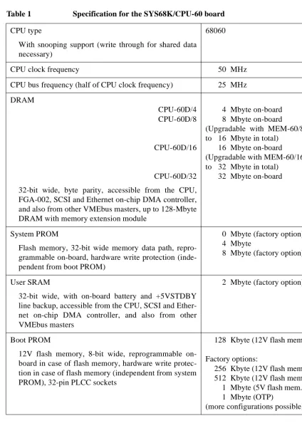
[image:16.612.104.529.97.692.2]1.1
Specification
Table 1 Specification for the SYS68K/CPU-60 board CPU type
With snooping support (write through for shared data necessary)
68060
CPU clock frequency 50 MHz
CPU bus frequency (half of CPU clock frequency) 25 MHz
DRAM
CPU-60D/4 CPU-60D/8
CPU-60D/16
CPU-60D/32
32-bit wide, byte parity, accessible from the CPU, FGA-002, SCSI and Ethernet on-chip DMA controller, and also from other VMEbus masters, up to 128-Mbyte DRAM with memory extension module
4 Mbyte on-board 8 Mbyte on-board (Upgradable with MEM-60/8 to 16 Mbyte in total)
16 Mbyte on-board (Upgradable with MEM-60/16 to 32 Mbyte in total)
32 Mbyte on-board
System PROM
Flash memory, 32-bit wide memory data path, repro-grammable on-board, hardware write protection (inde-pendent from boot PROM)
0 Mbyte (factory option) 4 Mbyte
8 Mbyte (factory option)
User SRAM
32-bit wide, with on-board battery and +5VSTDBY line backup, accessible from the CPU, SCSI and Ether-net on-chip DMA controller, and also from other VMEbus masters
2 Mbyte (factory option)
Boot PROM
12V flash memory, 8-bit wide, reprogrammable on-board in case of flash memory, hardware write protec-tion in case of flash memory (independent from system PROM), 32-pin PLCC sockets
128 Kbyte (12V flash mem.)
Factory options:
256 Kbyte (12V flash mem.) 512 Kbyte (12V flash mem.) 1 Mbyte (5V flash mem.) 1 Mbyte (OTP)
Introduction Specification
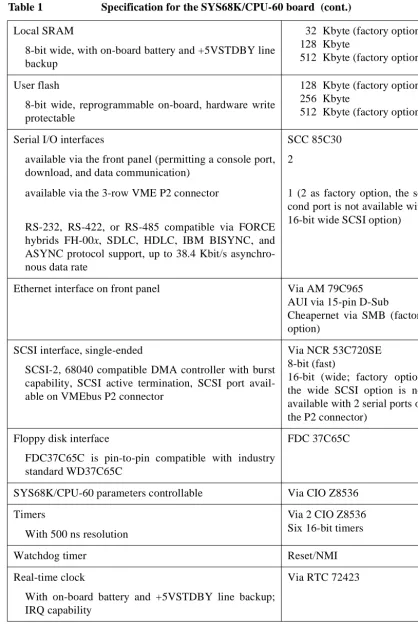
Local SRAM
8-bit wide, with on-board battery and +5VSTDBY line backup
32 Kbyte (factory option) 128 Kbyte
512 Kbyte (factory option)
User flash
8-bit wide, reprogrammable on-board, hardware write protectable
128 Kbyte (factory option) 256 Kbyte
512 Kbyte (factory option)
Serial I/O interfaces
available via the front panel (permitting a console port, download, and data communication)
available via the 3-row VME P2 connector
RS-232, RS-422, or RS-485 compatible via FORCE hybrids FH-00x, SDLC, HDLC, IBM BISYNC, and ASYNC protocol support, up to 38.4 Kbit/s asynchro-nous data rate
SCC 85C30
2
1 (2 as factory option, the se-cond port is not available with 16-bit wide SCSI option)
Ethernet interface on front panel Via AM 79C965 AUI via 15-pin D-Sub
Cheapernet via SMB (factory option)
SCSI interface, single-ended
SCSI-2, 68040 compatible DMA controller with burst capability, SCSI active termination, SCSI port avail-able on VMEbus P2 connector
Via NCR 53C720SE 8-bit (fast)
16-bit (wide; factory option, the wide SCSI option is not available with 2 serial ports on the P2 connector)
Floppy disk interface
FDC37C65C is pin-to-pin compatible with industry standard WD37C65C
FDC 37C65C
SYS68K/CPU-60 parameters controllable Via CIO Z8536
Timers
With 500 ns resolution
Via 2 CIO Z8536 Six 16-bit timers
Watchdog timer Reset/NMI
Real-time clock
With on-board battery and +5VSTDBY line backup; IRQ capability
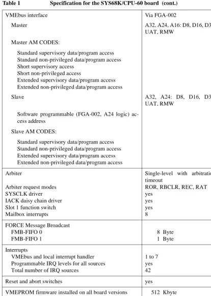
[image:17.612.105.524.62.688.2]Specification Introduction
2040
77
J
une
1999
VMEbus interface
Master
Master AM CODES:
Standard supervisory data/program access Standard non-privileged data/program access Short supervisory access
Short non-privileged access
Extended supervisory data/program access Extended non-privileged data/program access
Slave
Software programmable (FGA-002, A24 logic) ac-cess address
Slave AM CODES:
Standard supervisory data/program access Standard non-privileged data/program access Extended supervisory data/program access Extended non-privileged data/program access
Via FGA-002
A32, A24, A16: D8, D16, D32, UAT, RMW
A32, A24: D8, D16, D32, UAT, RMW
Arbiter
Arbiter request modes SYSCLK driver
IACK daisy chain driver Slot 1 function switch Mailbox interrupts
Single-level with arbitration timeout
ROR, RBCLR, REC, RAT yes
yes yes 8
FORCE Message Broadcast FMB-FIFO 0
FMB-FIFO 1
8 Byte 1 Byte
Interrupts
VMEbus and local interrupt handler Programmable IRQ levels for all sources Total number of IRQ sources
1 to 7 yes 42
Reset and abort switches yes
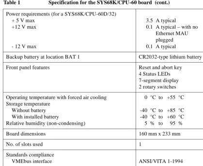
[image:18.612.108.523.63.644.2]Introduction Specification
Power requirements (for a SYS68K/CPU-60D/32) + 5 V max
+12 V max
- 12 V max
3.5 A typical
0.1 A typical – with no Ethernet MAU plugged 0.1 A typical
Backup battery at location BAT 1 CR2032-type lithium battery
Front panel features Reset and abort key
4 Status LEDs 7-segment display 2 rotary switches
Operating temperature with forced air cooling Storage temperature
Without battery With installed battery
Relative humidity (non-condensing)
0 °C to +55 °C
-40 °C to +85 °C -40 °C to +60 °C 5 % to 95 %
Board dimensions 160 mm x 233 mm
No. of slots used 1
Standards compliance
[image:19.612.106.526.64.406.2]VMEbus interface ANSI/VITA 1-1994
Ordering Information Introduction
2040
77
J
une
1999
1.2
Ordering Information
Table 2 Ordering information for the SYS68K/CPU-60
Product name Product description
SYS68K/CPU-60D/4, …/8, …/16, …/32
MEM-60/8, …/16
50 MHz 68060 based CPU board (“60D” in product name, with “60E” it is based on a 66 MHz 68060), 32-bit DMA, 4 (8/16/32) Mbyte shared memory, 2 serial I/O channels (RS-232), SCSI, floppy disk and Ethernet inter-face, VMEPROM documentation not included.
SYS68K/CPU-60D/8 field upgradable to a total of 16 Mbyte shared memory by installing the MEM-60/8 mem-ory module (SYS68K/CPU-60x/16 field upgradable to a total of 32 Mbyte by MEM-60/16).
SYS68K/CPU-60Lite/4 50 MHz 68LC060 based CPU board, 32-bit DMA, 4
(8/16/32) Mbyte shared memory, 2 serial I/O channels (RS-232), VMEPROM documentation not included.
UM SYS68K/CPU-60 SYS68K/CPU-60 Technical Reference Manual Set
in-cluding VMEPROM and FGA-002 manuals.
UM SYS68K/FGA-002 FORCE Gate Array (FGA-002) User's Manual
UM SYS68K/VMEPROM/32 VMEPROM User's Manual for 32-bit CPUs
SYS68K/IOBP-1 Rear I/O paddel panel for single board computers
provid-ing connectors for 8-bit SCSI, floppy disk drive and one serial I/O port.
IOPI-2 Rear I/O paddel panel for single board computers
provid-ing connectors for 8-bit SCSI, floppy disk drive and one serial I/O port.
SYS68K/CABLE 9-25 SET Set of 4 adapter cables 9-pin D-Sub male connector to
25-pin D-Sub female connector, length 2 m (SYS68K/CPU-60)
Hybrids for the serial I/O interfaces (10 hybrids per set):
SYS68K/FH002/SET RS-232 protocol
SYS68K/FH003/SET RS-422 protocol
Installation Safety Note
2
Installation
2.1
Safety Note
To ensure proper functioning of the product during its usual lifetime, take the following precautions before handling the board.
CAUTION Malfunction or damage to the board or connected components
Electrostatic discharge and incorrect board installation and uninstallation can damage circuits or shorten their lifetime.
• Before installing or uninstalling the board, read this Installation sec-tion.
• Before installing or uninstalling MEM-60 memory modules, read the
MEM-60 Installation Guide packaged together with the modules.
• Before installing or uninstalling the board, in a VME rack turn off the power.
• Before touching integrated circuits, ensure that you are working in an electrostatic free environment.
• Ensure that the board is connected to the VMEbus via both the P1 and the P2 connectors and that power is available on both of them.
• When operating the board in areas of strong electromagnetic radiation, ensure that the board
– is bolted on the VME rack
– and shielded by closed housing.
CAUTION Damage of components caused by inappropriate floppy drive installation There are floppy disk drives that provide means to connect the floppy disk drive frame electrically with DC ground, e.g., by inserting a jumper on the floppy disk drive.
• Before installing a floppy disk drive, always make sure that the floppy disk drive’s frame is not electrically connected with DC ground.
!
NOTICE Damaging SYS68K/CPU-60 components
Installation Prerequisites and Requirements Installation
2040
77
2
–
3
J
une
1999
CAUTION Maintenance of the CPU board:
The board is designed to be maintenance-free. However, note that a Lith-ium battery is installed on the board. The battery provides a data retention of 7 years summing up all periods of actual battery use. Therefore, FORCE COMPUTERS assumes that there usually is no need to exchange the Lithium battery except for example in the case of long-term spare part handling. Observe the following safety notes:
• Incorrect exchange of Lithium batteries can result in a hazardous explosion.
• Exchange the battery before 7 years of actual battery use have elapsed.
• Exchanging the battery always results in data loss of the devices which use the battery as power backup. Therefore, back up affected data before exchanging the battery.
• Always use the same type of Lithium battery as is already installed.
• When installing the new battery ensure that the marked dot on top of the battery covers the dot marked on the chip.
• Used batteries have to be disposed according to your country’s legisla-tion.
2.2
Installation Prerequisites and Requirements
i
IMPORTANT Before powering up
• check this section for installation prerequisites and requirements
• and check the consistency of the current switch settings (see section 2.4 “Switch Settings” on page 11).
2.2.1 Requirements
The installation requires only
• a power supply
• and a VMEbus backplane with P1 and P2 connector.
Power supply The power supply must meet the following specifications:
• required for the processor board: +5 V (3.5 A typical for a SYS68K/CPU-60D/32, 3.0 A typical for a SYS68K/CPU-60D/4)
• required for the RS-232 serial interface and the Ethernet interface:
– +12 V (0.1 A typical – with no Ethernet MAU plugged)
Installation Installation Prerequisites and Requirements
2.2.2 Terminal Connection
For the initial power-up, a terminal can be connected to the standard 9-pin D-Sub connector of serial port 1, which is located at the front panel (see section 2.7 “Serial I/O Ports – SCC” on page 17).
2.2.3 Functional and Location Overview
[image:23.612.109.523.215.568.2]Figure 1 gives a functional overview, figure 2 highlights the locations of the important SYS68K/CPU-60 components.
Figure 1 Block diagram of the SYS68K/CPU-60
FDC RTC Boot PROM User flash (local flash) SCC CIO CPU bus (060 bus) VESA local bus (VL bus)
FLXI bus (020 bus) Memory bus I/O bus 4 LEDs Hex. Displ. 2 rotary sw. Reset key
Installation Prerequisites and Requirements Installation 2040 77 2 – 3 J une 1999
Figure 2 Location diagram of the SYS68K/CPU-60 (schematic)
ID-ROM Bottom 4 LEDs SERIAL A B O R T ETHERNET 68060 CPU Ethernet SCSI Backup battery FDC SCC NVRAM RTC Boot PROM # 1 J 70 # 2 J 71 User flash J31 MEM-60 connector SW12 SW11 SW9 SW7 SW5 SW10
P2 connector P1 connector
2 rotary switches Top BM SYSF MODE DIAG Status display 1 2 Front panel RUN UL
1 2 RE
S E T CIO 2 CIO 1 RIALTO bus bridge Memory control
Watchdog timer System PROM DRAM Bank 2
(8 of 9)
FGA-002
DRAM Bank 1 (9 of 9) DRAM Bank 2 (1 of 9)
User SRAM SW6 10Base2
AUI (option)
Ser. I/O 1 J21
Installation Automatic Power Up – Voltage Sensor and Watchdog
2.3
Automatic Power Up – Voltage Sensor and Watchdog Timer
In the following situations the CPU board will automatically be reset and proceed with a normal power up:
Voltage sensor • The voltage sensor generates a reset when the voltage level drops below 4.75 V.
Watchdog timer • Per factory default the watchdog timer is disabled. If the watchdog timer is enabled, it generates a non-maskable interrupt (NMI) followed by a pseudo power up when it is not re-triggered. The watchdog timer can be enabled by software.
2.4
Switch Settings
The following table lists the function and the default settings of all switches shown in figure 2 “Location diagram of the SYS68K/CPU-60 (schematic)” on page 10.
i
IMPORTANT • Before powering up the board check the current switch settings for consistency.
[image:25.612.180.521.429.666.2]• SW6-1, SW6-2, SW6-3, and SW6-4 will only be read on a power up.
Table 3 Switch settings
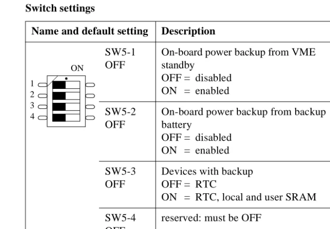
Name and default setting Description SW5-1
OFF
On-board power backup from VME standby
OFF = disabled ON = enabled
SW5-2 OFF
On-board power backup from backup battery
OFF = disabled ON = enabled
SW5-3 OFF
Devices with backup OFF = RTC
ON = RTC, local and user SRAM
SW5-4 OFF
reserved: must be OFF ON
Switch Settings Installation
2040
77
2
–
3
J
une
1999
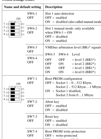
SW6-1 OFF
Slot 1 auto-detection OFF = enabled
ON = disabled (also called manual mode)
SW6-2 OFF
Slot 1 manual mode: only available when SW6-1 = ON
OFF = disabled ON = enabled
SW6-3 OFF
VMEbus arbitration level (BRx* signals)
SW6-3 SW6-4 Level
OFF OFF = level 3 (BR3*) OFF ON = level 2 (BR2*) ON OFF = level 1 (BR1*) ON ON = level 0 (BR0*) SW6-4
OFF
SW7-1 OFF
Boot PROM configuration OFF = Socket 1 – 0…512 Kbyte,
Socket 2 – 512 Kbyte…1 Mbyte ON = Socket 1 disabled,
Socket 2 from 0…1 Mbyte
SW7-2 OFF
Abort key OFF = enabled ON = disabled
SW7-3 OFF
Reset key OFF = enabled ON = disabled
SW7-4 OFF
[image:26.612.200.529.70.523.2]Boot PROM write protection OFF = write-protected ON = writing enabled Table 3 Switch settings (cont.)
Name and default setting Description
ON
1 2 3 4
ON
Installation Switch Settings
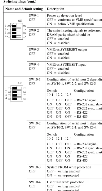
SW9-1 OFF
Power up detection level
OFF = conforms to VME specification ON = below VME specification
SW9-2 OFF
The switch setting signals to software: DRAM parity check should be
OFF = enabled ON = disabled
SW9-3 OFF
VMEbus SYSRESET output OFF = enabled
ON = disabled
SW9-4 OFF
VMEbus SYSRESET input OFF = enabled
ON = disabled
SW10-1 OFF
Configuration of serial port 2 depending on SW10-1, SW12-2, and SW12-3
Switch Configuration 10-1 12-2 12-3
OFF OFF OFF = RS-232 async. ON ON OFF = RS-232 sync. slave OFF OFF ON = RS-232 sync. master ON ON ON = RS-422
ON ON OFF = RS-485
SW10-2 OFF
Configuration of serial port 1 depending on SW10-2, SW12-1, and SW12-4
Switch Configuration 10-2 12-1 12-4
OFF OFF OFF = RS-232 async. ON OFF ON = RS-232 sync. slave OFF ON OFF = RS-232 sync. master ON ON ON = RS-422
ON OFF ON = RS-485
SW10-3 OFF
System PROM write protection OFF = writing enabled
ON = write-protected
SW10-4 OFF
[image:27.612.195.525.64.682.2]User flash write protection OFF = writing enabled ON = write-protected Table 3 Switch settings (cont.)
Name and default setting Description
ON
1 2 3 4
ON
Switch Settings Installation
2040
77
2
–
3
J
une
1999
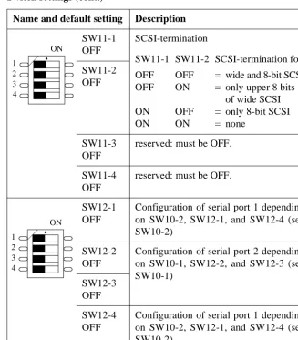
SW11-1 OFF
SCSI-termination
SW11-1 SW11-2 SCSI-termination for
OFF OFF = wide and 8-bit SCSI OFF ON = only upper 8 bits
of wide SCSI ON OFF = only 8-bit SCSI
ON ON = none
SW11-2 OFF
SW11-3 OFF
reserved: must be OFF.
SW11-4 OFF
reserved: must be OFF.
SW12-1 OFF
Configuration of serial port 1 depending on SW10-2, SW12-1, and SW12-4 (see SW10-2)
SW12-2 OFF
Configuration of serial port 2 depending on SW10-1, SW12-2, and SW12-3 (see SW10-1)
SW12-3 OFF
SW12-4 OFF
[image:28.612.199.526.72.445.2]Configuration of serial port 1 depending on SW10-2, SW12-1, and SW12-4 (see SW10-2)
Table 3 Switch settings (cont.)
Name and default setting Description
ON
1 2 3 4
ON
Installation Front Panel
2.5
Front Panel
The features of the front panel are described in the following table. For a location diagram see figure 2 “Location diagram of the SYS68K/CPU-60 (schematic)” on page 10.
i
IMPORTANT Toggling the reset key and the abort key at the same time has a special function which is described in the boot software description of the
FORCE Gate Array FGA-002 User's Manual.
Table 4 Front panel features
Device Description
RESET Mechanical reset key: When enabled and toggled it instantaneously affects the CPU board by generating a reset. Depending on SW9-3 the reset generates a VMEbus SYSRESET (see “SW9-3” on page 13). A reset of all on-board I/O devices and the CPU is performed when the reset key is pushed to the UP po-sition. RESET is held active until the key is back in the DOWN position but at least 200 ms guaranteed by a local timer. Power fail (below approximately 4.7 Volts) and power up – both lasting at minimum 200 ms to 300 ms – also force a reset to start the CPU board.
For information on enabling the key, see “SW7-3” on page 12.
ABORT Mechanical abort key: When enabled and toggled it instantaneously affects the CPU board by generating an interrupt request (IRQ) on level 7 via the FGA-002. The abort key is activated in UP position and deactivated in DOWN position.
This allows to implement an abort of the current pro-gram, to trigger a self-test or to start a maintenance program.
For information on enabling the key, see “SW7-2” on page 12.
Front Panel Installation
2040
77
2
–
3
J
une
1999
MODE 1 MODE 2
2 hexadecimal rotary switches, each decoded with 4 bit. The status of the rotary switch can be read in the CIO1 port A data register (including MODE x status register). Default for both rotary switches: F16
RUN 68060 CPU status: green
normal operation
red
the processor is halted or reset is active
BM VME busmaster LED: green
if the CPU board accesses the VMEbus as VMEbus master
off
otherwise
SYSF SYSFAIL LED:
red
if SYSFAIL is asserted from the FGA-002
off
otherwise
UL User LED: Software programmable by the RIALTO Bridge configuration register (BCR). Possible status: green or off.
SERIAL 1 2 standard 9-pin D-Sub connectors for serial interface (see section 2.7 “Serial I/O Ports – SCC” on page 17) SERIAL 2
ETHERNET (AUI or 10base2)
[image:30.612.200.526.68.615.2]15-pin AUI Ethernet connector for thick-wire Ethernet (802.3/10base5, see section 2.10 “Ethernet – LAN” on page 23); as factory option Cheapernet (802.3/10base2) is available via an SMB connector instead of the Ethernet AUI interface. An adapter from SMB type to BNC type connector is available from FORCE COMPUTERS.
Table 4 Front panel features (cont.)
Installation SYS68K/CPU-60 Parameters and 16-bit Timers – CIO
2.6
SYS68K/CPU-60 Parameters and 16-bit Timers – CIO
Configurable parameters
Via the two CIO Z8536 devices several parameters can be configured or read, respectively: front panel rotary switch setting, front panel status dis-play, on-board and MEM-60 DRAM size code, CPU-board code, avail-ability of VME A24 extension, AUX DMA direction, programming voltage VPP, configuration of FDC 37C65C control signals, ID-ROM (serial EEPROM), and the six 16-bit timers.
Timers Six 16-bit timers with a resolution of 500 ns are available.
2.7
Serial I/O Ports – SCC
Devices: 2 CIO Z8536
Frequency 4 MHz
Package 44-pin PLCC
Accessible from 68060 CPU
Access address
for device #1 FF80.0C0016
for device #2 FF80.0E0016
Port width Byte
Interrupt request level Software programmable
FGA-002 interrupt Local IRQ #4
Device: SCC AM 85C30
Frequency 8 MHz, 14.7456 MHz
Package 44-pin PLCC
Accessible from 68060 CPU
Access address FF80.200016
Port width Byte
Interrupt request level Software programmable
Serial I/O Ports – SCC Installation
2040
77
2
–
3
J
une
1999
The two serial I/O ports are available via 9-pin standard D-Sub connec-tors at the front panel. The SERIAL 1 front-panel port is also available on the VMEbus P2 connector (see section 2.11 “VMEbus P2 Connector Pi-nout” on page 24). All ports may be configured for RS-232, RS-422, and RS-485 standard conformance via installing the respective FORCE COMPUTERS hybrids FH-00x.
Factory option As factory option the SERIAL 2 front-panel port is also available on the VMEbus P2 connector (see section 2.11 “VMEbus P2 Connector Pinout” on page 24). The SERIAL-2-on-P2 and the wide-SCSI factory option are not available simultaneously.
Jumpers and terminations
There are no on-board jumpers to configure the serial ports and no line terminations for RS-422 and RS-485 interfaces. If termination resistors are required to compensate various cable lengths and to reduce signal re-flections, they must be installed externally to the SYS68K/CPU-60 (e.g. via a cable connector). The resistor value is application dependent, but a recommended value is 1000Ω.
Connector availability
Both serial I/O ports 1 and 2 are available via a front-panel 9-pin D-Sub connector, per factory default only serial I/O port 1 is available via the P2 connector:
• serial I/O port 1 is wired to the front-panel connector labeled SERIAL 1 and to the VMEbus P2 connector with 7 lines,
• serial I/O port 2 is wired to the front-panel connector labeled SERIAL 2. As a factory option, serial I/O port 2 may also be wired to the VMEbus P2 connector (not available together with wide-SCSI fac-tory option).
For the connection to the IOBP-1 back panel, see section 2.12 “SYS68K/IOBP-1” on page 28.
Installation Serial I/O Ports – SCC
Table 5 Pinout of the front panel serial I/O ports config. for RS-232
Pin Signal
1 DCD (Data Carrier Detect, input)
2 RXD (Receive Data, input and out-put)
3 TXD (Transmit Data, output)
4 DTR (Data Terminal Ready, output)
5 GND (Ground)
6 DSR (Data Set Ready, input and out-put)
7 RTS (Request to Send, output)
8 CTS (Clear to Send, input)
9 GND (Ground, output): supplied by FH-002 hybrid
1
5
6
[image:33.612.200.525.71.329.2]9
Table 6 Pinout of the front panel serial I/O ports config. for RS-422
Pin Signal
1 TXD– (Transmit Data, output)
2 RTS– (Request to Send, output)
3 CTS+ (Clear to Send, input)
4 RXD+ (Receive Data, input)
5 GND (Signal GND)
6 TXD+ (Transmit Data, output)
7 RTS+ (Request to Send, output)
8 CTS– (Clear to Send, input)
9 RXD– (Receive Data, input)
1
5
6
Serial I/O Ports – SCC Installation
2040
77
2
–
3
J
une
1999
i
IMPORTANT In case of the RS-485 configuration connect the pins 3 and 7 to GND via the RS-485 cable, e.g. by connecting them to the pins 2 and 8, respectively.
Default port setup
• FH-002 installed for RS-232 support
• Asynchronous communication
• 9600 Baud, 8 data bits, 1 stop bit, no parity
• Hardware handshake protocol
Interface options To easily vary the serial I/O interfaces according to the application’s needs FORCE COMPUTERS has developed RS-232, RS-422, and RS-485 hybrid modules: the FH-002, FH-003/FH-422T, and FH-007. The difference between FH-003 and FH-422T is that FH-422T has inter-nal termination resistors. For each serial I/O port one of these 21-pin sin-gle in-line (SIL) hybrids is installed on-board:
• serial I/O port 1: hybrid installed in location J21
[image:34.612.199.526.73.318.2]• serial I/O port 2: hybrid installed in location J22
Table 7 Pinout of the front panel serial I/O ports config. for RS-485
Pin Signal
1 RX-,
TX-2 GND
3 To be connected to GND via RS-485 cable
4 n.c.
5 GND
6 RX+, TX+
7 To be connected to GND via RS-485 cable
8 GND
9 n.c.
1
5
6
Installation SCSI
After installing the correct hybrid for the port under consideration the port has to be configured accordingly by using the appropriate switch set-ting. Thereby, the following options are selectable:
• FH-002 installed:
– RS-232 asynchronous
– RS-232 synchronous master
– RS-232 synchronous slave
• FH-003/FH-422T installed:
– RS-422
• FH-007 installed:
– RS-485
Switches selecting serial I/O options
The following switches apply to the port configuration:
• port 1: SW10-2, SW12-1, SW12-4 (see “SW10-2” on page 13),
• port 2: SW10-1, SW12-2, SW12-3 (see “SW10-1” on page 13).
2.8
SCSI
The SCSI 53C720SE provides an 8-bit SCSI interface which is routed to the VMEbus P2 connector. The 8-bit SCSI interface at the VMEbus P2 is pinout compatible to the CPU-30 and CPU-40 (with EAGLE-01 or EA-GLE-10/11).
The local bus interface is 32-bit wide and able to transfer data via the DMA controller of the SCSI 53C720SE.
Device: SCSI 53C720SE
Frequency CPU bus frequency
Package PQ160
Accessible from 68060 CPU
Access address FFF8.000016
Port width Long
Interrupt request level Software programmable
SCSI Installation
2040
77
2
–
3
J
une
1999
The active termination can be selected by means of switches (see “SW11-2” and “SW11-1” on page 14).TERMPWRis supported.
Factory option A 16-bit single-ended SCSI interface (wide SCSI) which is routed to the VMEbus P2 connector is available as factory option (see section 2.11 “VMEbus P2 Connector Pinout” on page 24). The wide-SCSI and the SERIAL-2-on-P2 factory option are not available simultaneously.
SCSI Bus Termination
i
IMPORTANT According to the SCSI specification, the interconnecting flat cable must be terminated at both ends.
• Before connecting SCSI devices ensure correct SCSI bus termination:
– If the CPU board is not located at either end of the cable, the termi-nation must be disabled.
– If the CPU board is located at the cable’s end, the termination must be enabled.
On the SYS68K/CPU-60 the termination of the SCSI bus is done by ac-tive terminators with a disconnect feature. This allows the outputs to be shut down to remove the terminator from the SCSI bus. It also reduces the standby power.
The disconnect input of the terminators is controlled by SW11-1 and SW11-2: default “OFF OFF = wide and 8-bit SCSI”, see page 14.
SCSI bus
terminator power
The power for the terminator of any SCSI device will be provided from the CPU board directly, or from the SCSI bus itself. If the termination power is not delivered from any other SCSI device, it is delivered from the CPU board.
The TERMPWR (terminator power) supply from the CPU board is pro-tected by a self-resetting fuse (1A max.) and a diode in series, as defined in the SCSI specification.
Installation Floppy Disk – FDC
2.9
Floppy Disk – FDC
The FDC signals are available at the VMEbus P2 connector (see section 2.11 “VMEbus P2 Connector Pinout” on page 24).
An I/O back panel can be plugged onto the rear side of the backplane to interface to standard FDC connectors (see section 2.12 “SYS68K/IOBP-1” on page 28).
2.10 Ethernet – LAN
The Ethernet AUI interface is available at the front panel via a 15-pin D-Sub connector. As factory option Cheapernet is available via an SMB connector instead of the Ethernet AUI interface.
Device: FDC 37C65C
Frequency 16 MHz
Package 44-pin PLCC
Accessible from 68060 CPU
Access address FF80.380016
Port width Byte
Interrupt request level Software programmable
FGA-002 interrupt Local IRQ #1
Device: LAN AM 79C965A
Frequency 68060 CPU bus frequency
Package PQ160
Accessible from 68060 CPU
Access address FFF0.000016
Port width Word only in 16-bit mode, long in 32-bit mode
Interrupt request level Software programmable
VMEbus P2 Connector Pinout Installation
2040
77
2
–
3
J
une
1999
The CPU bus interface is 32-bit wide and able to transfer data via the DMA controller of the AM 79C965A.
The following table shows the pinout of the factory default Ethernet con-nector:
Ethernet address The CPU board’s Ethernet address is displayed in the banner when enter-ing FGA Boot.
2.11 VMEbus P2 Connector Pinout
I/O signals The I/O signal assignment on the VMEbus P2 connector allows intercon-nections using
• the SYS68K/IOBP-1 (8-bit SCSI, floppy disk, and serial I/O – see section 2.12 “SYS68K/IOBP-1” on page 28)
• and the IOPI-2 (8-bit SCSI, floppy disk, and serial I/O – see the IOPI-2
[image:38.612.201.525.135.483.2]User’s Installation Manual). Table 8 15-pin AUI-Ethernet connector
Pin Signal
1 GND
2 Collision +
3 Transmit data +
4 GND
5 Receive data +
6 GND
7 n.c.
8 GND
9 Collision –
10 Transmit data –
11 GND
12 Receive data –
13 +12 V DC
14 GND
15 n.c.
1
8
9
Installation VMEbus P2 Connector Pinout
i
IMPORTANT In the following 2 figures unbracketed signals are available as factory de-fault. Additionally,
• “*” marks the signals which are available with the wide SCSI factory option. They are implemented via 0-Ohm resistors.
• “**” marks the signals which are available with the FDC eject factory option.
• “***” marks the signals which are available with the SERIAL-2-on-P2 factory option.
• FDC DSEL1 is also available at C7 to provide backward compatibility to FDC DESL3.
• FDC DSEL2 is also available at C3 to provide backward compatibility to FDC DESL4.
[image:39.612.201.440.329.627.2]• Instead of FDC DCHG, there formerly was FDC READY. However, the manufacturers of floppy disk drives have agreed upon not support-ing the FDC READY signal any longer and ussupport-ing FDC DCHG (disk change) only.
Figure 3 P2 connector pinout with serial I/O config. for RS-232
SCSI Data 0 SCSI Data 1 SCSI Data 2 SCSI Data 3 SCSI Data 4 SCSI Data 5 SCSI Data 6 SCSI Data 7 SCSI DPA GND GND GND TERMPWR GND GND SCSI ATN GND SCSI BSY SCSI ACK SCSI RST SCSI MSG SCSI SEL SCSI CD SCSI REQ SCSI IO n.c. (Serial TxD_2***) n.c. (Serial GND_2***) n.c. (Serial RxD_2***) Serial DSR_1 Serial RTS_1 Serial CTS_1 Serial GND_1 C A FDC RPM
FDC HLOAD (FDC EJECT**) FDC DSEL2 FDC INDEX FDC DSEL1 FDC DSEL2 FDC DSEL1 FDC MOTOR FDC DIREC FDC STEPX FDC WDATA FDC WGATE FDC TRK00 FDC WPROT FDC RDATA FDC SDSEL FDC DCHG n.c. n.c.
n.c. (SCSI Data 8*) SCSI Data 9 n.c. (SCSI Data 10*) n.c. (SCSI Data 11*)
VMEbus P2 Connector Pinout Installation 2040 77 2 – 3 J une 1999
Figure 4 P2 connector pinout with serial I/O config. for RS-422
SCSI Data 0 SCSI Data 1 SCSI Data 2 SCSI Data 3 SCSI Data 4 SCSI Data 5 SCSI Data 6 SCSI Data 7 SCSI DPA GND GND GND TERMPWR GND GND SCSI ATN GND SCSI BSY SCSI ACK SCSI RST SCSI MSG SCSI SEL SCSI CD SCSI REQ SCSI IO n.c. (Serial CTS+_2***) n.c. (Serial RXD–_2***) n.c. (Serial RTS–_2***) Serial TXD+_1 Serial RTS+_1 Serial CTS–_1 Serial RXD–_1 C A FDC RPM
FDC HLOAD (FDC EJECT**) FDC DSEL2 FDC INDEX FDC DSEL1 FDC DSEL2 FDC DSEL1 FDC MOTOR FDC DIREC FDC STEPX FDC WDATA FDC WGATE FDC TRK00 FDC WPROT FDC RDATA FDC SDSEL FDC DCHG n.c. n.c.
n.c. (SCSI Data 8*) SCSI Data 9 n.c. (SCSI Data 10*) n.c. (SCSI Data 11*)
Installation VMEbus P2 Connector Pinout
Figure 5 P2 connector pinout with serial I/O config. for RS-485
i
IMPORTANT Serial 1, 2: Note that
• the pins A30 and C31 must be connected to GND externally in case of the serial-1 RS-485 configuration.
• the pins A26 and C26 must be connected to GND externally in case of the serial-2 RS-485 configuration.
SCSI Data 0 SCSI Data 1 SCSI Data 2 SCSI Data 3 SCSI Data 4 SCSI Data 5 SCSI Data 6 SCSI Data 7 SCSI DPA GND GND GND TERMPWR GND GND SCSI ATN GND SCSI BSY SCSI ACK SCSI RST SCSI MSG SCSI SEL SCSI CD SCSI REQ SCSI IO n.c. Serial RX-_2, TX-_2 GND n.c. n.c. GND Serial RX-_1, TX-_1
C A
FDC RPM
FDC HLOAD (FDC EJECT**) FDC DSEL2 FDC INDEX FDC DSEL1 FDC DSEL2 FDC DSEL1 FDC MOTOR FDC DIREC FDC STEPX FDC WDATA FDC WGATE FDC TRK00 FDC WPROT FDC RDATA FDC SDSEL FDC DCHG n.c. n.c.
n.c. (SCSI Data 8*) SCSI Data 9 n.c. (SCSI Data 10*) n.c. (SCSI Data 11*) Serial RX+_2, TX+_2 n.c.
n.c. GND
Serial RX-_2, TX-_2 Serial RX-_1, TX-_1 GND
n.c.
SYS68K/IOBP-1 Installation 2040 77 2 – 3 J une 1999
2.12 SYS68K/IOBP-1
As a separate price list item FORCE COMPUTERS offers a SYS68K/IOBP-1 I/O panel which is plugged into the VMEbus backplane from its rear.
!
NOTICE To avoid damage to the board, do not use the SYS68K/IOBP-1 for the SYS68K/CPU-60 if serial port #2 is configured as RS-422.
[image:42.612.201.404.222.523.2]The SYS68K/IOBP-1 enables easy connection to the I/O signals which are available on the CPU board’s P2 connector.
Figure 6 SYS68K/IOBP-1 pin assignment for VME P2
The SYS68K/IOBP-1 contains the following connectors:
• P2 for the standard SCSI interface,
• P3 for the floppy disk interface,
• and P5 for the serial I/O port 1.
All row A and C pins of the VMEbus P2 connector are routed to the 64-pin male P4 connector on SYS68K/IOBP-1. However, the P4
connec-SCSI DB 0 SCSI DB 1 SCSI DB 2 SCSI DB 3 SCSI DB 4 SCSI DB 5 SCSI DB 6 SCSI DB 7 SCSI DB P GND GND GND SCSI TERMPWR GND GND SCSI ATN GND SCSI BSY SCSI ACK SCSI RST SCSI MSG SCSI SEL SCSI C/D SCSI REQ SCSI I/O GND SER DSR SER RTS SER CTS SER GND C A
FDC Drive Select 4 (2) FDC Index
FDC Drive Select 1 FDC Drive Select 2 FDC Drive Select 3 (1) FDC Motor On FDC Direction In FDC Step FDC Write Data FDC Write Gate FDC Track 000 FDC Write Protect FDC Read Data FDC Side Select FDC Disk Change* GND GND GND GND reserved reserved SER DCD SER RXD SER TXD SER DTR 1 5 10 15 20 25 30 32
Installation SYS68K/IOBP-1
Testing the CPU Board Using VMEPROM Installation
2040
77
2
–
3
J
une
1999
2.13 Testing the CPU Board Using VMEPROM
VMEPROM is a firmware providing a real-time multitasking multiuser monitor program. It is stored in the on-board system PROM.
Booting up VMEPROM
To start VMEPROM automatically during power up or reset, the MODE 1 and MODE 2 rotary switches must both be set to F16. During booting FGA Boot is executed. After the successful pass of the self-test routine, the front-panel 7-segment hexadecimal display is switched off and its decimal point is periodically switched on and off.
[image:44.612.207.529.301.658.2]POST codes If the SYS68K/CPU-60 fails during booting, the following POST (Power On SelfTest) codes indicate the status at the time of failure. The POST codes are displayed as status information during boot on the front-panel 7-segment hexadecimal display. The following table lists the POST codes in the order they occur during booting.
Table 9 POST codes indicating boot status POST code Description
cryptic code When a ‘cryptic’ code is displayed, a general hard-ware error occurred. FGA Boot cannot be started.
<Off> Read board ID from port and initialize 7-segment hexadecimal display.
0 Initialize the 68060 CPU registers CACR, ITTx, and
DTTx, disable caches. FGA Boot has already left the boot-mode in this state.
1 Initialize the front-panel serial I/O port 1.
2 Initialize the CIO devices.
3 Identify board features and pre-select initialization
se-quence to follow. Read serial ID-ROM.
4 Determine CPU clock frequency (with cache
en-abled).
5 Determine capacity of main memory.
6 Verify local SRAM contents and store default values
if checksum is wrong.
7 Perform auto-configuration (check hardware for
Installation Testing the CPU Board Using VMEPROM
System controller
If the board is configured as system controller (i.e. SYS68K/CPU-60 is installed in slot 1), FGA Boot automatically enables the FGA-002 arbiter and switches on the user LED.
Starting a test after booting
To test the CPU board for correct operation enter the following command after the?prompt:
? SELFTEST
SELFTESTdoes not provide a full-featured power-on self-test. Howev-er, it tests some I/O devices, the main memory, and the system timer tick interrupt. The time SELFTEST takes for testing depends on the main memory’s size. Allow approximately one minute per Mbyte.
Correct operation
After all tests have been done, the following message is displayed:
VMEPROM Hardware Selftest ---I/O test ... passed Memory test ... passed Clock test ... passed
8 Test for EAGLE modules (not applicable for
SYS68K/CPU-60).
9 Read front-panel rotary switches and store to SRAM.
A Check for firmware to start (default VMEPROM).
b If the abort key is asserted or if there is no firmware to
start, display the FGA Boot banner and start the shell.
C Initialize FGA-002, arbiter, user LED and other
hard-ware. Set up VMEbus A32 slave window (and A24 if enabled).
d Clear DRAM (fill with0) to initialize parity.
E Call user program.
F Try to execute the firmware.
[image:45.612.204.525.73.345.2]<Off> Left FGA Boot, started firmware. Table 9 POST codes indicating boot status (cont.)
Testing the CPU Board Using VMEPROM Installation
2040
77
2
–
3
J
une
Hardware
3
Hardware
The SYS68K/CPU-60 is a high performance single-board computer pro-viding a 32-bit master/slave VMEbus interface including DMA. It is based on
• the 68060 CPU (see section 3.4 “68060 CPU” on page 45),
• the FORCE gate array FGA-002 (see section 3.7 “FGA-002 Gate Array” on page 51),
• and the VMEbus (see section 3.15 “VMEbus Interface” on page 75).
Described features
The SYS68K/CPU-60 provides
• on-board shared DRAM (see section 3.8 “DRAM” on page 52)
• system PROM (see section 3.10 “System PROM” on page 62)
• boot PROM (see section 3.11 “Boot PROM” on page 64)
• on-board local SRAM (with on-board battery backup) (see section 3.13 “Local SRAM” on page 69) and optional on-board user SRAM (with on-board battery backup) (see section 3.9 “User SRAM (factory option)” on page 61)
• on-board real-time clock (with on-board battery backup) (see section 3.14 “Real-Time Clock – RTC 72423” on page 71)
• Ethernet interface, available at the front panel (see section 3.21 “Ether-net – LAN AM 79C965A” on page 96)
• single-ended SCSI interface and optional wide-fast-SCSI instead of the standard SCSI interface (see section 3.19 “SCSI – 53C720SE” on page 92)
• floppy interface (see section 3.20 “Floppy Disk – FDC 37C65C” on page 94)
• two RS-232 serial I/O ports (see section 3.18 “Serial I/O – SCC AM 85C30” on page 89)
DMA controllers The following devices are collectively referred to as DMA controllers of the SYS68K/CPU-60 because they themselves provide an on-chip DMA controller:
• FGA-002 Gate Array,
• SCSI – 53C720SE,
Hardware
2040
77
J
une
1999;
las
t
doc
um
ent
at
ion
c
hange
wit
h
S
Y
S
68K
/C
P
U
-6
0
P
CB
Rev
.
0.
1
Front panel The front panel of the SYS68K/CPU-60 provides an Ethernet port (see section 3.21 “Ethernet – LAN AM 79C965A” on page 96) and 2 serial ports (see section 3.18 “Serial I/O – SCC AM 85C30” on page 89). These ports serve as console port, for download and for data communication.
Interfaces on VMEbus P2 connector
The following interfaces are available on the 3-row VMEbus P2 connec-tor (see section 2.11 “VMEbus P2 Connecconnec-tor Pinout” on page 24):
• serial port 1 and 2 (see section 3.18 “Serial I/O – SCC AM 85C30” on page 89; note, however, that serial port 2 is only available if the wide SCSI factory option is not installed),
• the SCSI interface (see section 3.19 “SCSI – 53C720SE” on page 92),
• and the floppy interface (see section 3.20 “Floppy Disk – FDC 37C65C” on page 94).
Factory options The following factory options are available:
• capacity of DRAM (see section 3.8 “DRAM” on page 52 and “DRAM” on page 2)
• on-board user SRAM (with on-board battery backup) (see section 3.9 “User SRAM (factory option)” on page 61 and “User SRAM” on page 2)
• capacity of system PROM (see section 3.10 “System PROM” on page 62 and “System PROM” on page 2)
• capacity and type of boot PROM (see section 3.11 “Boot PROM” on page 64 and “Boot PROM” on page 2)
• capacity of local SRAM (see section 3.13 “Local SRAM” on page 69 and “Local SRAM” on page 3)
• capacity of user flash (see section 3.12 “User Flash” on page 68 and “User flash” on page 3)
• wide-fast-SCSI instead of the standard SCSI interface (see section 3.19 “SCSI – 53C720SE” on page 92): not available together with the SERIAL-2-on-P2 option.
Hardware
Figure 7 SYS68K/CPU-60 block diagram
FDC RTC
Boot PROM
User flash (local flash)
SCC CIO
CPU bus (060 bus)
VESA local bus (VL bus)
FLXI bus (020 bus)
Memory bus
I/O bus
4 LEDs Hex. Displ. 2 rotary sw. Reset key
Serial I/O 1 and 2 RIALTO
bus bridge (060/020)
(+ SCSIbus Termin.) DRAM
on-board MEM-60
Memory control
68060 CPU
SCSI
FGA-002
Local SRAM (NVRAM)
VL adaption
LAN
V M E b us AUX DMA F
r o n t
p a n e l
System PROM
User SRAM
Abort key Ethernet
SYS68K/CPU-60 Memory Map Hardware
2040
77
J
une
1999;
las
t
doc
um
ent
at
ion
c
hange
wit
h
S
Y
S
68K
/C
P
U
-6
0
P
CB
Rev
.
0.
1
3.1
SYS68K/CPU-60 Memory Map
The SYS68K/CPU-60 is designed to utilize the entire 4-Gbyte address space of the 68060 CPU.
As the following table and section 3.15.3 “Master Interface: Data Trans-fer Size” on page 78 show the memory map of the SYS68K/CPU-60 is divided into address ranges for
• local memory,
• local I/O,
• FGA-002 internal registers,
• and the VMEbus address range (for the message broadcast area see table 43 “Address ranges related to AM codes” on page 77).
i
IMPORTANT • Before erasing or programming the system PROM ensure that you do not destroy the VMEPROM image. The VMEPROM image resides in the first 512 Kbyte of the system PROM starting at address FF00.000016and ending atFF08.000016.
• Before erasing or programming the boot PROM ensure that you do not destroy the FORCE COMPUTERS FGA Boot image. Before erasing or programming make a copy of the boot PROM device 1 in socket J70.
• The Ethernet – LAN AM 79C965A decodes itself and uses only the first 32 bytes. Accesses via this area are terminated by a bus error. All other register address spaces are mirrored.
• Always remember the following access rule for any reserved bits in any SYS68K/CPU-60 register: written as0read as undefined.
• All registers must be written or read using the data path width docu-mented for the respective register.
Hardware SYS68K/CPU-60 Memory Map
Table 10 SYS68K/CPU-60 memory map
Address range Device VME
b u s ac ce ss ib le Cac h e Bu rs t Access width 0000.000016 …003F.FFFF16
DRAM: contributing to shared RAM, address range depends on memory capacity
Y Y Y 32/16/8
00xx.000016 …005F.FFFF16
User SRAM (factory option): con-tributing to the shared RAM, consec-utive to DRAM
Y Y Y 32/16/8
00xx.000016 …FAFF.FFFF16
VME A32 extended address space (consecutive to DRAM and user SRAM)
n/a N Y 32/16/8
FB00.000016 …FBFE.FFFF16
VME A24 standard address space n/a N Y 32/16/8
FBFF.000016 …FBFF.FFFF16
VME A16 short address space n/a N Y 32/16/8
FC00.000016 …FCFE.FFFF16
VME A24 standard address space n/a N Y 16/8
FCFF.000016 …FCFF.FFFF16
VME A16 short address space n/a N Y 16/8
FD00.000016 …FEFF.FFFF16
reserved n/a n/a n/a n/a
FF00.000016 …FF3F.FFFF16
System PROM: address range de-pends on system flash capacity
N Y Y 32/16/8
SYS68K/CPU-60 Parameters and Timers – CIO Z8536:
FF80.0C0016 …FF80.0DFF16
CIO1 N N N 8
FF80.0E0016 …FF80.0FFF16
CIO2 N N N 8
FF80.100016 Slot-1 status register (RO) N N N 8
FF80.200016 …FF80.21FF16
Serial I/O – SCC AM 85C30 N N N 8
FF80.300016 …FF80.31FF16
Real-Time Clock – RTC 72423 N N N 8
FF80.380016 …FF80.39FF16
SYS68K/CPU-60 Interrupt Map Hardware 2040 77 J une 1999; las t doc um ent at ion c hange wit h S Y S 68K /C P U -6 0 P CB Rev . 0. 1
3.2
SYS68K/CPU-60 Interrupt Map
The FGA-002 monitors the VMEbus and all SYS68K/CPU-60 interrupt requests (IRQ):
• interrupt requests of all seven VMEbus interrupt levels,
• interrupt requests from on-board devices, e.g., from the SCSI and the floppy disk controller,
• and the FGA-002 specific interrupt requests.
ACFAIL* and SYSFAIL*
Additionally, the VMEbus signals ACFAIL* and SYSFAIL* can be pro-grammed to interrupt the CPU on a software programmable level.
Flexible interrupt programming
Every interrupt source, including the VMEbus IRQs, can be programmed to interrupt the CPU on an individually programmable priority level, from 1 through 7.
The FGA-002 may supply the interrupt vector, or it may initiate an inter-rupt vector fetch from the I/O device or from the VMEbus.
FFC0.000016 …FFC7.FFFF16
Local SRAM N Y N 32/16/8
FFC8.000016 …FFCF.FFFF16
User Flash N Y N 32/16/8
FFD0.000016 …FFDF.FFFF16
FGA-002 Gate Array internal reg. n/a N N 32/16/8
FFE0.000016 …FFEF.FFFF16
Boot PROM N Y N 32/16/8
FFF0.000016 …FFF3.FFFF16
Ethernet – LAN AM 79C965A N N N 32/16/8
FFF4.000016 …FFF7.FFFF16
Register area (see section 3.6 “RIALTO Bus Bridge” on page 50 and section 3.8.1 “Register Set” on page 53 for memory control)
N N N reg.
depen-dent
FFF8.000016 …FFFB.FFFF16
SCSI – 53C720SE N N N 32/16/8
FFFC.000016 …FFFF.FFFF16
[image:52.612.110.524.62.413.2]reserved n/a n/a n/a n/a
Table 10 SYS68K/CPU-60 memory map (cont.)
Address range Device VME
Hardware SYS68K/CPU-60 Interrupt Map
FGA-002 supplied
interrupt vectors
Interrupt vectors supplied by the FGA-002 all share a basic vector and a fixed vector offset for each source. The basic vector is software program-mable.
The table below shows the local interrupt requests of the FGA-002 pro-grammed for the local devices. For information on the vector offset and on programming the IRQ level, refer to the FORCE Gate Array FGA-002
[image:53.612.107.527.166.428.2]User’s Manual.
Table 11 SYS68K/CPU-60 interrupt map
Function Device FGA-002 IRQ IRQ level
Vector supplied by Watchdog timer Memory control LIRQ0 sw. prog. FGA-002
Floppy disk FDC 37C65C LIRQ1 sw. prog. FGA-002
Timer 3 CIO Z8536 (CIO1) LIRQ2 sw. prog. FGA-002
Timer 2 CIO Z8536 (CIO1) LIRQ3 sw. prog. FGA-002
CPU board parameters
CIO Z8536 (CIO1 and CIO2)
LIRQ4 sw. prog. CIO or FGA-002
SCC SCC AM 85C30 LIRQ5 sw. prog. SCC or
FGA-002
SCSI SCSI 53C720SE LIRQ6 sw. prog. FGA-002