RESEARCH ARTICLE
STUDY OF OPTICAL AND STRUCTURAL PROPERTIES OF CdS THIN FILMS BY VARIOUS
COST-EFFECTIVE TECHNIQUES
Sindhuja, S., *Hema, R. and Pavithra, G.
Department of Physics, Seethalakshmi Ramaswami College (Automonus), Trichy-600 002, India
ARTICLE INFO ABSTRACT
Cadmium Sulphide (CdS) thin films were prepared by Chemical Bath Deposition, SILAR and by Spray pyrolysis techniques onto a cleaned glass substrates. The films were characterized by X-ray diffraction (XRD) and various structural parameters were reported. The spherical shaped clusters and the presence of elemental constituents were characterized using scanning electron microscope (SEM) and energy dispersive X-Ray analysis (EDAX) respectively. The absorption coefficient α of the investigated samples was calculated from transmission and
absorption spectra and the direct band gap energy were obtained from the optical absorption measurements. The photoluminescence spectra show the green emission band of the samples.
Copyright, IJCR, 2013, Academic Journals. All rights reserved.
INTRODUCTION
Cadmium Sulphide (CdS) is the most commonly used transparent conducting semiconductors for thin films CdTe and CuInSe2 hetro junction solar cells due to its compatibility with the p-type absorption layers.Several CdS thin film preparation techniques, including vacuum evaporation, Sputtering, chemical Vapor deposition, Electro deposition, Spray pyrolysis and Chemical bath deposition have been used for the deposition of CdS films[1-6].Among them, Chemical bath deposition(CBD), the deposition of CdS films from an aqueous solution, is the most cost effective and relatively easy to be controlled process for solar cell fabrication. Solar cell efficiency as high as 16.5% has been reported for CdS/CdTe thin film solar cells by using CBD CdS films[7]. However, pin holes presented in thin CdS films (50-200 nm thick)small nano crystalline grains and irreducibility of thin film deposition process not only affect the properties of subsequently deposited CdTe film but also severely lower the efficiency of CdS/CdTe Solar cell [8]. In CBD method, deposition of metal chalcogenide thin film occurs due to the maintenance of the substrate in contact with dilute chemical bath containing metal and Chalcogen ions. However, this results into precipitate formation in the bulk of solution which cannot be eliminated. In order to avoid such precipitation, a CBD is modified (M-CBD), which is also known as Successive Ionic Layer Adsorption and Reaction (SILAR) method. In this modification, thin films are obtained by immersing substrate into separately placed cationic and anionic precursors and rinsing between every immersion with ion-exchanged water. Thus, precipitation formation in wastage of material is avoided in SILAR method. Using these chemical methods, a large number of chalcogenide thin films have been deposited. Particular properties achieved in films, depend on the deposition method and the particular conditions of preparation. With this view, the spray pyrolysis technique is also used and the results are compared to study the effects of techniques on the preparation of Cd chalcogenide thin
*Corresponding author: [email protected]
film. The spray pyrolysis is a simple technique in which an ionic solution containing the constituent elements of a compound in the form of soluble salts is sprayed onto the over heated substrates using a stream of clean dry air.
EXPERIMENTAL PROCEDURE
In the CBD technique, CdS thin films are formed by decomposition of thiourea in alkaline solutions of the salts of the corresponding cation. The physical properties of the films depend on different growth parameters such as bath temperature, the relative concentrations of the reactants in the chemical bath, the pH value [9, 10] and the type and the surface quality of the substrate [11]. The chemical bath for film growth consists basically of a glass beaker containing the reaction solution and the glass substrate, in a separated flask. The temperature of the reactants is typically maintained at 80ᵒC during the growth. Substrates are fixed in the hot bath, which usually is spinning with a magnetic stirrer to avoid precipitations. The substrates were cleaned prior to deposition. Initially they were immersed for 10 min in con.HCL acid; thereafter, for 5 min in acetone; and lastly, for 10 min in distilled water. They were dried with hot air to eliminate airy remaining humidity. Details of CBD technique are widely described in the literature [9,12, 13]. Briefly, the total volume of (200 ml) chemical bath, is an aqueous solution containing the following molar concentrations of reactants: 0.1M Cadmium Chloride (CdCl2), 0.5 M Thiourea [CS(NH2)2]as catalytic reagent and 5ml of Ammonium hydroxide (NH4OH). The pH value is measured as 9.Film deposition starts when thiourea is added. The samples were retired after 20 min. The resulting transparent and pale yellow films presented high adherence on substrate and bright surfaces. The deposition mechanism of CdS by CBD has been depicted in detail in Ya-Ping et al., (2009) which can be summarized as follows[14].
Cd[(NH3)4] 2+2OH-→ Cd(OH)2ads + 4NH3
Cd(OH)2ads +S = C(NH2)2→[ Cd(S=C(NH2)2 (OH2)]ads
[Cd(S=C(NH2)2 (OH2)]ads→CdS+CN2H2+2H2O
ISSN: 0975-833X
International Journal of Current Research
Vol. 5, Issue, 5, pp.1266-1272, May,2013
INTERNATIONAL JOURNAL
OF CURRENT RESEARCH
Article History:
Received 24th
March, 2013 Received in revised form 27th
April, 2013 Accepted 09th
April, 2013 Published online 12th
May, 2013
Key words:
The SILAR is based on sequential reaction at the substrate surface. Rinsing follows each reaction, which enables heterogeneous reaction between the solid phase and the solvated ions in the solution. In the actual experiment, 0.1 M Cadmium chloride dissolved in 100 ml water is taken in a beaker. Another beaker contains solution of thiourea dissolved in 100 ml of water. 100 ml of deionized water is taken in two separate beakers. The critical operations for the deposition of thin films by SILAR method are adsorption of the cations , rinsing with deionised water, reaction of pre-adsorbed cations with newly adsorbed anions and again rinsing with deionised water. The beakers containing precursor solutions and deionised water are alternately placed. The immersion and rinsing of substrates are done manually. Each dip is maintained for 30 sec. The above steps were repeated for 20 immersions in each beaker. The Spray pyrolysis technique is simple technology in which an ionic-solution containing the constituent elements of a compound in the form of soluble salts , is sprayed onto the overheated substrates using a stream of clean, dry air with a home made spray system described elsewhere[15]. The CdS thin films were prepared by spraying an aqueous solution of Cadmium chloride (CdCl2) and the thiourea
[CS(NH2)2] on a glass substrate kept at 300°C.
RESULTS AND DISCUSSION
OPTICAL ANALYSIS
Light absorption property is one of the most important properties for electrodes which determine the overall conversion efficiency of Solar cell. The UV-Vis characteristics of the CdS films have been discussed below. The transmission spectra of the prepared samples were measured by the normal incidence of the light using a UV-300 -400 nm. Thus we obtained the optical absorption edge, extinction co-efficient (k), thickness of the film (t) and the optical band gap(Eg), refractive index(R) from this study. The absorption edge for CBD (sample a), SILAR (sample b) and Spray Pyrolysis (sample c) films are observed at 520 nm, 520nm, 500nm respectively. The absorption is gradually enhanced and the absorption onset shift to longer wavelength region is known as red-shift and to shorter wavelength region is known as blue shift.
The relationship between the absorption co efficient and the incident photon energy of a semiconductor is given by the following equation[16]
(αhν) = C(hν-Eg)p
(1)
(1)Where α is the absorption co efficient hν is the energy of the incident photon Eg is the band gap of the semiconductor
p is the 0.5 and 2.0 for direct and indirect transition semiconductor respectively. The CdS is a direct transition semiconductor and p is 0.5[17]. The determined band gap of the CdS films deposited in CBD, SILAR and Spray Pyrolysis are found to be 2.25 eV, 2.25eV, 2.3eV respectively. According to the equation (1), it is suggested that the light absorption range of semiconductor is relative to its band gap (Eg) and light absorption range will enlarge as Eg decreases. The thickness of the films prepared by three techniques are estimated by the formula,
=∆
Where, Δw=w2-w1. w2 is the mass of the substrate after coating and
w1is the mass of the substrate before coating. ρ is the density of the
CdS thin film and A is the area of the coated film. The density of the CdS film is 4820 kg/m3. The maximum (minimum) values of the thickness were in accordance with the concentration of the thiourea solution. The films were crack free, uniform and with good adhesion to the corning glass substrates.
The refractive index of the thin film was calculated by
=( + 1) +(
−1) +
Where n is the refractive index of the substrate and k is the extinction co efficient which is related to the absorption co efficient and the wavelength as
= 4
The values of n and k were calculated using the above formula and the Fig 1 and Fig 2 shows the variation of refractive index and extinction co efficient against λ. For all the samples, the refractive index and the extinction co efficient of these films decrease with increase in the wavelength[18]. Fig 1and 2 shows a sharp down fall of extinction co efficient at around 450 nm. whereas, Refractive index curves for all the three techniques shows a sharp fall around 450 nm for SILAR and Spray pyrolysis, while somewhat uniform decrease in the CBD curve.
3 0 0 6 0 0 9 0 0 1 2 0 0
0 .9 6 0 .9 7 0 .9 8 0 .9 9 1 .0 0 0 .8 5 0 .9 0 0 .9 5 1 .0 0 0 .8 0 .9 1 .0 1 .1
3 0 0 6 0 0 9 0 0 1 2 0 0
nD
n m S I L A R
nD
C B D
nD
S P R A Y P Y R O L Y S I S
Fig.1. Refractive index of CdS thin films grown at different techniques (a) CBD, (b) SILAR and(c) Spray technique
3 0 0 6 0 0 9 0 0 1 2 0 0
1 0 1 5 2 0
2 50
5 1 0
1 52
4 6 8 1 0
3 0 0 6 0 0 9 0 0 1 2 0 0
k
n m S I L A R
k
C B D
k
S P R A Y P Y R O L Y S I S
Fig.2. Extinction co efficient of CdS thin films grown at different techniques (a) CBD, (b) SILAR and (c) Spray technique
PHOTOPHYSICAL ANALYSIS
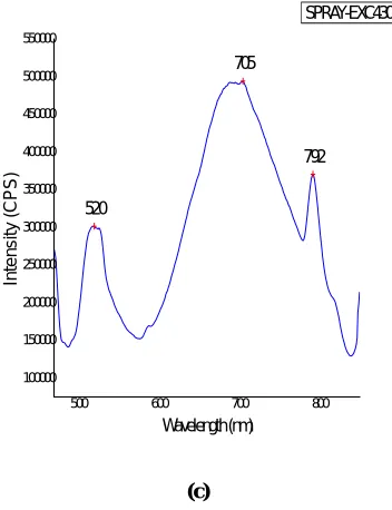
influence on the structure transformation. In CdS thin films, the cadmium vacancies and interstitial sulphur act as acceptors while sulphur vacancies and interstitial cadmium act as donors [19]. The well-known green emission bands at 520,520 and at 524nm are observed in the samples. The enhancement in PL peak at 520,520 and at 524 nm is due to the presence of interstitial sulphur [20, 21]. The main cause of the origin of green emission band is explained as Recombination of free electrons from the conduction band with holes captured on an acceptor level [22]. Recombination of electrons from the donor level with holes trapped on an acceptor level[23]. The PL spectra of the sample (c) shows the broadening of the peak around 520 nm can be attributed to the inhomogeneous in size and the shape of the crystallites. The PL spectra of the samples (a) and (b) clearly depict that the samples have large defect with respect to the concentration and so defects are another cause for the position and broadening of the peak. This indicates formation of the CdS nano particles in the thin film[24]. Depending upon the deposition of the reactants, the films were found to be a polycrystalline in nature. Therefore, in this film the blue shifting of the absorption edge showed that the prepared film is composed of the nanocrystals of the CdS .It is known that the CdS thin film have luminescence in blue , green , red and infra-red region of spectra. The PL could be due to the band edge related to the surface defect state mediated, recombination center in the conventional HOMO-LUMO model [25]. It is well known that the surface defect plays a vital role in the luminescence properties of non-radiative centers. In the films by CBD, SILAR and sprayed, the nanocrystalline increases which causes the increase in the PL intensity at high photo excitation wavelength.
1.0 1.5 2.0 2.5 3.0 3.5
-0.5 0.0 0.5 1.0 1.5 2.0 2.5 3.0 3.5
(h
h
(a)
1.0 1.5 2.0 2.5 3.0 3.5
0.0 0.5 1.0 1.5 2.0 2.5 3.0
h
(h)2
CBD
(b)
1.0 1.5 2.0 2.5 3.0 3.5
-0.2 0.0 0.2 0.4 0.6 0.8 1.0 1.2 1.4
(h
)
2
h
SPRAY PYROLYSIS
(c)
Fig.3. The energy bandgap of CdS thin films grown at different techniques (a) CBD, (b) SILAR and (c) Spray technique
793
500 600 700 800
50000 100000 150000 200000 250000 300000 350000
In
te
n
s
it
y
(
C
P
S
)
Wavelength (nm)
CBD-EXC430-EMM
(a)
792
500 600 700 800
20000 40000 60000 80000 100000 120000 140000 160000
In
te
n
s
it
y
(
C
P
S
)
Wavelength (nm)
SILAR-EXC430-EMM
520
705
792
500 600 700 800
100000 150000 200000 250000 300000 350000 400000 450000 500000 550000
In
te
n
s
it
y
(
C
P
S
)
Wavelength (nm)
SPRAY-EXC430-EMM
[image:4.612.90.266.59.288.2](c)
[image:4.612.66.290.343.383.2]Fig.4. PL spectrum of CdS thin films grown at different techniques (a) CBD, (b) SILAR and (c) Spray technique
Table 1. Thickness and Bandgap measurements for the prepared thin films
Sample Thickness Band Gap(eV) PL Band Gap (eV)
Sample a 5.09 2.25 2.37
Sample b 4.95 2.25 2.37
Sample c 3.2422 2.3 2.38
Structural analysis
The CdS thin films exist in two crystallographic phases namely, greenockite and zin blende respectively. Wurtizite structure is a hexagonal structure and the zinc blende is a cubic structure. The mentioned crystallographic phases of the films are investigated by the X-Ray diffraction patterns. In this present study, the X-Ray diffractrograms of the films prepared by the three techniques are shown in the figure. Some of the data analysis of the structural parameters such as crystallite size, number of crystallite per unit area, defects (strain ) have been calculated from XRD data, listed in the below table. The diffraction patterns of the films were checked against the JCPDS 06-0314 reference pattern [26].
There are two depositional of CdS films during Chemical bath deposition method process
i. Ion-by-ion process (heterogeneous process)
ii. Cluster-by-cluster process (homogeneous process) which results in the pure hexagonal phase or pure cubic phase or mixed cubic-hexagonal phase respectively [27,14].
In this report, the films prepared by CBD and SILAR technique, shows the cubic crystal structure, confirmed by the presence of the planes (220) and (331) associated with this crystallite. Results previously obtained [28] demonstrates the step-by-step formation of the crystalline structure with time duration of 60 minute of deposition, the CdS films show a well-defined cubic structure [29].
The (002) reflections from the XRD for Spray pyrolysis technique shows that the crystallites are more stable hexagonal structure seen at 26.48˚. As the (002) is parallel to the surface of the substrate that is the c-axis is perpendicular to the surface of the substrate. The film prepared by the spray technique have greenockite structure due to the presence of (002), (101), (110), (103), (210) planes. The planes (110) and (101) indicate the covellite phase with the hexagonal crystal structure for the film. In hexagonal structure, each anion is surrounded by four cations at the corners of the tetrahedron and vice versa.
The evaluation of the crystallite size was quantified by using Scherrer’s formula
D = Kλ
βcosθ
Where K is the Scherrer constant λ is the wavelength of the X-ray used
β is the full-width-at- half – maximum (FWHM) of the Bragg reflection under the considerations in radians and θ is the Bragg’s angle was used for the calculation of the crystallite sizes using K= Scherrer’s constant.
The lattice parameters a and c of the unit were evaluated according to this realtion [30]. Using Miller indices of the planes , the lattice parameter a and c of the hexagonal plane are evaluated according to the relation
1
=4(ℎ +ℎ + )
3 +
Where h, k, l are lattice planes and d is the inter plannar spacing determined using Bragg’s equation.
= 2
The dislocation density (δ) has been evaluated from Williamson and Smallman’s formula,
δ= 1
D
The dislocation density measures the quantity of the dislocation present in a material and in the order of 1010 m2 in a sample.
The micro strain (ε) is obtained using the relation
ε=βcosθ
4
Where,
β is the full-width-at-half-maximum; Θ is the bragg’s angle. [31].
The number of crystallites per unit surface area is calculated
N = d
D
Where d is the film thickness;
[image:4.612.135.472.675.717.2]The particle size of the thin films increases with deposition time. [32]. All the structural parameters of the thin films are tabulated in the Table 2. The change of lattice constant indicates that the crystallites were under stress, leading to either elongation or compression of the lattice. This might be due to the change of density and nature of native imperfections with the deposition of the films [33].
Table 2. Comparison of interplanar spacing (d),Grain size (D), Dislocation density( ) Strain(ε), No.of grains per unit area(N)
Sample d value D Ε N Hkl A
Sample a 3.3682 2.9508 1.1484 1.1437 3.2261 111 5.8338
Sample b 2.0580 2.7507 1.3216 1.6459 2.3783 200 5.8209
The decrease in the strain indicates the decrease in the concentration of the lattice imperfections. In the films prepared by the three techniques, the crystal size increase, and which results in decrease in the defects like dislocation density and the strain in the films. . Further a uniform compressive strain (macrostrain) results in peak shift of X-ray diffraction lines. The energy band gap calculations of the films deposited by the three techniques were decreased with increment in the grain size. This decrement in the energy band gap could be attributed to the grain size and dependent grain boundary barrier height [34].
(a)
(b)
(c)
Fig.5. XRD patterns of CdS thin films grown at different techniques (a) CBD, (b) SILAR and (c) Spray technique
Surface Morphology
The surface morphology of the films was observed by the SEM images. Fig 5(a)-(c) shows the SEM images of the samples which do not have any impurities, porosities and structural defects. The distribution of the well-defined grains is not uniform in the samples. The deposited film is made of oblate structure units of 0.5μm and ~250 nm thickness. Quite clearly, excess sulphur in the precursor has promoted the grain growth.From these micrographs, the average grain size was calculated by intercept method using the equation
= 1.5
×
Where m is the magnification of the micrograph, l is the length of the line drawn on the micrograph n is the number of grains crossed by the line and 1.5 is the parameter assuming spherical grains.
The average grain size follows the trend as XRD observation [35].
The Fig.6(a)-(c) shows the SEM images of the CdS thin films prepared by CBD, SILAR and Spray Pyrolysis techniques respectively. It is evident from the SEM images that all the films have homogeneous and smooth surface eventhough there are some stray defective regions. The SEM images depict that the deposition is uniform without pinholes and are polycrystalline in nature. The grain size for the samples (a), (b) and (c) were 100nm, 165nm and 250 nm respectively, it is seen that the top view of the grains are circular in shape. From the figure 6, the surface of the samples is uniform and continuously covered by the material. Also it is noticed that in all the samples, a large density of small number of large grains are scattered on the surface [36]. In the sample (b), the overgrown of the CdS particles were observed. Nevertheless, it was observed from the micrographs that all the samples were homogeneous and without cracks and covered the substrate well. These results are very much agreed with the results of the XRD.
(a)
(c)
Fig.6. SEM micrographs of CdS thin films deposited at different techniques (a) CBD, (b) SILAR, (c) spray technique
Elemental analysis
The EDAX spectra of the CdS samples deposited at different methods shows that all the films contain the elements of Cd and S as expected. They also show other elements (Ca, Na, Si) from the glass substrates. The EDAX revealed the that the presence of Cd:S ratio in the obtained films by CBD and SILAR and Spray pyrolysis, the percentage Cadmium is more than Sulphur ions. The sulphur deficiency can be correlated to the presence of oxygen in the films, because some oxygen ions can be substituted in the sulphur sites in the CdS lattice. A strong peak is observed which corresponds to Si due to substrate. At high operating voltage the electron beam penetrates the film and reaches the glass surface, which results the Si peak. Two different peaks corresponding to Cd and S are found in the spectrum, which confirms the CdS thin film. [37]
(a)
(b)
(c)
Fig.7. EDAX Spectra of CdS thin films deposited at different techniques (a) CBD, (b) SILAR, (c) spray technique
Conclusion
The content of this paper can be summarized by the following statements:
towards the fabrication of the thin films used for the solar cell applications. The optical gap of the material can be controlled by the deposition conditions.
REFERENCES
[1] C.S. Ferekides, D. Marinskiy, V. Viswanathan, B. Tetali, V. Palekis, P. Selvaraj, D.L. Morel, Thin Solid Films
361(362)(2000)520.
[2] J.H. Lee, D.J. Lee, Thin Solid Films515 (2007 )6055 [3] R.A. Berrigan, N. Maung, S.J.C. Irvine, D.J. Cole-Hamilton, D. Ellis, J.Cryst. Growth 195 (1998) 718
[4] G.C. Morris, A. Tottszer, S.K. Das, Mater. Forum 15(1991) 165 [5] J. Hiie, T. Dedova, V.V Aldna, K. Muska. Thin Soilid Films
511(512) (2006)443
[6] O. Savadojo, Sol.Enery matter. Sol.Cells52 (1998) 361 [7] X. Wu, Sol.Energy 77(2004) 803
[8] K. Durose, P.R. Dewards, D.P. Halliday, J.Cryst.Growth 197(199) 733
[9] R. Ortega-Borges,D.LIncot,J.Electrochem.Soc.137(1996) 86 3464
[10] B.R. Lanning ,J.H. Armstrong,Int.J.Sol.Energy 12(1992) 247 [11] A.I,Oliva,R.Castro-Rodriguez,O.Ceh,P.Bartolo-Perez,F.
Caballero-Briones,V.Sosa,Appl.Surf.Sci.148(1992)42 [12] J.M.Dona,J.Herro,J.electrochem,Soc.144 (1997) 4081 [13] J.M.Dona,J.Herro,J.electrochem,Soc.144 (1997) 4091 [14] H.E.Maliki,C.Bernede,S.Marscillac,J.Pinel,X.Castel, J.Pouzet,J.Appl.Surf.Sci.205(2003) 65
[15] Liu,E.K. Zhu, B.S. Luo, J.S.,2008.Semiconductors Physics, Publishing House of electronics industry, Beijing.
[16] Lee, WonjooMin, Sun Ki, Dhas, Vivek Ogale, SatishChandra B,Han-Sung,2009. Chemical bath Deposition of Cds Quantum Dots On vertically aligned Zno nanorods for quantum dots – sentisized solar cells.Electrochem.Commun, 11,103-106. [17] S.M. Pawar, B.S. PAwar, J.H. Kim, Oh-Shim Joo, C.D. Lokhande, Current Applied Physics 11(2011) 117-161 [18] Dabajyot. D and Rantnabali B,1987, thin solid films, vol 147,
p-321
[19] Singh V, Sharma PK, Chauhan P. Surfancant mediated phase transformation of CdSnanoparticles, Mater. ChemPhys 2010; 121; 202-7
[20] Singh V, Chauhan, P.Strucutral and optical characterization of cdS nanoparticles prepared by chemical precipitation method. J.PhysChem Solids 2009; 70:10974-9
[21] Pedrotti LS, Reynolds DC,Change in structure of blue and green fluroscence in cadmium sulphide at low temperatures, Phys Rev 1960; 119;1897
[22] Gracia CM, Esquivel AE, Puente GC, Velazquez MT, Aguilera MLA, Vigil O, et al. Photoluminescence studies of CdS films grown by close-spaced vapor transport hot walls. J. Appl.Phys. 1999; 86:3171-4
[23] Kulp BA, Kelly RH.Displacement of the sulphur atom in CdS by electron Bombardment. J. Appl.phys 1960; 31:1057-61. [24] Manisree manjumder,Aloke Kumar Chakraborty, Biswanath
Mallik; Photoluminescence studies on nano strucutred cadmium sulphide thin films prepared by chemical bath deposition method and annealed at different temperatures; Journal of luminescence, 130 (2010) 1497-1503.
[25] S.Gosh, A.Mukherjee, H.Kim,C.Lee; Mater.Chem.Phys78 (2000) 726
[26] H. Metin, S. Erat, F.M. Emen, V. Kafadar, A.N.Yazici, M.Ari, N.Kulu; The thermo luminescence properties if CdS thin Films under nitrogen atmosphere; Journal of luminescence’130(2010) 1531-1538,Elsevier
[27] K. Ravichandran, P. Philminathan, Appl.Surf.Sci 255 (2009) 5736
[28] R.R. Chamerlain, J.S. Shkarman, J. Electrochem Soc. 137(1966) 86.
[29] A. I. Oliva et al. Applied Surface Science 205(2003) 56-54 [30] B.D. Cullity Elements of X -ray diffraction, Addison-Wesley,
Reading, MA,USA,1977,p.259
[31] K. Girija, S. Thirumumailairajn, S.M. Mohan,; Strctucutral, Morphological And Optical Studies Of Cdse Thin Films From Ammonia Bath, Chalcogenide Letters Vol 6, No 8, August 2009, P 351-357
[32] M. Cao, Y.Sun, J.Wu, X.Chen, N.Dai, Journal of alloys and compounds 508(2010) 297-300
[33] K. Sivaramoorthy, S.AsathBahadur, m.Kottaisamy, K.R. Murali;journal of alloys and compounds 503(2010) 170-176 [34] N.D. Sankir, B. Dogan;Journal of material processing
technology, 211(2011) 382-387
[35] M.A. Barote, A.A. Yadav, L.P. Deshmukh, E.U. Masumdar; Synthesis and characterization of chemically deposited Cd 1-xPbxS thin films; Journal of Non-Oxide Glasses;Vol 2, No 3,
2010,P. 151-165
[36] Shadia J. Ikhmayies, RiyadN. Ahamad-Bitar; Solar energy materials and solar cells 94(2010)878-883
[37] R.K. Sharma, Kiran Jain, A.C. Rastogi, Current applied physics 3 (2003) 199-204