Available Online at www.ijpret.com 761
INTERNATIONAL JOURNAL OF PURE AND
APPLIED RESEARCH IN ENGINEERING AND
TECHNOLOGY
A PATH FOR HORIZING YOUR INNOVATIVE WORK
QUATERNARY ARITHMETIC LOGIC UNIT BASED ON QSD TECHNIQUE
PRAJAKTA V. DESHMUKH, MUKESH D. PATIL
Dept. of Electronics and Telecommunication Engg, SITS, Narhe, Pune-41, Savitribai Phule Pune University Pune, India. Accepted Date: 05/03/2015; Published Date: 01/05/2015
\
Abstract:Interconnects are the ruling contributor to delay, area and energy consumption in CMOS. Multiple-valued logic can reduce the average power and number of interconnections which reduces the overall energy consumption. In this paper, a QLUT (Quaternary Look-Up Table) structure is designed in supersede of binary LUT in FPGA. The circuit is congenial with standard CMOS processes, with one voltage supply and devoting voltage mode structures. A technique used to optimize the switches resistance and power consumption is called as clock boosting. A Quaternary Signed Digit (QSD) number system is used to perform carry free addition, borrow free subtraction and multiplication. A fast Arithmetic Logic Unit (ALU) based on radix 4 system, each improves the computational complexity. Arithmetic operations like addition, multiplication and subtraction in Modulo-4 arithmetic by using multi-valued logic (MVL).
Keywords: Field Programmable Gate Array (FPGA), Quaternary Look-Up Table (QLUT), Multiple Valued-Logic (MVL), Standard CMOS technology, Quaternary Signed Digit (QSD).
Corresponding Author: MS. PRAJAKTA V. DESHMUKH
Access Online On:
www.ijpret.com
How to Cite This Article:
Prajakta V. Deshmukh, IJPRET, 2015; Volume 3 (9): 761-769
Available Online at www.ijpret.com 762 INTRODUCTION
Field Programmable Gate Array (FPGA) has been steadily growing from years. They can be reprogrammed to implement any function, with any amount of parallelism. For million gates FPGA, 90% of area is consumed by interconnects [3]. As interconnects has become preponderant in digital systems, like delay, power and area [4].
(1)
In binary CMOS, static power consumption is closely related to leakage currents, and dynamic power consumption is given by
PD oc CVD D
where C = Capacitance of the nodes driven. VDD = Power Supply Voltage. In CMOS process, contracting of transistors thus reduces C and devoting lower VDD, hence saving power and implementing more functionality into the same area. C also includes routing capacitance related to logic gate wires, where power spent in routing may reach 70% of overall consumption [1]. Multiple-valued logic has been proposed as an alternative to binary logic. As binary logic is limited to only two states, true and false, multiple-valued logic (MVL) supersede these with nite or innite numbers of values [6]. Hence, more information can be carried in each wire, reducing the routing network. Reducing the routing will
(2)
directly reduce the line capacitance and circuit area, which enables the increase in maximum operational frequency and reduction in power consumption. Therefore, the logic gates will come closer and reduce the average power required for level transitions. The new power consumption is
PD O CVD d Vav
where Vav = Average voltage between logic levels [1].
Available Online at www.ijpret.com 763
Organization of paper is as follows: In Section II, gives a basic idea about QLUT and its methodologies and implementations. In Section III, the basic of QSD including the arithmetic logic unit concept. Section IV, concludes with result and discussion.
II. System Implementation
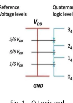
QLUT has four logic levels and three reference voltages i.e. 1/6VDD 3/6VDD, and 5/6VDD to decide quaternary value. Fig.3.1. shows Quaternary variable can carry twice information than binary variable. The group of two binary variables comprises of one
quaternary variable. A LUT is an operator which is array indexing based on configuration memory, where the output is depends on its input. Initially the configuration value is stored in LUT configuration memory, the logic value is assigned to the output according to the input. By programming the memory, the logic function can be implemented on LUT with the given number of input and outputs.
(3)
A quaternary function implemented by a QLUT is defined as g : Q k — Q, over a set of
quaternary input variables Y = (y o, . . . , y ki ), where the values of a variable y i and the function
g(Y ) are defined in Q = 0, 1, 2, 3. In general, if l is the number of logic levels, the total number of different functions | F | that can be implemented in a LUT is given by
| F |= l)nxlk1
k
k
Available Online at www.ijpret.com 764
| F2 |=22k =4
(4)
Where n is the number of outputs and k is the number of inputs. For a LUT with a single output (n = 1), the number of different functions for binary (l = 2) and quaternary (l = 4) representations is given, respectively, by
| F |= 44k = 256
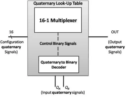
With the same number of inputs and outputs, the number of possible functions that may be represented in a quaternary LUT is much larger than in a binary LUT. Therefore, reducing the total number of connections, MVL also leads to a reduction of the total number of gates[1]. Fig. 3.2. shows two inputs, 16 configuration (reconfigurable quaternary functions) inputs and one output QLUT. There are two main blocks in proposed QLUT: 1) 16-1 multiplexer using array of switches which
Fig. 2. Proposed QLUT
establishes a low resistance path between one configuration input and output according to the input. 2) Quaternary-to-binary Decoder which consist of a 2-bit ADC (Analog-to-Digital converter) and combinational logic used to generate the control signals and given to the multiplexer. These blocks are described in following subsections
Available Online at www.ijpret.com 765
Multiplexer path is made up of transmission gates (TGs) modeled by simple RC circuit. The charging time is proportional to the RC time constant, as the capacitance is constrained; the way to reduce the propagation delay is to reduce the switch resistance. Two methods are used to implement the multiplexer switches: 1. Use of CMOS TGs. 2. Use of single nMOS transistor controlled by the CB circuit. An approach for 2-input QLUT is to employ two series switches in multiplexer. To reduce resistance path and improving the QLUT speed, a single switch is used. This will slightly increase the complexity of decoder and CB circuit to control a single nMOS switch.
B. Clock Boosting Switch
In CB circuit, there are two phases. In phase 1, the capacitor (C) is charged to VDD, and switch (nMOS) is open, as its gate is connected to ground. In phase 2, C is disconnected from VDD, maintaining its charge, while its bottom plate is referred to VDD. Hence, the switch gate voltage becomes 2VDD. In high-level model, the switches are replaced by TGs and depending upon the
clock generator circuit is used to control its phases.
The proposed high-level model. In this, two switches are recognized as an inverter, reducing the number of elements and eliminating the 2-phase clock generator. To delay the signal, this inverter is used and at the same time implementing non-overlapping clock which is used to control the other switches, the capacitor C is initially discharge and clk1 = 1 (VDD), N1 turns ON
and connects node B to GND, while Pi turns OFF and a high impedance path takes place between node A and B. At the same time, P2 is ON and steadily charges the C (and node A) to VDD. When clk1 = 0 (GND), N1 turns OFF, the inverter ties the lower capacitor plate to VDD and P2
turns OFF, node A rises to 2VDD and P1 is turned ON connecting node B to 2VDD as required.
In practice, due to the charge redistribution with transistor Nsw gate capacitance, a small lower voltage is obtained. This small voltage will prevent the transistor for working under a gate voltage close to the maximum voltage (2.7V), avoiding early aging effect on this large transistor. To avoid its compromise towards its long term use, an nMOS in series with N1 is used, avoiding the drain-source voltage to be higher than VDD, in each transistor. A full charge of this capacitor
only once at powering up, from then the capacitor gets discharge due to the charge distribution with switch gate capacitance, it should be noted.
C. Q-B Decoder
Available Online at www.ijpret.com 766
applied in the clk1 input of each switch. These switches are used to connect single configuration input to its output. The quaternary variables are decoded into binary, to generate the control signals, making the use of binary logic gates.
III. QUATERNARY SIGNED DIGIT
In binary number system, carry may propagate through least significant digit to most significant digit. Hence the addition time is depended on word length.
IV. RESULTS AND DISCUSSION
In this paper, an innovative QLUT design is used for multiple valued combinational logic or as a building block in FPGAs. The QLUT internal functionality is implemented using simple standard CMoS structures. This feature is achieved through a quaternary-to-binary decoder that quantizes the input signals. This decoder is based on voltage-mode self-referenced comparators that allow the use of a standard CMoS technology. CB technique was used to decrease the switches resistance and increase the operation frequency, while at the same time, achieving low power consumption. The QSD ALU is better than binary in terms of number of gates used and efficiency will increase with the operation speed.
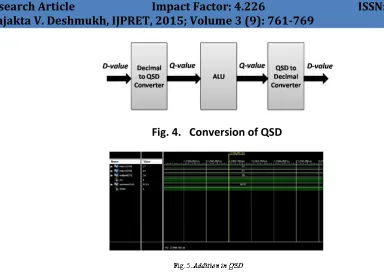
Available Online at www.ijpret.com 767 Fig. 4. Conversion of QSD
In this paper, only the positive side of QSD is taken and negative computations are taken using this positive side. So, the computational range is reduced from -3, -2, -1, 0, 1, 2, 3 to 0, 1, 2, 3 only. This gives 42% improvement in computation complexity and thus increases its efficiency. For example, the original range is of 7 symbols which are reduced to 4 symbols. Thus the computational complexity is (7-4) * (100 / 7) % = 3 * (100 / 7) % = 42% If the decimal value are AD = 35 and BD =28 which are given to the Decimal to QSD converter, as shown in fig. 3.3.
Therefore, AQ = 0 2 0 3 and BQ =0130 then this is given to ALU which will be given to ALU which will perform Addition/Subtraction/Multiplication. If addition is to be done then the two numbers gives 0 3 3 3, then it will again convert QSD into decimal.
0 * (4 3) + 3 * (4 2) + 3 * (4 1) + 3 * (4 0) = 48 + 12 + 3 = 63
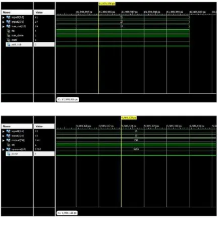
Available Online at www.ijpret.com 768 Fig. 7. Multiplication in QSD
QSD consume 25% less space than BSD to store number. Therefore, the design is a solution to reduce the interconnections impact, without increasing power consumption or losing
Thus we get a decimal value at the output of Q-D converter. Performance and higher number of gates can be tolerated.
REFERENCES
1. Diogo Brito and Taimur G. Rabuske, Student Member, IEEE, Jorge R. Fernandes, Paulo Flores and Jos Monteiro, Senior Member, IEEE, "Quaternary Logic Lookup Table in Standard CMOS" IEEE Transactions On Very Large Scale Integration (VLSI) Systems, February 3, 2014.
2. R.C.G. da Silva, C. Lazzari, H. Boudinov, L. Carro, "CMOS voltage-mode quaternary look-up tables for multi-valued FPGAs", Universidade Federal do Rio Grande do Sul, Brazil, Microelectronics Journal, Re¬ceived 2 April 20 09 Received in revised form 15 July 20 09 Accepted 21 July 20 09, Available online 12 August 2009
Available Online at www.ijpret.com 769
4. Vasundara Patel K S, K S Gurumurthy, "Arithmatic Operations in Multi¬valued Logic", International Journal of VLSI design & Communication Systems (VLSICS), Vol. 1, No. 1, March 2010.
5. Cristiano Lazzari, Paulo Flores, Jos e Monteiro, Luigi Carro, "A New Quaternary FPGA Based on a Voltage-mode Multi-valued Circuit", 978-3-9810801-6-2/DATE10 2010 EDAA
6. Vasundara Patel K S, K S Gurumurthy, "Design of High Performance Quaternary Adders", International Journal of Computer Theory and Engineering, Vol.2, No.6, December, 2010 1793-8201.
7. Diogo Brito, Jorge Fernandes, Paulo Flores, Jos e Monteiro INESC-ID / Instituto Superior T ecnico - TU Lisbon, Portugal, "Design and Characterization of a QLUT in a Standard CMOS Process", 978-1-4673-1260-8/12/$31.00 2012 IEEE
8. Ankita. N. Sakhare, M. L. Keote, "Application of Galois Field in VLSI Using Multi-Valued Logic", International Journal of Engineering Science and Innovative Technology (IJESIT) Volume 2, Issue 1, January 2013, ISSN: 2319-5967, ISO 9001:2008 Certified.