Copyright © 2013 IJECCE, All right reserved 1612
International Journal of Electronics Communication and Computer Engineering Volume 4, Issue 6, ISSN (Online): 2249–071X, ISSN (Print): 2278–4209
Design and Performance Evaluation of Energy Source
for RFID Tag
Gaurav Thakur, Anvay Nandurkar, Rajat Agrawal, Ankita Chauhan
Abstract – This paper presents a rectifying antenna (rectenna) for the harvesting of the microwave energy associated to UHF (Ultra- High Frequency) Radio Frequency Identification (RFID) systems. The proposed device uses a microstrip line monopole with coplanar waveguide feeding line as receiving antenna and a five-stage voltage multiplier as rectifier. Experimental results demonstrating and RF-to-DC conversion efficiency of about 54% with an input power density will be presented and discussed . A compact rectenna circuit at 2.4 GHz is presented. A matching capacitor and five Parallel diodes are introduced to the rectifying circuit so as to achieve well impedance matching. There is a RF-DC conversion efficiency difference of about 3%. The experiment DC output voltage of the rectifying circuit with this novel design achieves 3.0V at a DC load which is a RFID tag. The RF-DC conversion efficiency at desired frequencies could be optimized. Zero bias Schottkey diode model for low RF input power and moderate DC current rectifying antennas (RECTENNAs) is investigated. The model provides diode parameters at the desired output DC current level to be matched with the antenna so that optimum power transfer from antenna to the diode occurs.
Keywords – Rectenna, Radio Frequency, Ultra High Frequency, Radio Frequency Identification, Microstrip Antennas, Microwave EM Energy, Direct Current.
I. I
NTRODUCTIONThe widespread discussion of services and devices using wireless communications has led to a growing interest in electromagnetic (EM) energy harvesting applications. As a consequence, the development of efficient rectifying antennas (rectennas) has become a hot research topic . In fact, a rectenna is a device designed to collect the energy associated to a free propagating EM wave and to transform it into Direct Current (DC) power, thus representing the key element for EM energy harvesting and wireless power transmission applications. A block scheme of the basic architecture of a rectenna is the Radio Frequency (RF)/microwave EM energy is collected by an antenna (the harvester) and converted into DC power by a rectifying circuit (the rectifier). Due to the small amount of energy usually available at the output port of the rectifier in harvesting applications, the load is represented by a low-power device (such as, for instance, a sensor). A rectenna is a RF power receiver that converts the received power into DC power which is consumed by the DC load components, e.g. an active RFID. Rectenna composed of receiving antennas and rectification circuits, is used to transmit microwave power without transmission lines. Rectenna at 2.4 GHz is extensively studied , and rectenna array is also under research . Differently from the single diode, double voltage diode rectifying circuit and the power rectifier circuit , this paper present a novel rectifier operation at 2.4 GHz, combining the double voltage
Copyright © 2013 IJECCE, All right reserved
International Journal of Electronics Communication and Computer Engineering Volume 4, Issue 6, ISSN (Online): 2249–071X, ISSN (Print): 2278–4209
power supply is the most confounding problem. In solving this problem, engineers dusted of a decades-old idea: radio-frequency energy recycling, be it from strategically placed transmitters or from the ambient energy emitted by cellphone towers and television stations. The concept was once dismissed as unfeasible because of the rapid dissipation of electromagnetic waves as they travel from their source. But even microwatts, if trickled into a battery or super capacitor, can be enough to power some sensors1. The use of batteries has two disadvantages
The lifetime of the batteries is very limited even for low-power batteries, requiring impractical periodical battery replacement.
The use of commercial batteries usually overkills the power requirements for uW sensor nodes, adding size and weight while creating the problem of environmental pollution due to the deposition of these batteries, as well as increases significantly the cost overhead of disposable nodes; "being green" is becoming a big requirement in these days; new information and communication technology should be conscious of the energy consumption and effect to the natural environment; in this way solar cells, the most common energy-harvesting technique, cant't soak up photons from inside applications and will be major obstacles for the quick penetration of ubiquitous network services.
A really emerging area is getting hybrid power supplies (solar cells, converting temperature changes or mechanical movements into electrical energy and RF energy recycling) and might finally make the devices truly independent.
II. S
TATE OFA
RTA. Previous Power Transfer Technologies
The development of the microwave tubes during the World War II, rectification of microwave signals for supplying dc power through wireless transmission has been proposed and researched in the context of high power beaming since the 1950s by W. C. Brown who started the modern era of wireless power transmission with the advancement of high-power microwave tubes by Raytheon Company [2]. By 1958, a 15-kW average power-band cross-field amplifying tube was developed that had a measured overall dc to- RF efficiency of 81%. The first receiving device for efficient reception and rectification of microwave power emerged in the early 1960's. Conceived at Raytheon, a rectifying antenna, or rectenna, was developed, consisting of a half-wave dipole antenna with a balanced bridge or single semiconductor diode placed above a reacting plane. The output of the rectenna element is then connected to a resistive load. 2.45 GHz. emerged as the transmitting frequency of choice due to its advanced and efficient technology base, location at the center of an industrial, scientific, and medical (ISM) band, and its minimal attenuation through the atmosphere even in heavy rainstorms, then the conversion efficiency of the rectenna continued to increase from the 1960's through the 1970's this frequency. Based on the Brown's work, P. E. Glaser proposed a Solar Power Satellite (SPS) in 1968[3],
development that was to profoundly afiect the future direction of technology in this area. The SPS is a gigantic satellite designed as an electric power plant orbiting in the Geostationary Earth Orbit (GEO). This consists of mainly three segments; solar energy collector to convert the solar energy into DC (direct current) electricity, DC-to-microwave converter, and large antenna array to beam down the microwave power to the ground.
Conversion efficiency is determined by the amount of microwave power that is converted into dc power by a rectenna element, the greatest conversion efficiency ever recorded by a rectenna element occurred in 1977 by Brown in Raytheon Company using a GaAsPt Schottky barrier diode, a 90.6% conversion efficiency was recorded with an input microwave-power level of 8W. This rectenna element used aluminum bars to construct the dipole and transmission line, Later; a printed thin-film class of rectenna design was developed at 2.45 GHz. where conversion efficiency of 85% were achieved. Another important application for wireless power transmission is to identification tags.
III. B
LOCKD
IAGRAM OFR
ECTENNAFig.1. Block Diagram of Rectenna [1]
A block scheme of the basic architecture of a rectenna is illustrated in Fig. the Radio Frequency (RF)/microwave EM energy is collected by an antenna (the harvester) and converted into DC power by a rectifying circuit (the rectifier). Due to the small amount of energy usually available at the output port of the rectifier in harvesting applications, the load is represented by a low-power device (such as, for instance, a sensor). As highlighted in Fig, in order to improve the rectenna RF-to- DC conversion efficiency two blocks can be added respectively between the antenna and the rectifier and between the rectifier and the load. These blocks act both as filtering and as matching sections; they should be optimized in order to simultaneously fulfil the following functions:
o To match the antenna and the load to the rectifier; o To preserve the antenna from re-irradiating the high
order
o Harmonics generated by the rectifier (to this end the block between
o The antenna and the rectifier should be a pass-band filter);
o To preserve the load from any RF signals (to this end the block
Between the rectifier and the load should be a DC pass filter).
Copyright © 2013 IJECCE, All right reserved
International Journal of Electronics Communication and Computer Engineering Volume 4, Issue 6, ISSN (Online): 2249–071X, ISSN (Print): 2278–4209
power supply is the most confounding problem. In solving this problem, engineers dusted of a decades-old idea: radio-frequency energy recycling, be it from strategically placed transmitters or from the ambient energy emitted by cellphone towers and television stations. The concept was once dismissed as unfeasible because of the rapid dissipation of electromagnetic waves as they travel from their source. But even microwatts, if trickled into a battery or super capacitor, can be enough to power some sensors1. The use of batteries has two disadvantages
The lifetime of the batteries is very limited even for low-power batteries, requiring impractical periodical battery replacement.
The use of commercial batteries usually overkills the power requirements for uW sensor nodes, adding size and weight while creating the problem of environmental pollution due to the deposition of these batteries, as well as increases significantly the cost overhead of disposable nodes; "being green" is becoming a big requirement in these days; new information and communication technology should be conscious of the energy consumption and effect to the natural environment; in this way solar cells, the most common energy-harvesting technique, cant't soak up photons from inside applications and will be major obstacles for the quick penetration of ubiquitous network services.
A really emerging area is getting hybrid power supplies (solar cells, converting temperature changes or mechanical movements into electrical energy and RF energy recycling) and might finally make the devices truly independent.
II. S
TATE OFA
RTA. Previous Power Transfer Technologies
The development of the microwave tubes during the World War II, rectification of microwave signals for supplying dc power through wireless transmission has been proposed and researched in the context of high power beaming since the 1950s by W. C. Brown who started the modern era of wireless power transmission with the advancement of high-power microwave tubes by Raytheon Company [2]. By 1958, a 15-kW average power-band cross-field amplifying tube was developed that had a measured overall dc to- RF efficiency of 81%. The first receiving device for efficient reception and rectification of microwave power emerged in the early 1960's. Conceived at Raytheon, a rectifying antenna, or rectenna, was developed, consisting of a half-wave dipole antenna with a balanced bridge or single semiconductor diode placed above a reacting plane. The output of the rectenna element is then connected to a resistive load. 2.45 GHz. emerged as the transmitting frequency of choice due to its advanced and efficient technology base, location at the center of an industrial, scientific, and medical (ISM) band, and its minimal attenuation through the atmosphere even in heavy rainstorms, then the conversion efficiency of the rectenna continued to increase from the 1960's through the 1970's this frequency. Based on the Brown's work, P. E. Glaser proposed a Solar Power Satellite (SPS) in 1968[3],
development that was to profoundly afiect the future direction of technology in this area. The SPS is a gigantic satellite designed as an electric power plant orbiting in the Geostationary Earth Orbit (GEO). This consists of mainly three segments; solar energy collector to convert the solar energy into DC (direct current) electricity, DC-to-microwave converter, and large antenna array to beam down the microwave power to the ground.
Conversion efficiency is determined by the amount of microwave power that is converted into dc power by a rectenna element, the greatest conversion efficiency ever recorded by a rectenna element occurred in 1977 by Brown in Raytheon Company using a GaAsPt Schottky barrier diode, a 90.6% conversion efficiency was recorded with an input microwave-power level of 8W. This rectenna element used aluminum bars to construct the dipole and transmission line, Later; a printed thin-film class of rectenna design was developed at 2.45 GHz. where conversion efficiency of 85% were achieved. Another important application for wireless power transmission is to identification tags.
III. B
LOCKD
IAGRAM OFR
ECTENNAFig.1. Block Diagram of Rectenna [1]
A block scheme of the basic architecture of a rectenna is illustrated in Fig. the Radio Frequency (RF)/microwave EM energy is collected by an antenna (the harvester) and converted into DC power by a rectifying circuit (the rectifier). Due to the small amount of energy usually available at the output port of the rectifier in harvesting applications, the load is represented by a low-power device (such as, for instance, a sensor). As highlighted in Fig, in order to improve the rectenna RF-to- DC conversion efficiency two blocks can be added respectively between the antenna and the rectifier and between the rectifier and the load. These blocks act both as filtering and as matching sections; they should be optimized in order to simultaneously fulfil the following functions:
o To match the antenna and the load to the rectifier; o To preserve the antenna from re-irradiating the high
order
o Harmonics generated by the rectifier (to this end the block between
o The antenna and the rectifier should be a pass-band filter);
o To preserve the load from any RF signals (to this end the block
Copyright © 2013 IJECCE, All right reserved 1614
International Journal of Electronics Communication and Computer Engineering Volume 4, Issue 6, ISSN (Online): 2249–071X, ISSN (Print): 2278–4209
The rectenna presented was designed to harvest the EM energy associated to UHF (Ultra-High Frequency) Radio Frequency Identification (RFID) systems. The target application could be the powering of low-power sensors in industrial environments. Using UHF RFID systems. Recently, several rectenna devices have been proposed. In particular, rectennas operating in the UHF-RFID band have been proposed . The solution proposed in uses a loop with a meander design as antenna; a conversion efficiency of 4.7% is obtained with an input power of 1mW and a resistive load of 5 k. A rectifying circuit for UHF RFID tag is proposed in conversion efficiency higher than 30%. In a rectenna using a microstrip line antenna is presented on k. Chang, highly efficient c-band circularly polarized rectifying antenna array for wireless microwave power transmission[10]. A conversion efficiency of about 65% with a power density incident on loaded monopole and a five-stage voltage multiplier based on Tikhov, y. I.-j.Song,min, Rectenna design for passive RFID transponders[5]. Varactors were used in designing the matching network between the antenna and the rectifier, thus resulting in the possibility of adjusting the rectenna performance as a function of the signal to be harvested. With respect to the solution presented in, where the antenna and the rectifier must necessarily be on orthogonal planes, the design strategy here proposed allows the positioning of the antenna and of the rectifier on the same plane. Experimental results, referring to a power density incident on the antenna , demonstrate an RF-to-DC conversion efficiency higher than 48% over the entire European UHF RFID band[6].
IV. D
ESIGN OFR
ECTENNAThe design and results of simulations of a single rectenna working at ISM band center in 0.9 GHz and 2.45 GHz. First is presented a brief background about simulation methods used, microstrip antennas and rectifier circuits. As antenna was chosen a microstrip square patch aperture coupled antenna, the design try to have lower dimensions and better polarization bandwidth that a traditional of this kind, this is achieved using a cross-slot in the patch and two feed line each for one polarization, this last to increase the range of incident power; then a dual linear polarization antenna was achieved. As a rectifier was chosen Cockcroft-Walton voltage doubler.
A. Square Patch Microstrip Antenna
A microstrip patch antenna consists of a very thin metallic patch (usually gold) placed a small fraction of a wavelength above a conducting ground plane, separated by a dielectric substrate. Microstrip antennas have numerous advantages, they are light weight, they can be designed to operate over a large range of frequencies (1-40 GHz.), They can easily be combined to form linear or planar arrays, and they can generate linear, dual, and circular polarizations. These antennas are inexpensive to fabricate using printed circuit board etching, which makes them very useful for integrated active antennas in which circuit functions are integrated with the antenna to produce compact Transreceivers. Microstrip antennas can be in
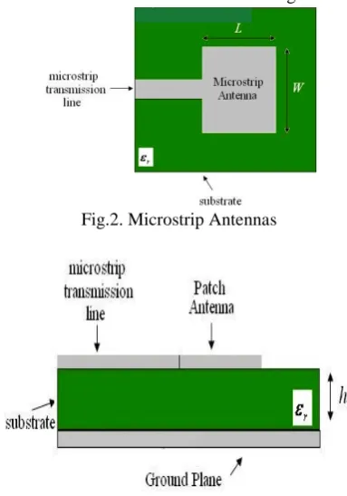
various shapes and configurations but for the purpose of this work only a square patch microstrip antennas are of interest. The basic antenna element is element is based on Seeman K. and R. Weigel, ultra low power rectification in progress [7]. Microstrip or patch antennas are becoming increasingly useful because they can be printed directly onto a circuit board. Microstrip antennas are becoming very widespread within the mobile phone market. Patch antennas are low cost, have a low profile and are easily fabricated. Consider the microstrip antenna shown in Figure , fed by a microstrip transmission line. The patch antenna, microstrip transmission line and ground plane are made of high conductivity metal (typically copper). The patch is of length L, width W, and sitting on top of a substrate (some dielectric circuit board) of thickness h with permittivity Er. The thickness of the ground plane or of the microstrip is not critically important. Typically the height h is much smaller than the wavelength of operation, but not much smaller than 0.05 of a wavelength.
Fig.2. Microstrip Antennas
Fig.3. Square patch microstrip Antenna The center frequency will be approximately given by
Copyright © 2013 IJECCE, All right reserved
International Journal of Electronics Communication and Computer Engineering Volume 4, Issue 6, ISSN (Online): 2249–071X, ISSN (Print): 2278–4209
characteristics of a microstrip patch such as resonant frequency, bandwidth, radiation pattern, etc. The usually used are transmission line model and the cavity model, these models are based on some assumptions, which simplify the calculations at the cost of less accuracy [8]. There are other models that provide more accuracy such as the momentum full-wave model but are also more complicated to analyze. For a given antenna structure the conductors can be broken into "segments", and the currents on the segments can then be determined. The "moment" is numerically the size of vector of current describing the little segment (length and orientation). A set of "basis functions" may be assumed into which the current distributions are decomposed. In the simplest case, the basis functions are rectangular approximations to the Dirac delta function. Because the widths of the rectangular sections are non-zero, only a finite (reasonably small) number of them are needed to cover the antenna structure. The exact Green's functions in spectral domain form are used to find the components from electric and magnetic currents by integrating each slab(there is a mesh of slabs), in general, the "n-th moment" is obtained by integrating the product of the Green's function with the n-th basis function. This Green's function incorporates electrostatic coupling between the moments for the spatial change of the currents.
B. Microstrip Antenna Analytical Models
There are various ways to model a microstrip patch. This modeling is used to predict characteristics of a microstrip patch such as resonant frequency, bandwidth, radiation pattern, etc.The usually used are transmission line model and the cavity model, these models are based on some assumptions, which simplify the calculations at the cost of less accuracy. There are other models that provide more accuracy such as the momemtum full-wave model but are also more complicated to analyze. For a given antenna structure the conductors can be broken into "segments", and the currents on the segments can then be determined. The "moment" is numerically the size of vector of current describing the little segment (length and orientation). A set of "basis functions" may be assumed into which the current distributions are decomposed. In the simplest case, the basis functions are rectangular approximations to the Dirac delta function. Because the widths of the rectangular sections are non-zero, only a nite (reasonably small) number of them are needed to cover the antenna structure. The exact Green's functions in spectral domain form are used to the components from electric "n-th moment" is obtained by integrating "n-the product of "n-the Green's function with the n-th basis function. This Green's function incorporates electrostatic coupling between the moments for the spatial change of the currents. When the current distribution across the antenna structure has been determined, (by integration) is feasible predict characteristics of an antenna. The simulation of the antenna was done using Agilent Momentum method for electromagnetical analysis.
This section addresses the design procedure of an aperture-coupled square patch microstrip antenna in ISM frequencies 2.4-2.5 GHz. whit an input line of 50. Three
Similar antenna structures were designed using different geometric parameters (patch sizes, lengths of aperture coupling, and stub coupling, and insert a second feed line) with the same substrates material. There are two reasons for designing three antennas reduce the dimensions without electing the bandwidth achieved almost at the same cost material; the second and third antenna will be more thick because has a double intermediate Substrates but with less patch size; and to increase the polarization bandwidth. The Two optimum antennas was fabricated and measured for show the improvements and the better was used to integrate the rectifier. These antennas were designed beginning from its basic geometry configuration and then by changing some of this parameters in shape, position and length we success increase the bandwidth; as it is important to receive the greatest possible amount of RF radiation. In its basic configuration a single linearly polarized antennas are expected, with two feed lines properly positioned a dual linear polarization is achieved; this will be discussed in section 3.4 and showed in 3.16, 3.17 and 3.17. There is no exactly step-by-step design procedure for this kind of structure due to the number of interacting design parameters. The following design is a combination of tuning and modelling to arrive at a functional design that meets the above requirements. There is just one point to start with the modelling and tuning: is necessary a basic dimensions, this and design process are discussed in the following sections.[4]
V. F
ABRICATIONThe last two designed antennas: (1) optimized size and (2) optimized size and bandwidth, circuit pads, one branch rectifier, complete rectifier with to branches and integrated rectenna were fabricated in the \CTTC design laboratory".
1. All data from Agilent ADS momentum simulation is exported to LPKF milling machine software.
2. The A25N substrate (for front and back side of our antenna) into the work surface of LPKF milling machine in which the shadows of the patch and pads over the copper are marked, ground vias holes made and substrate cut at the ground plane size. Unfortunately at the mill over the patch was to depth and was necessary a second try.
3. The unwanted copper is removed by hand using a cutter and following the marks made by the machine.
4. The two Rohacell51 foams were easily cut by hand with a cutter
5. The back side A25N substrate is cover with a paste and inserted into a chamber in which is heated to metalize the ground via holes and connect these with the ground plane.
6. After each layer is properly milled and cut the inductors, capacitor and resistor are soldered in the back side of the antenna under the ground plane side, over the pads and ground vias designed . In the separately antenna and branches rectifier cases a SMA connectors are soldered to each port .
Copyright © 2013 IJECCE, All right reserved 1616
International Journal of Electronics Communication and Computer Engineering Volume 4, Issue 6, ISSN (Online): 2249–071X, ISSN (Print): 2278–4209
fabrication process for an integrated rectenna where the antenna is over the top layer and rectifier under the bottom layer due to the structure of the microstrip aperture coupled antennas allowed.[9][11]
VI. M
EASUREMENTSFour sets of measurements will be made on: The optimized size antenna, the optimized size and polarization antenna, one branch rectifier circuit and the integrated rectenna. Antennas were tested for S11 parameters and radiation patterns; one branch rectifier circuit also was tested for their S11 parameters and RF-DC conversion efficiency as a function of frequency and input power, and the integrated rectenna for its RF-DC conversion efficiency as a function of frequency, incident power and polarization mismatch.
A. Measurement Setup and Limitations
Antennas measurements: Antennas were tested for its return losses and radiation patterns; the return losses was measured in a Rohde & Schwarz ZVA24 vector network analyzer with the properly calibration for S11 measure. In the patterns radiation cases, measurements were taken in a walk-in anechoic chamber. The transmission antenna was an open boundary quadridge horn model specified for use from 2 to 18 GHz. The receiving antenna was the antenna under test AUT, i.e. were three ATUs, the optimized size antenna, the optimized size and polarization bandwidth antenna and the integrated rectenna, the same antenna that case but now with the rectifier circuit builded behind. One branch rectifier measurements and efficiency was measured generating two kinds of input signal with a Agilent E4438C vector signal generator: A single frequency signal (without modulation) with a 802.11b signal,(11Mbps, QPSK modulation, each channel of 22MHz with 11MHz of -3dB bandwidth) in the three European non overlapping channels like RF input; and in the DC output was connected an Digital Multimeter. Rectenna efficiency measurement In the case of the integrated rectenna measurements each data-point consists of at least a DC voltage, i.e. the DC output of the rectenna, and was taken versus at least one of the following variables: transmitted power Pt, frequency ,elevation angle or azimuth angle '.Fig,shows the measurement setup.
VII. V
OLTAGED
OUBLER ORR
ECTIFIER.
A basic schematic of a Villard voltage doubler, sometimes also called Cockcroft-Walton voltage multiplier [6]. A DC voltage of twice the peak amplitude of the input AC signal can be generated at the DC output. And ideally, arbitrary output DC voltage can be reached by building cascaded stages of the doubler, figure. In the real case, the amplitude of the AC signal will be divided by coupling capacitors and the junction capacitance of the diode. Also the reverse leakage current of the diode and the resistance of the diode will limit the feasible DC output. Therefore, to obtain the maximum voltage, large coupling and charge-storage capacitance is preferred.
Fig.4. Voltage doubler circuit
In addition, larger capacitance stores more energy and consequently provides more current when discharging. Low series resistance Schottky diodes are most suitable for implementing the circuit due to its high forward bias current for a given voltage. According to the analysis above, the junction capacitance should be minimized to achieve higher output voltage, then this is the main condition to properly choice of diode. The equivalent input impedance of the rectifiers is decided by the diode junction capacitance, which is much smaller than the serially connected coupling and storage capacitance. By other hand, like in transformers, when voltage is stepped up, the output current decreases. This is also true of voltage multipliers. Although the measured output voltage of a voltage multiplier may be several times greater than the input voltage, once a load is connected the value of the output voltage decreases. Also any small uctuation of load impedance causes a large actuation in the output voltage of the multiplier. For this reason, voltage multipliers are used only in special applications where the load is constant and has a high impedance or where input voltage stability is not critical. The rectifier is a five stage Cockcroft-Walton voltage multiplier . Diodes are the HSMS-285C by Avago Technologies, while capacitors are 251R15 (0805) S-series by Johanson. The presence of a 10 microfarad DC pass capacitor can be also noticed. A double-sided copper clad FR4 laminate (Er = 3:7, h = 1:6mm) was used for fabrication.
A. Construction
Fig.5. Metal semiconductor junction & symbol of schottky diode.
A metal–semiconductor junction is formed between a metal and a semiconductor, creating a Schottky barrier (instead of a semiconductor–semiconductor junction as in conventional diodes). Typical metals used are molybdenum, platinum, chromium or tungsten, and certain Copyright © 2013 IJECCE, All right reserved
1616
International Journal of Electronics Communication and Computer Engineering Volume 4, Issue 6, ISSN (Online): 2249–071X, ISSN (Print): 2278–4209
fabrication process for an integrated rectenna where the antenna is over the top layer and rectifier under the bottom layer due to the structure of the microstrip aperture coupled antennas allowed.[9][11]
VI. M
EASUREMENTSFour sets of measurements will be made on: The optimized size antenna, the optimized size and polarization antenna, one branch rectifier circuit and the integrated rectenna. Antennas were tested for S11 parameters and radiation patterns; one branch rectifier circuit also was tested for their S11 parameters and RF-DC conversion efficiency as a function of frequency and input power, and the integrated rectenna for its RF-DC conversion efficiency as a function of frequency, incident power and polarization mismatch.
A. Measurement Setup and Limitations
Antennas measurements: Antennas were tested for its return losses and radiation patterns; the return losses was measured in a Rohde & Schwarz ZVA24 vector network analyzer with the properly calibration for S11 measure. In the patterns radiation cases, measurements were taken in a walk-in anechoic chamber. The transmission antenna was an open boundary quadridge horn model specified for use from 2 to 18 GHz. The receiving antenna was the antenna under test AUT, i.e. were three ATUs, the optimized size antenna, the optimized size and polarization bandwidth antenna and the integrated rectenna, the same antenna that case but now with the rectifier circuit builded behind. One branch rectifier measurements and efficiency was measured generating two kinds of input signal with a Agilent E4438C vector signal generator: A single frequency signal (without modulation) with a 802.11b signal,(11Mbps, QPSK modulation, each channel of 22MHz with 11MHz of -3dB bandwidth) in the three European non overlapping channels like RF input; and in the DC output was connected an Digital Multimeter. Rectenna efficiency measurement In the case of the integrated rectenna measurements each data-point consists of at least a DC voltage, i.e. the DC output of the rectenna, and was taken versus at least one of the following variables: transmitted power Pt, frequency ,elevation angle or azimuth angle '.Fig,shows the measurement setup.
VII. V
OLTAGED
OUBLER ORR
ECTIFIER.
A basic schematic of a Villard voltage doubler, sometimes also called Cockcroft-Walton voltage multiplier [6]. A DC voltage of twice the peak amplitude of the input AC signal can be generated at the DC output. And ideally, arbitrary output DC voltage can be reached by building cascaded stages of the doubler, figure. In the real case, the amplitude of the AC signal will be divided by coupling capacitors and the junction capacitance of the diode. Also the reverse leakage current of the diode and the resistance of the diode will limit the feasible DC output. Therefore, to obtain the maximum voltage, large coupling and charge-storage capacitance is preferred.
Fig.4. Voltage doubler circuit
In addition, larger capacitance stores more energy and consequently provides more current when discharging. Low series resistance Schottky diodes are most suitable for implementing the circuit due to its high forward bias current for a given voltage. According to the analysis above, the junction capacitance should be minimized to achieve higher output voltage, then this is the main condition to properly choice of diode. The equivalent input impedance of the rectifiers is decided by the diode junction capacitance, which is much smaller than the serially connected coupling and storage capacitance. By other hand, like in transformers, when voltage is stepped up, the output current decreases. This is also true of voltage multipliers. Although the measured output voltage of a voltage multiplier may be several times greater than the input voltage, once a load is connected the value of the output voltage decreases. Also any small uctuation of load impedance causes a large actuation in the output voltage of the multiplier. For this reason, voltage multipliers are used only in special applications where the load is constant and has a high impedance or where input voltage stability is not critical. The rectifier is a five stage Cockcroft-Walton voltage multiplier . Diodes are the HSMS-285C by Avago Technologies, while capacitors are 251R15 (0805) S-series by Johanson. The presence of a 10 microfarad DC pass capacitor can be also noticed. A double-sided copper clad FR4 laminate (Er = 3:7, h = 1:6mm) was used for fabrication.
A. Construction
Fig.5. Metal semiconductor junction & symbol of schottky diode.
Copyright © 2013 IJECCE, All right reserved
International Journal of Electronics Communication and Computer Engineering Volume 4, Issue 6, ISSN (Online): 2249–071X, ISSN (Print): 2278–4209
silicides, e.g. palladium silicide and platinum silicide; and the semiconductor would typically be n-type silicon.[1] The metal side acts as the anode and n-type semiconductor acts as the cathode of the diode. This Schottky barrier results in both very fast switching and low forward voltage drop. The choice of the combination of the metal and semiconductor determines the forward voltage of the diode. Both n- and p-type semiconductors show the Schottky effect; the p-type has typically much lower forward voltage. As the reverse leakage current increases dramatically with lowering the forward voltage, it can not be too low; the usually employed range is about 0.5–0.7 V and p-type semiconductors are employed only rarely. Titanium silicide and other refractory silicides, which are able to withstand the temperatures needed for source/drain annealing in CMOS processes, usually have too low forward voltage to be useful; processes using these silicides therefore usually do not offer Schottky diodes. With increased doping level of the semiconductor the width of the depletion region drops. Below certain width the charge carriers can tunnel through the depletion region. At very high doping levels the junction does not behave as a rectifier anymore and becomes an ohmic contact. This can be used for simultaneous formation of ohmic contacts and diodes, as diodes form between the silicide and lightly doped n-type region and ohmic contacts form between the silicide and a heavily doped n- or p-type region. Lightly doped P regions pose a problem as the resulting contact has too high resistance for a good ohmic contact and too low forward voltage and too high reverse leakage to be a good diode. As the edges of the Schottky contact are fairly sharp, high electric field gradient occurs around them which limits the reverse breakdown voltage. Various strategies are used, from guard rings to overlaps of metallization to spread out the field gradient. The guard rings consume valuable die area and are used primarily for large higher-voltage diodes, while overlapping metallization is employed primarily with smaller, low-voltage diodes. Schottky diodes are often used as antisaturation clamps on transistors. Palladium silicide ones are excellent here due to their lower forward voltage (which has to be lower than the forward voltage of the base-collector junction); platinum silicide ones have forward voltage closer to that and require more attention in layout. The Schottky temperature coefficient is lower than the coefficient of the B–C junction, which limits the use of PtSi at higher temperatures .For power schottky diodes the parasitic resistances of the buried N+ layer and the epitaxial n-type layer become important. The resistance of the epitaxial layer is more important here than for a transistor as the current has to cross its entire thickness. It however serves as a distributed ballasting resistor over the entire area of the junction and prevents localized thermal runaway under usual conditions. In comparison with the power p–n diodes the Schottky diodes are less rugged. The junction lies in direct contact to the thermally sensitive metallization, a Schottky diode can therefore dissipate less power than an equivalent size p–n one with deep-buried junction, before failing - especially during reverse breakdown.
B. Normal P-N Doide vs Zero Bais Schottkey Diode
Fig.6. Comparision characteristics of p-n junction diode & schottkey diode
Normal P-N junction cant be use in voltage multiplier. Voltage multiplier uses zero bais schotky diodes.A DC pass capacitor is use to preserve the load from unwanted AC signals and to improve the RF-to-DC conversion efficiency. With increased doping level of the semiconductor the width of the depletion region drops. Below certain width the charge carriers can tunnel through the depletion region. At very high doping levels the junction does not behave as a rectifier anymore and becomes an ohmic contact. This can be used for simultaneous formation of ohmic contacts and diodes, as diodes form between the silicide and lightly doped n-type region and ohmic contacts form between the silicide and a heavily doped n- or p-type region. Lightly doped P regions pose a problem as the resulting contact has too high resistance for a good ohmic contact and too low forward voltage and too high reverse leakage to be a good diode. As the reverse leakage current increases dramatically with lowering the forward voltage, it can not be too low; the usually employed range is about 0.5–0.7 V and p-type semiconductors are employed only rarely.
VIII. S
UPERC
APACITORFig.7. Diagram of supercapacitor
Batteries have been the preferred storage device for most applications because of their superior capability to store energy (i.e. high energy density). But batteries are limited in their ability to deliver power—they can store lots of energy but take a long time to discharge or recharge. Where the application has demanded high power, batteries have been over engineered and the lifetime of the battery compromised. New battery technology such as lithium ion has been developed to increase power and energy storage. Fundamentally, however, they are energy storage devices [8].
As such batteries will always be a poor solution where high power is required. Because of this, mature battery and capacitor technologies are unlikely to be able to meet the needs of today's wireless, power-hungry technologies. Supercapacitors, however, offer a unique combination of Copyright © 2013 IJECCE, All right reserved
International Journal of Electronics Communication and Computer Engineering Volume 4, Issue 6, ISSN (Online): 2249–071X, ISSN (Print): 2278–4209
silicides, e.g. palladium silicide and platinum silicide; and the semiconductor would typically be n-type silicon.[1] The metal side acts as the anode and n-type semiconductor acts as the cathode of the diode. This Schottky barrier results in both very fast switching and low forward voltage drop. The choice of the combination of the metal and semiconductor determines the forward voltage of the diode. Both n- and p-type semiconductors show the Schottky effect; the p-type has typically much lower forward voltage. As the reverse leakage current increases dramatically with lowering the forward voltage, it can not be too low; the usually employed range is about 0.5–0.7 V and p-type semiconductors are employed only rarely. Titanium silicide and other refractory silicides, which are able to withstand the temperatures needed for source/drain annealing in CMOS processes, usually have too low forward voltage to be useful; processes using these silicides therefore usually do not offer Schottky diodes. With increased doping level of the semiconductor the width of the depletion region drops. Below certain width the charge carriers can tunnel through the depletion region. At very high doping levels the junction does not behave as a rectifier anymore and becomes an ohmic contact. This can be used for simultaneous formation of ohmic contacts and diodes, as diodes form between the silicide and lightly doped n-type region and ohmic contacts form between the silicide and a heavily doped n- or p-type region. Lightly doped P regions pose a problem as the resulting contact has too high resistance for a good ohmic contact and too low forward voltage and too high reverse leakage to be a good diode. As the edges of the Schottky contact are fairly sharp, high electric field gradient occurs around them which limits the reverse breakdown voltage. Various strategies are used, from guard rings to overlaps of metallization to spread out the field gradient. The guard rings consume valuable die area and are used primarily for large higher-voltage diodes, while overlapping metallization is employed primarily with smaller, low-voltage diodes. Schottky diodes are often used as antisaturation clamps on transistors. Palladium silicide ones are excellent here due to their lower forward voltage (which has to be lower than the forward voltage of the base-collector junction); platinum silicide ones have forward voltage closer to that and require more attention in layout. The Schottky temperature coefficient is lower than the coefficient of the B–C junction, which limits the use of PtSi at higher temperatures .For power schottky diodes the parasitic resistances of the buried N+ layer and the epitaxial n-type layer become important. The resistance of the epitaxial layer is more important here than for a transistor as the current has to cross its entire thickness. It however serves as a distributed ballasting resistor over the entire area of the junction and prevents localized thermal runaway under usual conditions. In comparison with the power p–n diodes the Schottky diodes are less rugged. The junction lies in direct contact to the thermally sensitive metallization, a Schottky diode can therefore dissipate less power than an equivalent size p–n one with deep-buried junction, before failing - especially during reverse breakdown.
B. Normal P-N Doide vs Zero Bais Schottkey Diode
Fig.6. Comparision characteristics of p-n junction diode & schottkey diode
Normal P-N junction cant be use in voltage multiplier. Voltage multiplier uses zero bais schotky diodes.A DC pass capacitor is use to preserve the load from unwanted AC signals and to improve the RF-to-DC conversion efficiency. With increased doping level of the semiconductor the width of the depletion region drops. Below certain width the charge carriers can tunnel through the depletion region. At very high doping levels the junction does not behave as a rectifier anymore and becomes an ohmic contact. This can be used for simultaneous formation of ohmic contacts and diodes, as diodes form between the silicide and lightly doped n-type region and ohmic contacts form between the silicide and a heavily doped n- or p-type region. Lightly doped P regions pose a problem as the resulting contact has too high resistance for a good ohmic contact and too low forward voltage and too high reverse leakage to be a good diode. As the reverse leakage current increases dramatically with lowering the forward voltage, it can not be too low; the usually employed range is about 0.5–0.7 V and p-type semiconductors are employed only rarely.
VIII. S
UPERC
APACITORFig.7. Diagram of supercapacitor
Batteries have been the preferred storage device for most applications because of their superior capability to store energy (i.e. high energy density). But batteries are limited in their ability to deliver power—they can store lots of energy but take a long time to discharge or recharge. Where the application has demanded high power, batteries have been over engineered and the lifetime of the battery compromised. New battery technology such as lithium ion has been developed to increase power and energy storage. Fundamentally, however, they are energy storage devices [8].
Copyright © 2013 IJECCE, All right reserved 1618
International Journal of Electronics Communication and Computer Engineering Volume 4, Issue 6, ISSN (Online): 2249–071X, ISSN (Print): 2278–4209
high power and high energy performance parameters with commercial relevance.
Battery-free devices are one of the emerging applications for supercapacitors. They consist of low power energy harvesters that supply power, while the supercapacitors store the energy and provide the high current pulses. Energy harvesting combined with energy storage can achieve extended life span, and eliminate the need for battery replacements in WSN (Wireless Sensor Networks).
Fig.8. Double layer capacitors
Electrochemical Double Layer Capacitors (EDLCs) – also called supercapacitors (SC) - are electrochemical capacitors that have high capacitance and high energy density when compared to common capacitors, and higher power density when compared to batteries.
A. Advantages of supercapacitor
Long life timeLittle degradation over hundreds of thousands of cycles Not subject to the wear and aging experienced by electro-chemical batteries
Low impedance (ESR)
Enhances pulse current handling by parallel connection with an electro-chemical battery
Rapid charging and discharging
Low-impedance super capacitors charge in seconds (in contrast to secondary batteries)
Simple charge methods
No full-charge detection is needed; no danger of overcharge
Cost-effective energy storage Low cost per cycle
Lower energy density compensated by a very high cycle count
One supercapacitor can replace many regular capacitors
Reduces voltage drop compared to battery operated device with no SuperCapacitor
Infinite charging cycles versus secondary battery Extended operation temperature range
Allows use of batteries at very low temperatures No chemical reaction occurs on the electrodes
Much slower ageing and degradation compared to batteries
Low heating levels
Meets environmental standards Improved safety
Supercapacitors do not explode even if overcharged.[3][5][12]
IX. A
PPLICATIONS Wildlife management.
Supermarket for automatic billing. Detection of earthquake.
Traffic and life monitoring of bridges.
School\College\offices Badges for automatic attendance.
Tourists monitoring.
Vehicle Tires for pressure and temperature monitoring. Automobile during production can be used to track its
progress.
Pharmaceuticals can be tracked through warehouses and many other applications.[13]
X. A
DVANTAGE Greater range of detection (up to 100 meters). Better noise immunity.
Effective with less powerful readers. High data transmission rate.
More tags can be read simultaneously. Less orientation sensitivity.
Read/Write memory capability.
XI. R
ESULT& C
ONCLUSIONCopyright © 2013 IJECCE, All right reserved
International Journal of Electronics Communication and Computer Engineering Volume 4, Issue 6, ISSN (Online): 2249–071X, ISSN (Print): 2278–4209
R
EFERENCES[1] Takhedmit, H., et al., \A 2.45-GHz low cost and e±cient
rectenna," Proc. of the 4th EuCAP, Barcelona, Spain, Apr. 2010.
[2] Monti, G., L. Tarricone, and M. Spartano, \X-band planar
rectenna," Antenn. and Wirel. Propag. Lett., Vol. 10,
1116{1119,2011}
[3] Heikkinen, J. and M. Kivikoski, \Low-pro¯ le circularly polarized
rectifying antenna for wireless power transmission at 5.8 GHz,"
IEEE Microw. and Wirel. Compon. Lett., Vol. 14, No. 4 Apr.
2004.
[4] Chen, R. H., Y. C. Lee, and J. S. Sun, \Design and experiment of
a rectifying antenna for 900MHz wireless power transmission,"
PIERS Proceedings, Beijing, China, Mar. 2009.
[5] Seeman, K. and R. Weigel, \Ultra low power recti¯ cation in
Progress In Electromagnetics Research C, Vol. 31, 2012 121 passive RFID tags at UHF frequencies," Frequenz, No. 59, 112{115, 2005.}
[6] Rizzoli, V., G. Bichicchi, A. Costanzo, F. Donzelli, and D.
Masotti, \CAD of multi-resonator rectenna for micro-power generation," Proc. of the 4th EuMIC, Rome, Italy, Sep. 2009.
[7] Congedo, F., G. Monti, and L. Tarricone, \Broadband bowtie
antenna for RF energy scavenging applications," Proc. of 4th EuCAP, 11{15, Rome, Apr. 2011.
[8] Johanson technology, R15S (0805) S-Series, Low ESR
Capacitor Multi-Layer High-Q data sheet, retrieved in June 2012, from www.johansontechnology.com/.
[9] Agilent, Advanced Design System brochure, retrivied in June
2012, from www.agilent.com/¯ nd/eesof-ads.
[10] Computer Simulation Technology, www.cst.com/ [visited on
June 30, 2012].
[11] Murata Europe, www.murata.eu/.
[12] gnuradio.org/ [visited on June 30, 2012].
[13] Ettus Research LLC, RFX-900 daughterboard product details,