Published online September 30, 2014 (http://www.sciencepublishinggroup.com/j/ajpc) doi: 10.11648/j.ajpc.20140304.12
ISSN: 2327-2430 (Print); ISSN: 2327-2449 (Online)
First-principles calculations of the formation and
structures of point defects on GaN (0001) surface
Chun Yang
1, Weiwei Jie
2, Ping Huang
2, Xiaoqing Liang
1, Xiaoxiao Pan
11
College of Chemistry and Materials, Sichuan Normal University, Chendu, China
2
College of Physics and Electronic Engineering, Sichuan Normal University, Chendu, China
Email address:
[email protected] (Chun Yang)
To cite this article:
Chun Yang, Weiwei Jie, Ping Huang, Xiaoqing Liang, Xiaoxiao Pan. First-Principles Calculations of the Formation and Structures of Point Defects on GaN (0001) Surface. American Journal of Physical Chemistry. Vol. 3, No. 4, 2014, pp. 47-53.
doi: 10.11648/j.ajpc.20140304.12
Abstract:
We studied the structures and energies associated with 8 types of point defects on the [0001] surface of hexagonal gallium nitride (GaN) by modeling: (1) Ga vacancies (VGa), (2) N vacancies (VN), (3) substitution of N by Ga (GaN), (4) substitution of Ga by N (NGa), (5) Ga octahedral interstitial defects (GaO), (6) Ga tetrahedral interstitial defects (GaT), (7) N octahedral interstitial defects (NO), and (8) N tetrahedral interstitial defects (NT). Using a plane-wave ultrasoft pseudopotential method, we calculate these defect structures, simulate the shift, bonding, and relaxation reconstruction of surface atoms in response to the formation of these defects and also calculate the formation energies of these defects. We find that the Ga-related defects only slightly affect the surface, whereas all N-related defects induce substantial surface reconstruction. In particular, the formation of NT not only induces distortion of the surface structure, but also significantly influences the structure of the deeper lattice space. Calculations of formation energies suggest that, in Ga-rich conditions, GaO forms most easily, followed by GaN, VN, and GaT. In comparison, in N-rich conditions, VGa forms most easily. In all environments, GaO, GaN, and VGa form more easily than VN, and the formation of octahedral interstitial defects requires less energy than tetrahedral interstitial defects, which suggests it is difficult to form tetrahedral interstitial defects in the GaN (0001) surface.Keywords:
Point Defect, Gallium Nitride, Surface Reconstruction, Simulation1. Introduction
Gallium nitride (GaN) is a promising material for high-frequency and high-temperature devices because of its wide band gap (3.4 eV), high breakdown voltage (4 MV/cm), and high electron saturation velocity (3×107 cm/s). Heterostructures based on the surface growth of oxides on GaN are used in various applications, such as high-efficiency blue and green light-emitting devices,
ultraviolet light-emitting diodes,
metal-oxide-semiconductor field-effect transistors, and gallium nitride/aluminum gallium nitride heterostructure field-effect transistors [1–3].
It is generally easy to prepare GaN (0001) surfaces, but variations in conditions during
crystal growth can result in imperfections in the (0001) surface, such as native point defects, line defects, dislocations, and (1×1), (2×2), (4×4), (5×5), and (6×4)
constructions [4–7]. These defects can interact with charge carriers during device operation and lead to deterioration of their performance.
Theoretical modeling of crystal surfaces can reveal the microscopic structure and properties of the surface electrons, and, thus, provide insights that cannot be obtained experimentally. For example, plane-wave ultrasoft pseudopotential methods based on first principles have been successfully used to study the atomic and electronic structure of material surfaces [8, 9]. In this study, we used this reliable method to analyze point defects on the GaN (0001) surface and investigate their formation and stability.
2. Physical Model and Calculation
Methods
Fig 1. Model of ideal GaN (0001) slab containing eight atomic layers.(a)
side face(b)planform Ga; N; H
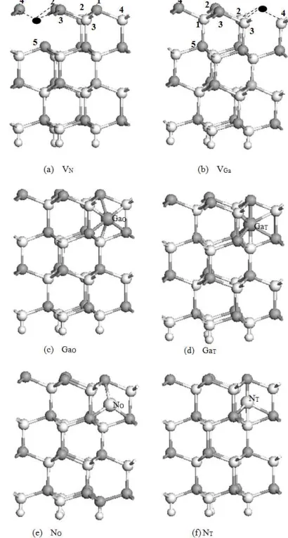
Fig 2. (a), (b) Top views of GaN (0001) surfaces containing vacancies, substitutions, and Ga interstitial defects; (c), (d) larger atoms represent substituting atoms; (e), (f) larger grey atoms represent interstitial atoms
Ga; N; H
We constructed and structurally optimized an ideal semi-infinite GaN slab with a (0001) surface and then introduced various native defects in the surface. The atoms at the bottom surface of the slab were saturated with hydrogen to passivate the dangling bonds. The H–N bond length was set at 0.102 nm, consistent with the length in ammonia. A 1-nm vacuum thickness was chosen to ensure that interactions between the top and bottom surfaces of the slab could be ignored. The GaN (0001) surface (i.e. the outermost surface of the GaN slab) was Ga terminated. To
reduce the calculation load, the model contained eight atomic layers and (2×2) surface supercells were created along the [0001] direction (see Fig. 1).
Eight types of surface point defects were created based on the results of previous studies [10–13]: (1) Ga vacancies (VGa), (2) N vacancies (VN), (3) Ga tetrahedral interstitial atoms (GaT) located midpoint on the c axis between the nonbonded Ga and N and surrounded by the two nearest neighbor atoms and six second-nearest neighbor atoms, (4) Ga octahedral interstitial atoms (GaO) located on the c axis at the center of the hexagonal channel between Ga and N layers and surrounded by three nearest neighbor atoms: 3 N and 3 Ga atoms, (5) substitution of an N1 by a Ga (GaN), (6) substitution of a Ga1 by a N (NGa), (7) N tetrahedral interstitial atoms (NT) positioned similar to GaT, and (8) N octahedral interstitial atoms (NO) positioned similar to GaO. The models are illustrated in Figs. 2 and 3. To reduce the required calculation time, the supercell lattice parameters were fixed and relaxation optimization was allowed only in the five outermost atomic layers.
Fig 3. Side views of GaN (0001) surface containing vacancies and interstitial defects. (a) (b) show the vacancies of N and Ga; (c) ,(d), (e) and (f) are the interstitial defects of GaO ,GaT; NO; and NT respectively
A plane-wave ultrasoft pseudopotential method based on density functional theory was used for the calculations. In the method, the actual ion potentials were replaced by their pseudopotentials, and the wave functions were expanded using plane-wave basis sets. The generalized-gradient approximation formulated by Perdew and Wang (PW91) was used for the exchange-correlation energy[14] and spin-polarization effects were taken into account. The geometrical parameters of the GaN lattice calculated with this scheme (Table 1) are closer to the experimentally determined values than those calculated using the PBE [15] and PRBE schemes [16]. In our calculations, the Ga 3d104s24p1 electrons and the N 2s22p3 electrons were treated as valence electrons. The plane-wave cutoff energy (Ecut)
was chosen as 408 eV. Brillouin integration was performed through the summation of 16 special K points over the Brillouin zone. Self-consistency was achieved using the Pulay density mixing scheme with the self-consistency precision set at 2.0×10⁻⁶ eV/atom. Geometric optimization was performed by the BFGS algorithm [17]. To reduce the calculation time, the condition for the convergence of interatomic interactions was chosen as 0.5 eV/nm. All calculations were performed assuming electrically neutral systems.
3. Results and Discussion
3.1. Geometric Configuration of Surface Atoms
Table 1. Geometric parameters of GaN structure and cohesive energy used in calculations
Document a (nm) c(nm) c/a u Ecoh cohesion(eV)
Our Calculation 0.3205 0.5219 1.628 0.376 - 9.91
Document [16] 0.3206 0.5220 1.628 0.377 -8.21
Document [17] 0.3224 0.5246 1.627 0.377 -9.15
Experiment [19] 0.3158 0.5185 1.626 0.375 -9.06
Table 2. Mulliken charge on atoms surrounding surface vacancies and relaxation of surrounding atoms induced by vacancies. The [0001] direction is regarded as positive and the [001] direction is regarded as negative. Units are nm
Surface Ga1 Ga2 Ga3 Ga4 N1 N2 N3 N4
Perfect 0.71 0.71 0.71 0.71 -0.98 -0.98 -0.98 -0.98
VGa
0.90 -0.0021
0.90 -0.0021
0.89 -0.0021
-1.04 0.0001
-1.00 0.0001
-1.00 0.0001
-1.00 0.0001
VN
0.78 -0.002
0.33 -0.0002
0.33 -0.0002
0.33 -0.0002
-0.95 0.0003
-0.95 0.0003
-0.95 0.0002
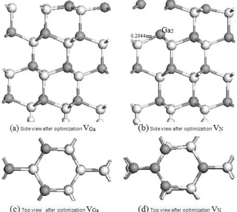
Table 1 summarizes the relaxation of the adjacent atoms in response to the formation of surface-vacancy defects. A VGa defect induces only a moderate relaxation of 0.0001 nm in the [0001] direction. However, the three Ga atoms in the outermost layer shift by 0.0021 nm in the [000 1 ] direction, and Ga2 and Ga3 both shift away from VGa by 0.001 nm in the [0001] direction [Fig. 4(a), 4(c)]. Mulliken population analyses (Table 2) reveal that the N2, N3, and N4 that surround VGa each have a net Mulliken charge of −1e, which is 0.02e higher than the value for an ideal surface. In comparison, the Ga2, Ga3, Ga4 each experience a decrease in their net Mulliken charge of 0.2e. These results indicate that the formation of a Ga vacancy slightly increases the local electron density around N atoms and enhances the component of ionic bonding between the N atom and the adjacent Ga atoms (i.e., Ga2, Ga3, and Ga4).
When a VN defect forms at the surface, the surrounding Ga atoms gradually shift toward the interior of the slab [Fig. 4(d)]. The Ga1 atom shifts in the [0001] direction by 0.002 nm. The bond between the Ga5 and the N1 atoms, which was originally (i.e., before formation of the VN defect) exactly beneath Ga5, is ruptured and the bonds between the Ga4 and the adjacent N atoms lengthens from 0.1986 to 0.2044 nm [Fig. 4(b)]. The electrons are redistributed among atoms. The Ga atoms closest to the VN defect now accumulate a net Mulliken population of 0.33e, which is 0.38e higher than the original value. In comparison, the N
atoms at the surface experience only slight changes in their net charge. These results indicate that the formation of a VN increases the local electron density around Ga ions and strengthens the bonding between N and Ga atoms (i.e., Ga2, Ga3, and Ga4).
Fig 4. Side views and top views of optimized structures of VGa and VN
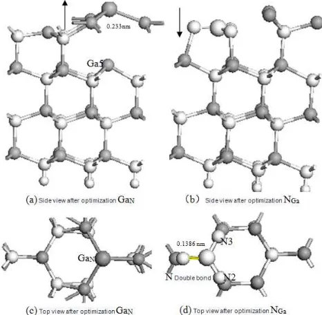
When a GaN defect forms at the surface, the substituting Ga atom bonds with the three nearest Ga atoms with a bond length of 0.233 nm. This is 4.5% shorter than the Ga–Ga bond (0.2440 nm) in α-Ga [18], the most stable structure of metallic Ga. The net charge of Ga2, Ga3, and Ga4 decreases from the original value (i.e., before GaN formation) of 0.71e to 0.22e.It shows that the bond between the substituting Ga atom and the adjacent Ga atoms exhibit considerable characteristics of a metallic bond. The Ga atoms that surround the substituting Ga atom (GaN) shift substantially outward from the surface (Fig.5). The GaN experiences a high repulsion from the Ga5and could not bond with it.
When an NGa defect forms at the surface, the surface structure changes remarkably. The substituting N-atom shifts significantly in the [0001] direction to a position only 0.0002 nm from N atoms in the immediate subsurface plane. The bonds between the surface Ga atoms and the N atoms adjacent to NGa are ruptured, creating an isolated Ga layer and an isolated N layer. The substituting N atom bonds with the adjacent N2 and N3 at bond lengths of approximately 0.1386 nm and connects to N4 with an N=N double bond (0.1382 nm, Fig. 5) that is significantly shorter than the original Ga-N bond (0.1986 nm). In addition, the net Mulliken charge of the N atoms adjacent to NGA increases from the original value of −0.980e to −0.620e; with such a decrease in the local electron density, the bonds between the substituting N atom and the adjacent N atoms become more covalent. In response to these changes in surface-atom positions, and bond lengths, as well as to the formation of N=N double bonds, the atoms surrounding the substituting N atom shift significantly toward the interior [Fig. 5(b)]. Because the total energy of a system containing an NGa defect is much higher than that containing a GaN defect, the NGa structure is highly unstable.
Fig 5. Side views and top views of optimized structure of the lattice in the
vicinity of GaN and NG defects; Ga; N; H
Fig 6. Side views and top views of optimized structures of the Ga
interstitial defects. Ga; N; H;
After a GaO interstitial defect is formed at the surface [Fig. 6(a)], the interstitial Ga shifts from its original interstitial position in the [0001] direction toward the surface and takes position in almost the same layer as other surface Ga atoms. The Ga1 moves to the vacuum layer above the surface and is located exactly above the N3 defect [Fig. 6(c)]. The original Ga1-N bond ruptures and Ga1 bonds with the newly adjacent Ga atoms by a Ga–Ga bond (0.2510 nm), which is slightly longer than the Ga–Ga bonds in α-Ga (0.2440 nm) [18]. The interstitial Ga [Fig. 6(c)] is exactly above the underlying N layer and bonds with the nearest N atoms with bond lengths ranging from 0.2012 to 0.2032 nm. The structure of the main lattice remains almost unchanged (0.1986 nm).
The stable structure of the lattice containing a GaT interstitial defect is similar to the structure of a lattice containing a GaO interstitial defect, but the Ga interstitial is farther from the surface Ga atoms. The Ga1 (originally at the surface) is exactly above the interstitial Ga [Figs. 6(b) and 6(d)]; they form a 0.2621-nm Ga–Ga bond, which is 7.4% longer than the Ga–Ga bond in α-Ga. These results indicate that the Ga interstitial atom shifts considerably, primarily because of the repulsion from adjacent Ga atoms.
that, compared with a Ga interstitial defect, an N interstitial defect is associated with a much higher energy, which is why it is unstable.
3.2. Energy of Point Defect Formation
We calculated the energies associated with the formation of various types of surface point defects in a manner similar to that done for the analyses of the native bulk point defects. In electrically neutral conditions, the formation energy
f
E (q = 0) of defects depends on the chemical potential
i
µ where
i
represents either a Ga or N atom. The formation energy of point defects is given byGa Ga N N
(defect) (perfect)
f T T
E =E −E +n µ +n µ (1)
where ET(defect) represents the total energy of the
defect-containing GaN unit cell, ET(perfect) represents the
total energy of the defect-free unit cell, µGa represents the
chemical potential of Ga atoms,
µ
N represents thechemical potential of N atoms,
n
Ga represents the numberof vacancy defects created by atom removal, and
n
Nrepresents the number of interstitial defects created by atom insertion. For example,
n
Ga = −1 andn
N = 0 representsthe existence of a Ga vacancy. The quantitiesET(defect) and ET(perfect) were calculated using the same parameters.
In GaN, the chemical potentials of Ga (µGa) and N (µN)
are influenced by the crystal-growth environment (i.e., Ga-rich or N-rich). Under thermodynamic equilibrium, the upper limit of max bulk
Ga Ga
µ =µ is satisfied in Ga-rich conditions and the other upper limit of max N2
N N
µ =µ is
satisfied in N-rich conditions. In this study, we approximated the chemical potentials by their corresponding single-point energies.
For a GaN crystal in a thermodynamic equilibrium, the following equation applies:
Ga
µ
+µ
N=E
T[
GaN
]
(2)where
E
T[
GaN
]
represents the total energy of a GaNmolecule in the GaN crystal, which we calculate to be −2333.23 eV. We find that the upper limit of
µ
Gacorresponds to the lower limit of
µ
N, so we can writemin bulk
N
E
T[GaN]
Gaµ
=
−
µ
(3)Similarly, in a GaN crystal, the upper limit of
µ
Ncorresponds to the lower limit of
µ
Ga, so we can write2
N min
Ga
[GaN]
Nµ
=
E
T−
µ
(4)The total energy of the GaN crystal in Eqs. (3) and (4) can be expressed as
2 N bulk Ga N [GaN] [GaN] T f
E =µ +µ + ∆H (5)
where ∆Hf[GaN] is the formation enthalpy of GaN,
which is negative when the GaN system is in stable conditions.
In addition, the stability of surface states is determined by the differences between the chemical potentials of Ga and N atoms and the respective chemical potential of the separate Ga crystal and N2 molecules, as described by the following equation:
bulk
i i i
µ µ µ
∆ = − (
i
=Ga, N) (6)According the above analyses, when a GaN crystal is grown slowly and stoichiometrically (Ga:N = 1:1) under equilibrium, the following equation applies:
Ga N Hf[GaN]
µ µ
∆ + ∆ = ∆ (7)
Following these methods, we calculate the formation enthalpy ∆Hf[GaN] of GaN to be −1.44 eV, which is
consistent with the results calculated by Grossner et al. who found −1.28 eV [19].
Table 3 summarizes the lattice parameters and the cohesive energy of α-Ga. Compared with the published values [20], the error is 2.1%, which implies that our calculation methods are reliable. We calculate the single-point energy of Ga in Ga single crystals to be −2061.38 eV. Similarly, we analyzed the structure and properties of N2. After structural optimization, the N≡≡N bond is determined to be 0.110 nm, and the bond energy is calculated to be −11.44 eV, both close to the experimentally measured values of 0.110 nm and −9.82 eV[20], respectively. We calculate the single-point energy of N to be −544.22 eV.
The formation energies of the eight types of point defects in Ga-rich as well N-rich conditions were calculated using Eq. (1) and the chemical-potential (Eqs. (3–5).) formulas are summarized in Tables 4 and 5 (ascending order from left to right).
The relative frequency different defects can be predicted based on the general rule that there is an inverse relationship between formation energy and probability of formation. Our calculations suggest that, in Ga-terminated surfaces (Table 4), GaO defects can form most easily, followed by GaN, and finally by VN and GaT defects. This trend may be understood based on the characteristics of Ga and N atoms. With a small ionic radius, Ga may easily diffuse into interstices to form interstitial defects. In contrast, N experiences a higher diffusion barrier and thus cannot easily migrate to interstices to form Frenkel defects. Therefore, NT and NGa defects are both associated with high formation energies, which makes it difficult for these interstitial defects to form.
defect from a surface terminated by Ga atoms is associated with the lowest formation energy (−0.76 eV), followed by NO, GaO, and VN defects. These results are consistent with the conclusion of Jürgen et al. that, in Ga-terminated polar surfaces, VGa defects are most stable. A comparison between Tables 4 and 5 suggest that, in both Ga-rich and
N-rich conditions, GaO (−1.173 eV), GaN (−0.73 eV) and VGa (−0.76 eV) defects can form more easily than VN defects. Compared with tetrahedral interstitial defects, octahedral interstitial defects are associated with lower formation energies and thus can form more easily.
Table 3. Lattice parameters and cohesive energy of α-Ga
α-Ga a(nm) b/a c/a Ecoh cohesion((((eV))))
Our Calculation 0.4822 0.908 1.629 -2.75
Experiment [22] 0.4511 1.001 1.695 -2.81
Table 4. Formation energies (eV) of point defects in GaN (0001) surface for Ga-rich conditions.
Types of defects GaO GaN VN GaT VGa NO NT NGa
Ga-rich -1.173 -0.73 -0.49 0.068 0.68 1.647 3.95 5.713
Table 5. Formation energies (eV) of point defects in GaN (0001) surface for N-rich conditions.
Types of defects VGa NO GaO VN GaT GaN NT NGa
N-rich -0.76 0.207 0.269 0.95 1.508 2.148 2.51 2.833
4. Conclusions
This study shows that VGa and VN defects only slightly modify the positions of adjacent atoms and induce limited surface relaxation. In comparison, GaN and NGa defects oblige adjacent atoms to substantially shift outward from the surface, with the NGa-induced shift being particularly significant. Moreover, N=N double bonds form at the surface. The total energy of a system containing NGa defects is much higher than for a system containing GaN defects, so the NGa-defect structure is highly unstable.
The stable structures of GaT and GaO defects are similar, but the Ga atom in the tetrahedral interstice is farther from adjacent atoms than is the case for the octahedral interstice. Compared with Ga interstitial defects, N interstitial defects, particularly NO, induce larger surface distortions. Structural optimization and calculations reveal that the N–Ga bonds in the second nearest layer are ruptured, which greatly influences the deep-lattice structure. The total energy of systems containing N interstitial defects is much higher than for systems containing Ga interstitial defects, so the former are less stable than the latter.
We also calculated the formation energies of various defects. Our results predict that, in both Ga-rich and N-rich conditions, GaO (formation energy of −1.173 eV), GaN (−0.73 eV), and VGa (−0.76 eV) defects can more easily form than VN (−0.95eV) defects, which suggests that Ga-related defects are generally easier to form than N-related defects. In addition, octahedral interstitial defects are associated with lower formation energies than tetrahedral interstitial defects and thus can form more easily. NT and NGa defects have the highest formation energies, suggesting that N-related defects are the most difficult to form.
Acknowledgment
This research work was supported by the
NationalNatural Science Foundation of China (Grant Nos. 51172150 and 50942025).
References
[1] S.C.Binari, W.Kruppa, H.B.Dietrich, G.Kelner, A. E.Wickenden, J.A.Freitas, Solid- State Electron. 1 (1997) 1549.
[2] R.Gaska,Q.Chen, J.Yang, A.Osinsky, M. Asifkhan, M.S.Shur, IEEE Electron. Dev. Lett. 18 (1997) 492.
[3] G. J.Sullivan, M.Y.Chen, J. A.Higgins, J.W.Yang, Q.Chen, . P. L.Pierson, B. T.McDermott, IEEE Electron. Dev. Lett. 19 (1998.) 198.
[4] B.Heying, R.A.verbeck, L.F.Chen, E.Haus, H.Riechert, J.S.Speck, J. Appl. Phys. 88 (2000) 1855.
[5] L. X.Zheng, M.H.Xie, S.M.Seutter, S.H.Cheung, S.Y.Tong, Phys. Rev. Lett. 85 (2000) 2352.
[6] C.Adelmann, J.Brault, G.Mula, B.Daudin, L.Lymperakis, J.Neugebauer, Phys. Rev. B. 67 (2003) 165419.
[7] G.Koblmüller, R.Averbeck, H. Riechert, P.Pongratz, Phys. Rev. B. 69 (2004) 035325.
[8] N. M. Harrison, Comput.Phys. Commun. 137 (2001) 59-73.
[9] Chun Yang, Yang Chong, P.Huang, X.Q.Liang, Surf. Rev. Lett. 6 (2011) 315-321.
[10] E.William, J.Packard, D.Dow, J. Mater. Res. 3 (1997) 646-650.
[12] K.Saarinen, T.Suski, I.Grzegory, D.C.Look, Phys. Rev. B. 64 (2001) 233201.
[13] K.H.Chow, G.D.Watkins, A. Usui, M.Mizuta, Phys. Rev. Lett. 85 (2000) 2761-2764.
[14] K.Burke, J.P.Perdew, Y.Wang, Electronic Density Functional Theory, Recent Progress and New Directions,Plenum Press Inc., New York, 1998.
[15] J. P.Perdew, K.Burke, M.Ernzerhof, 1996. Phys. Rev. Lett. 77, 3865-3868.
[16] B.Hammer, L. B.Hansen, J.K.Norskov, Phys. Rev. B. 59 (1999) 7413-7421
[17] T. H.Fischer, J.Almlof, J. Phys. Chem. 96 (1992) 9768-9774.
[18] R.W.G.Wyckoff, Crtstal Structures. Wiley Inc., New York, 1962.
[19] U.Grossner, J.Furthmüller, F.Bechsted, Phys. Rev. B. 59 (1999) 15166-15180