Nano-mechanical Behaviour and Mmicrostructural Evolution of Cu/Si
Thin Films at Different Annealing Temperatures
Woei-Shyan Lee
1,*, Tao-Hsing Chen
2, *, Chi-Feng Lin
3and Yu-Liang Chuang
11Department of Mechanical Engineering, National Cheng Kung University, Tainan 701, Taiwan
2Department of Mechanical Engineering, National Kaohsiung University of Applied Sciences, Kaohsiung 807, Taiwan
3National Center for High-Performance Computing, National Applied Research Laboratories, Hsin-Shi Dist., Tainan City744,
Taiwan
Received 05 May 2012; received in revised form 30 May 2012; accepted 02 July 2012
Abstract
This study investigates the nano-mechanical properties of as-deposited Cu/Si thin films indented to a depth of 2000 nm using a nanoindentation technique. Cu films with a thickness of 1800 nm are deposited on (100) silicon substrates and the indented specimens are then annealed at temperatures of 160℃ and 210℃, respectively, using
rapid thermal annealing (RTA) technique. The results show that the hardness and Young’s modulus of the Cu/Si thin films have maximum values of 0.82 GPa and 95 GPa, respectively. The TEM observations show that the specimens annealed at a temperature of 160℃, the amorphous nature of the microstructure within the indented zone is
maintained. However, annealed at a higher temperature of 210℃, the indentation affected zone consists of Copper
silicide (η-Cu3Si) precipitates are observed in the annealed specimens. Overall, the results presented in this study
confirm that the annealing temperature has a significant effect on the formation of η-Cu3Si in nanoindented Cu/Si
thin-film systems.
Keywords: Nanoindentation, Silicon, Microstructural evolution, Annealing temperature
1.
Introduction
Silicon is one of the most commonly used substrate materials in the microelectronics and optoelectronics industry due to its excellent semiconducting properties. Face-centered cubic (fcc) films deposited on silicon substrates are widely used as metallic contacts at the micro- and macro-scales [1-3]. The mechanical properties of thin-film materials are typically very different from those of the corresponding bulk materials [4, 5]. Therefore, in optimising the thin-film structures used in MEMS and integrated circuit (IC) applications, it is necessary to study the mechanical properties and microstructure of the thin-film system at an appropriate (i.e. nanometer) scale.
Nanoindentation technology provides a convenient method to analyze the mechanical properties of both bulk materials and thin films [6, 7]. Previous articles have shown that the indentation process results in a pressure-induced phase transformation of the material directly beneath the indenter, which has a direct effect on the characteristics of the corresponding load-displacement curve [7, 8]. The loading curve obtained during the nanoindentation process often exhibits a discontinuity referred to as a “pop-in” event [9], while the unloading curve sometimes contains a discontinuity referred to as a
“pop-out” event [10]. In general, both events are indicative of a change in the phase transformation mechanism under the corresponding indentation load. Furthermore, it has been shown that the indented microstructure of an as-deposited specimen can be modified via the application of a suitable annealing temperature [8, 11].
Amongst all the face-centered cubic (fcc) materials, copper (Cu) tends to be one of the most commonly used for the coating of silicon substrates in the fabrication of modern electronic devices dues to its high chemical stability, low resistivity, good patterning ability, good reliability, ready availability, and low cost [12, 13]. Various physical and chemical methods have been proposed for the fabrication of Cu/Si systems with coherent layers [14-17].
It is known that the bonding strength of the Cu/Si system is enhanced via the precipitation of copper silicide particles and via a solid state reaction when the interface between the thin Cu film and the Si substrate is heated to a sufficient temperature. Accordingly, this study investigates the nano-mechanical properties of as-deposited Cu/Si samples indented to a depth of 2000 nm and then anneals the indented samples at temperatures of either 160℃ or 210℃, respectively.
Thereafter, the microstructures of the as-deposited and annealed samples are examined via transmission electron microscopy (TEM) in order to examine the effects of the annealing temperature on the microstructural evolution of the indented specimens and the degree of copper silicide formation.
2.
Experimental procedure
The Cu films with a thickness of 1800 nm were deposited on Si (100) wafers using an evaporation deposition technique. During the deposition process, the substrate was maintained at a temperature of 150℃ to improve the homogeneity of the
evaporated film and the chamber pressure was maintained at a constant 10-5 ~ 10-7 Torr. The thickness of the Cu film was
monitored continuously during the deposition process using a quartz-crystal microbalance, and was confirmed following fabrication using an X-ray reflectometry technique.
The nanoindentation tests were performed using an MTS Nanoindenter XP system fitted with a Berkovich diamond pyramid tip. The loading-unloading procedure involved the following steps: (1) loading to the maximum indentation depth (2000nm) at a constant rate of 0.2 mN/s, (2) holding at this depth for 10 s, and (3) smoothly unloading over a period of 30 s. The hardness and Young’s modulus of the as-deposited Cu/Si thin film were then calculated from the loading-unloading curve using the Oliver and Pharr method [18].
Following the nanoindentation tests, the specimens were annealed at a temperature of either 160℃ or 210℃ for 2 min in
a rapid thermal annealing (RTA) system. During the annealing process, purified nitrogen gas (99.999%) was passed through the furnace at a flow rate of 3L / min. Thin foil specimens of both the as-deposited samples and the annealed samples were prepared using an FEI Nova 200 focused ion beam (FIB) milling system with a Ga+ ion beam and an operating voltage of 30
keV.
3.
Results and discussion
3.1. Nano-mechanical behaviour of Cu/Si thin film
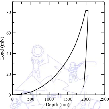
The loading-unloading curve for the as-deposited Cu/Si thin film when indented to a depth of 2000 nm is shown in Fig. 1. It can be seen that both the loading and the unloading regions of the curve are smooth and continuous, which suggests that no debonding or cracking occurs during the indentation process. The unloading portion of the load-displacement curve in Fig. 1 has a smooth, step gradient and a slight elbow can be seen in the final part of the unloading curve. Moreover, the virtually vertical slope of the unloading curve indicates that the plastic deformation of the Cu/Si thin film during the loading process is followed by a very weak elastic return in the unloading step. It is noted that the presence of slight elbow feature in the final portion of the unloading curve suggests that the silicon substrate transforms from a diamond cubic structure to an amorphous structure in the indentation affected zone.
0 500 1000 1500 2000 2500
Depth (nm) 0 20 40 60 80 Lo ad ( m N)
Fig. 1 Typical load-displacement curve obtained in nanoindentation test performed to depth of 2000 nm
0 500 1000 1500 2000 2500
Depth(nm) 0 1 2 3 4 5 Ha rdne ss ( G Pa ) Fig. 2 Variation of microhardness with indentation depth
It presents the variation of the Young’s modulus of the Cu/Si system against the nanoindentation depth in Fig. 3. It is observed that the Young’s modulus reduces significantly as the indenter first penetrates the Cu/Si thin film. However, the modulus value then increases rapidly with an increasing indentation depth, and reaches a final value of approximately 95 GPa at the maximum indentation depth of 2000 nm.
Moreover, the presence of the Cu layer on the upper surface of the Si substrate reduces the final value of the Young’s modulus compared to that of an uncoated Si (100) substrate (i.e. 169.0 GPa [21]). However, the Young’s modulus of the Cu/Si system is still significantly higher than that of a pure Cu thin film (i.e. 99 ~ 123 GPa [22]).
0 500 1000 1500 2000 2500
Depth(nm)
0 1 2 3 4 5
Ha
rdne
ss
(
G
Pa
)
Fig. 3 Variation of Young’s modulus with indentation depth
3.2. Indented microstructure of as –deposited and annealed Cu/Si thin films
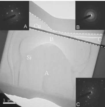
Fig. 2 presents a cross-sectional TEM image of an as-deposited Cu/Si specimen indented to 1800μm. The insets in the upper-right and upper-left corners of Fig. 2 show the TEM diffraction patterns of the regions of the specimen indicated by the white squares A and B, respectively. The results show that in the as-deposited condition, the indentation affected zone of the Cu/Si system has an amorphous phrase, while the silicon substrate has a diamond cubic structure.
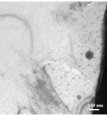
It shows the TEM micrograph of the indented microstructure of Cu/Si specimen annealed at a temperature of 160℃ for
2 min in Fig. 5. It can be seen from the following annealing process, the microstructure of the indentation affected zone is still composed entirely of amorphous phase (see also the high-resolution TEM micrograph presented in Fig. 6). Fig. 7 presents a high-magnification TEM micrograph of the indentation affected zone and shows that the annealing temperature of 160℃
prompts the uniform precipitation of copper silicide (η-Cu3Si) particles in the upper region of the indented zone.
Fig. 5 Bright field TEM micrograph of indented specimen annealed at 160℃
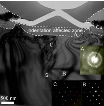
Fig. 8 and 9 present TEM micrographs of the indentation affected zone in a specimen annealed at a higher temperature of 210℃. It is observed that the indentation affected zone has a mixed structure comprising amorphous phase, copper silicide
η-Cu3Si phase and nanocrystalline phase.
Fig. 10 presents a high-magnification TEM micrograph of the indentation affected zone and shows that the annealing temperature of 210℃ prompts the uniform precipitation of copper silicide (η-Cu3Si) particles in the upper region of the
indented zone. Fig. 11 presents a high-resolution TEM micrograph of the η-Cu3Si precipitates in Fig. 10. It can be seen that the
indented matrix microstructure surrounding the η-Cu3Si precipitate has an amorphous phase, while the precipitate itself has a
crystalline structure (as confirmed by the diffraction spots in the diffraction pattern shown in the inset in Fig. 9).
The lattice spacing of the η-Cu3Si precipitates is found to be 2.01±0.02Å, which is in good agreement with the results
reported by Bouayadi et al. [19], and is close to the value of the {110} plane spacing given in the literature (i.e. 2.02Å [24]). Comparing Figs. 7 and 10, it is can be clearly observed that the copper silicide η-Cu3Si phase increases with an increasing
annealing temperature.
Fig. 8 Bright field TEM micrograph of indented specimen annealed at 210℃
Fig. 10 The copper silicide η-Cu3Si precipitates within indentation affected zone in specimen annealed at 210℃
η-Cu3Si
Fig. 11 High-resolution TEM micrograph of copper silicide precipitates
4.
Conclusions
This study investigates the nano-mechanical properties of as-deposited Cu/Si thin films indented to a maximum depth of 2000 nm. The indented specimens were then annealed at a temperature of either 160℃ or 210℃, and the microstructures of the
as-deposited and annealed samples were examined using transmission electron microscopy (TEM). The results have shown that the loading and unloading regions of the load-displacement curves obtained in the nanoindentation tests have a smooth and continuous profile. Moreover, it has shown that the present Cu/Si thin films have a maximum hardness and Young’s modulus of 0.82 GPa and 95 GPa, respectively.
The TEM observations have shown that for both the as-deposited specimens and the specimens annealed at a temperature of 160℃, the indentation process prompts a change in the microstructure within the indentation affected zone
from a diamond cubic structure to an amorphous phase. However, at a higher annealing temperature of 210℃, the
microstructure of the indentation affected zone contains a mixture of amorphous phase and nanocrystalline phase. The TEM observations have also shown that the copper silicide (η-Cu3Si) phases could be observed at the higher annealed temperature
Acknowledgements
The authors gratefully acknowledge the financial support provided to this study by the National Science Council (NSC) of Taiwan under contract no. NSC 97-2221-E-006-047.
References
[1] Y. Cao, C. Kim, S. R. Forrest and W. O. Soboyejo, “Patterning of active organic materials by direct transfer for organic electronic devices,” Journal of applied physics, vol. 98, pp. 033713, May 2005.
[2] S. Majumder, N. E. McGruer, G. G. Adams, P. M. Zavracky, R. H. Morrison and J. Krinm, “Study of contacts in an electrostatically actuated microswitch,” Sensors and Actuators A: Physical, vol. 93 pp. 19-26, July 2001.
[3] J. Plummer, M. Deal and P. Griffin, Silicon VLSI Technology: Fundamental, Practice and Modeling, New Jersey: Prentice Hall, 2000.
[4] R. Saha and W. D. Nix, “Effects of the substrate on the determination of thin film mechanical properties by nanoindentation,” Acta Materialia, vol. 50, pp. 23-28, 2002.
[5] J. Lou, P. Shrotriya, T. Buchheit, D. Yang, W. O. Soboyejo, “Nanoindentation study of plasticity length scale effects in LIGA Ni microelectromechanical systems structures,” Journal of Materials Research, vol. 18, pp 719-728, 2003. [6] A. C. Fischer-Cripps, Nanoindentation, Berlin: Springer-Verlag, 2002.
[7] W. S. Lee and F. J. Fong, “Eutectic and Amorphous Phase Formation at Au/Cr/Si Thin Film Interface by Nanoindentation and Annealing,” Materials Transactions, vol. 48, pp. 2650-2658, 2007.
[8] W. S. Lee and T. Y. Liu, “The effect of annealing temperature on the microstructure of nanoindented Au/Cr/Si thin films,” Nanotechnology, vol. 18, pp. 335701, 2007.
[9] J. E. Bradby, J. S. Williams, J. Wong-Leung, M. V. Swain and P. Munroe, “Mechanical deformation in silicon by micro-indentation,” Journal of Materials Research, vol. 16, pp. 1500-1507, 2001.
[10]V. Domnich and Y. Gogotsi, “Phase transformations in silicon under contact loading,”Reviews on Advanced Materials Science, vol. 3, pp. 1-36, 2002.
[11]W. S. Lee and F. J. Fong, “Microstructural study of annealed gold–silicon thin films under nanoindentation,” Materials Science and Engineering A, vol. 475 pp. 319-327, 2008.
[12]A. Cros, M. O. Aboelfotoh and K. N. Tu, “Formation, oxidation, electronic, and electrical properties of copper silicides,” Journal of applied physics, vol. 67, pp. 3328-3336, 1990.
[13]R. J. Gutmann, T. P. Chow, A. E. Kaloyeros, W. A. Lanford and S. P. Muraka, “Thermal stability of on-chip copper interconnect structures,” Thin Solid Films, vol. 262, pp. 177-186, 1995.
[14]M. Y. Park, J. H. Son and S. W. Rhee, “Chemical Vapor Deposition of Copper Thin Films with
(hexafluoroacetylacetonate) Cu (allyltrimethylsilane),”Electrochemical and solid-state letters, vol. 1, pp. 32-33, 1998. [15]D. K. Kwak, H. B. Lee, J. W. Han and S. W. Kang, “Metalorganic chemical vapor deposition of copper on ruthenium thin
film,” Electrochemical and solid-state letter, vol. 9, pp. C171-C173, 2006.
[16]O. Azzaroni, M. Fonticelli, P. L. Schilardi, G. Benitez, I. Caretti, J. M. Albella, R. Gago, L. Vazquez and R. C. Salvarezza, “Silver electrodeposition on nanostructured gold: from nanodots to nanoripples,” Nanotechnology, vol. 15, pp.
S197-S200, 2004.
[17]M. F. sharin, A. Razak and Z. Zainal, “Electrophoretic deposition and characterization of copper selenide thin films,” The Malaysian Journal of Analytical Science, vol. 11, pp. 324-330, 2007.
[18]W. C. Oliver and G. M. Pharr, “Improved technique for determining hardness and elastic modulus using load and displacement sensing indentation experiments,” Journal of Materials Research, vol. 7, pp. 1564-1580, 1992.
[19]R. E. Bouayadi, G. Regula, B. Pichaud, M. Lancin, C. Dubois and E. Ntsoenzok, “Gettering of diffused Au and of Cu and Ni contamination in silicon by cavities induced by high energy He implantation,” Physica Status Solidi B, vol. 222, pp. 319-326, 2000.
[20]D. Christopher, R. Smith and A. Richter, “Atomistic modelling of nanoindentation in iron and silver,” Nanotechnology, vol. 12, pp. 372-383, 2001.
[22]S. H. Hong, K. S. Kim, Y. M. Kim, J. H. Hahn, C. S. Lee, and J. H. Park, “Characterization of elastic moduli of Cu thin films using nanoindentation technique”, Composites Science and Technology, vol. 65, pp. 1401-1408, 2005.