Learning Acyclic Probabilistic Circuits Using Test Paths
Dana Angluin [email protected]
James Aspnes [email protected]
Department of Computer Science Yale University
New Haven, CT 06520
Jiang Chen [email protected]
Yahoo! Inc. 701 First Avenue Sunnyvale, CA 94086
David Eisenstat [email protected]
55 Autumn St.
New Haven, CT 06511
Lev Reyzin [email protected]
Department of Computer Science Yale University
New Haven, CT 06520
Editor: Rocco Servedio
Abstract
We define a model of learning probabilistic acyclic circuits using value injection queries, in which fixed values are assigned to an arbitrary subset of the wires and the value on the single output wire is observed. We adapt the approach of using test paths from the Circuit Builder algorithm (Angluin et al., 2009) to show that there is a polynomial time algorithm that uses value injection queries to learn acyclic Boolean probabilistic circuits of constant fan-in and log depth. We establish upper and lower bounds on the attenuation factor for general and transitively reduced Boolean probabilistic circuits of test paths versus general experiments. We give computational evidence that a polynomial time learning algorithm using general value injection experiments may not do much better than one using test paths. For probabilistic circuits with alphabets of size three or greater, we show that the test path lemmas (Angluin et al., 2009, 2008b) fail utterly. To overcome this obstacle, we introduce function injection queries, in which the values on a wire may be mapped to other values rather than just to themselves or constants, and prove a generalized test path lemma for this case.
Keywords: nonadaptive learning algorithms, probabilistic circuits, causal Bayesian networks, value injection queries, test paths
1. Introduction
gene will be active (Friedman et al., 2000). In the independent cascade model of social networks, the state of each agent is active or inactive and for each pair(u,v)of agents, there is a probability that the activation of u will cause v to become active. Kempe, Kleinberg, and Tardos (2003, 2005) study the problem of maximizing influence in this and related models of social networks. In a Bayesian network there is an acyclic directed graph and a joint probability distribution over the node values such that the joint distribution is the product of each of the marginal distributions for each node given the values of the parents (in-neighbors) of the node.
A fundamental question is how much we can infer about the properties and structure of such networks from observing and experimenting with their behaviors. Prior research gives evidence from cryptography that there may be no polynomial time algorithm to learn Boolean functions represented by acyclic circuits of constant fan-in and depth O(log n) when we can set only the inputs of the circuit and observe only the output (Angluin and Kharitonov, 1995). In this paper we consider a different setting, value injection queries, in which we can fix the values on any subset of wires in the target circuit, but still only observe the output of the circuit.
The concept of value injection queries was inspired by models of gene suppression and gene overexpression in the study of gene interaction networks (Akutsu et al., 2003; Ideker et al., 2000) and was introduced by Angluin et al. (2009). In a causal Bayesian network there is an additional action do(X=x) that forces a node X to take on a value x (Pearl, 2000). A value injection query may also be viewed as a set of such actions, one for each wire fixed to a value.
Angluin et al. (2009) investigate the learnability of deterministic circuits using value injection queries and behavioral equivalence queries. Polynomial time learning algorithms using just value injection queries are given for two classes of acyclic circuits. Circuit Builder uses value injection queries to learn acyclic deterministic circuits with constant-size alphabets, constant fan-in and depth
O(log n) up to behavioral equivalence in polynomial time. Another algorithm is given that learns constant-depth acyclic Boolean circuits with NOT gates and unbounded fan-in AND, OR, NAND and NOR gates up to behavioral equivalence in polynomial time using value injection queries. Neg-ative results include an exponential lower bound on the number of value injection queries to learn acyclic Boolean circuits of unbounded depth and unbounded fan-in, and the NP-hardness of learning acyclic Boolean circuits of unbounded depth and constant fan-in using value injection queries.
In extending these results to analog circuits, Angluin et al. (2008b) consider circuits with polynomial-size alphabets. They give evidence of the computational hardness of learning acyclic circuits over a polynomial-size alphabet even if the depth is restricted to O(log n), motivating struc-tural restrictions on the graphs of the circuits to achieve polynomial time learnability. They give the Distinguishing Paths Algorithm, which uses value injection queries and learns acyclic deterministic circuits that are transitively reduced and have polynomial-size alphabets, constant fan-in and un-bounded depth up to behavioral equivalence in polynomial time. They also give a generalization to circuits with a constant bound on shortcut width.
In this paper we seek to extend some of these positive learnability results to the case of acyclic probabilistic circuits. The key technique in the previous work has been the idea of a test path for an arbitrary wire w in the circuit. Informally speaking, a test path is a directed path of wires from
w to the output wire in which each wire is an input of the next wire on the path, and the other
wire w. The primary focus of this paper is to understand the properties of test paths in probabilistic circuits, and the extent to which they can be used to give polynomial time algorithms for learning probabilistic acyclic circuits.
In Section 2 we formally define our model of acyclic probabilistic circuits, value injection queries and distribution injection queries, behavioral equivalence, and the learning problem that we consider. In Section 3 we establish some basic results about probabilistic circuits and value and distribution injection experiments. In Section 4 we review the test path lemma used in previous work to establish the ability of a learner to infer circuit behavior from a small subset of experiments and show that it fails utterly in probabilistic circuits with alphabet size greater than two. However, for Boolean probabilistic circuits, we show that the test path lemma holds with an attenuation factor that depends on the structure of the circuit. (Lemma 10 treats general acyclic circuits and Corol-lary 11 specializes the bound to transitively reduced circuits.) In Section 5 we apply the test path lemma in the Boolean case to adapt the Circuit Builder algorithm (Angluin et al., 2009) to find using value injection queries, with high probability, in time polynomial in n and 1/ε, a circuit that isε-behaviorally equivalent to a target acyclic Boolean probabilistic circuit of size n with constant fan-in and depth bounded by a constant times log n. In Section 6, we consider lower bounds on the attenuation of paths; Theorem 16 shows that our bound is tight for transitively reduced circuits and Theorem 18 gives a lower bound for the case of general acyclic circuits. In Section 7 we give evidence that polynomial time algorithms using general value injection experiments may not do significantly better than algorithms that use test paths. In Section 8 we introduce a stronger kind of query, a function injection query, and show that test paths with function injections overcome the limitations of test paths for circuits with alphabets of size greater than two.
2. Model
We extend the circuit learning model (Angluin et al., 2008b, 2009) to probabilistic gates. An unusual feature of this model is that circuits do not have distinguished inputs—since the learning algorithm seeks to predict the output behavior of value injection experiments that override the values on an arbitrary subset of wires, each wire is a potential input.
2.1 Probabilistic Circuits
A probabilistic circuit C of size n≥1 has n wires, of which one is the distinguished output wire. We call the set of C’s wires W , and these wires take values in a finite alphabetΣwith|Σ| ≥2. If
Σ={0,1}, then C is Boolean. The value on a wire is ordinarily determined by the output of an associated probabilistic gate, whose distribution is a function of the values on other wires.
Formally, a value distribution D is a probability distribution overΣ, that is, a map fromΣto the real interval[0,1]such that∑σ∈ΣD(σ) =1. The probability ofσis D(σ). The support of D is the set of values σ∈Σsuch that D(σ)>0. When the support of D is a singleton{σ}, we say
D is deterministic. For a nonempty set of values S⊆Σ, the uniform distribution U(S) is the distribution such that U(S)(σ) = [σ∈S]/|S|, that is, has value 0 onσ6∈S and 1/|S|forσ∈S.
A probabilistic gate g of fan-in k pairs a k-ary probabilistic gate function f with a k-tuple (w1, . . . ,wk)∈Wkof input wires. The gate g is deterministic if its gate function f is deterministic. When k=0, the gate g has no inputs, and we can regard it as specifying a value distribution, or, when C is Boolean, a biased coin flip.
A probabilistic circuit C maps wires to probabilistic gates. C is deterministic if all of its gates are deterministic. The fan-in of C is the maximum fan-in over C’s gates. The circuit graph of C has a node for each wire in W and a directed edge(u,w)if u is one of the input wires of the gate associated with w. It is important to distinguish between wires in the circuit and edges in the circuit graph. For example, if wire u is an input of wires v and w, then there will be two directed edges, (u,v)and(u,w), in the circuit graph.
Wire w is reachable from wire u if there is a directed path from u to w in the circuit graph. A wire is relevant if the output wire is reachable from it. The depth of a wire w is the number of edges in the longest simple path from w to the output wire in the circuit graph. The depth of the circuit is the maximum depth of any relevant wire. The circuit is acyclic if the circuit graph contains no directed cycles. The circuit is transitively reduced if its circuit graph is transitively reduced, that is, if it contains no edge(u,w)such that there is a directed path of length at least two from u to w. In this paper we assume all circuits are acyclic.
2.2 Experiments
In an experiment some wires are constrained to be particular values or value distributions and the other wires are left free to take on values according to their gate functions and the values of their input wires. The behavior of a circuit consists of its responses to all possible experiments. For probabilistic circuits we consider both value injection experiments and distribution injection exper-iments.
A distribution injection experiment e is a function with domain W that maps each wire w to a special symbol∗or to a value distribution. A value injection experiment e is a distribution injection experiment for which every value distribution assigned is deterministic—that is, always generates the same symbol. To simplify notation, we think of a value injection experiment as a mapping from W to (Σ∪ {∗}). If e is either kind of experiment, we say that e leaves w free if
e(w) =∗; otherwise we say that e constrains w to e(w). If e(w)is a single symbol, then we say e fixes w to e(w).
We define a partial ordering≤on the set containing∗and all value distributions D as follows:
D≤ ∗for every value distribution D, and for two value distributions, D1≤D2if the support of D1 is a subset of the support of D2. This ordering is extended to experiments on the same set of wires
W as follows: e1≤e2 if for every w∈W , e1(w)≤e2(w). The intuitive meaning of e1≤e2is that
e1is at least as constraining as e2for every wire.
If e is any experiment, w is a wire, and a is∗ or an element ofΣor a value distribution, then the experiment e|w=ais defined to be the experiment e′such that e′(w) =a and e′(u) =e(u)for all
u∈W such that u6=w. If e is any experiment then a free path in e is a path in the circuit graph
containing only wires w that are free in e.
2.3 Behavior
is constrained then w is randomly and independently assigned a value inΣdrawn according to the value distribution e(w); in the case of a value injection experiment, this just assigns a fixed element ofΣto w. If wire w is free and has probabilistic gate function f , and its inputs u1, . . . ,uk have been assigned the valuesσ1, . . . ,σk, then w is randomly and independently assigned a value fromΣ ac-cording to the value distribution determined by the gate function on these inputs, that is, acac-cording to the value distribution f(σ1, . . . ,σk).
Constrained gates and gates of fan-in zero give the base cases for the above recursive definition, which assigns an element ofΣto every wire because the circuit is acyclic. Let C(e,w) denote the (marginal) value distribution of the assignments of values to w for the above process. The output distribution of the circuit, denoted C(e), is the distribution C(e,z), where z is the output wire of the circuit. The behavior of a circuit C is the function that maps value injection experiments e to output distributions C(e).
We note that even when the circuit is Boolean and the only non-deterministic gates are uniform coin flips, the problem of exactly computing C(e)is #P-hard because we can arrange for C(e)to be the fraction of assignments satisfying a given Boolean formula.
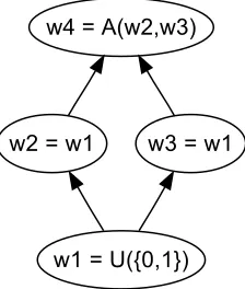
2.4 Example: C1
We give an example of a simple Boolean probabilistic circuit, which we also refer to later. The 2-input averaging gate function A(b1,b2) outputs 1 with probability (b1+b2)/2. Thus, if both inputs are 0, the output is deterministically 0, if both inputs are 1, the output is deterministically 1, and if its inputs disagree, the output is an unbiased coin flip, U({0,1}). Another characterization of the averaging gate function A is that it randomly and equiprobably selects one of its inputs and copies it to the output.
We define a circuit C1 of 4 wires as follows: w4=A(w2,w3), w3 =w1, w2=w1, and w1=
U({0,1}). The output wire is w4. C1is depicted in Figure 1.
w1 = U({0,1}) w2 = w1 w3 = w1
w4 = A(w2,w3)
Figure 1: The circuit C1; w4is the output wire.
0. It is easy to see that this is one of two possible outcomes for experiment e; either all wires are assigned 0 or all wires are assigned 1, and these each occur with probability 1/2. The output distribution C1(e)is just an unbiased coin flip.
Now consider experiment e′=e|w2=1 that fixes w2 to 1 and leaves the other wires free. Once
again, the value of w1 is determined by a coin flip—say it is assigned 0. Since w2 is fixed to 1, that is its assignment. Wire w3is free, and is therefore assigned the value of w1, that is 0. Now the inputs of w4 have been assigned values, so we consider A(1,0), which randomly and equiprobably selects 0 or 1. If, instead, the coin flip for w1had returned 1, all wires would be assigned 1. There are three possible assignments to(w1,w2,w3,w4)for experiment e′:(1,1,1,1)with probability 1/2, (0,1,0,0)with probability 1/4 and(0,1,0,1)with probability 1/4. The output distribution C1(e′) is a biased coin flip that is 1 with probability 3/4.
2.5 Behavioral Equivalence
Two circuits C and C′are behaviorally equivalent if they have the same set of wires, the same out-put wire and the same behavior, that is, for every value injection experiment e, C(e) =C′(e). We also need a concept of approximate equivalence. The (statistical) distance between value distributions
D and D′is d(D,D′) = (1/2)∑σ|D(σ)−D′(σ)|, which takes values in[0,1]. Note that when D and
D′are deterministic, d(D,D′)is 0 if D=D′and 1 otherwise. Forε≥0, C isε-behaviorally equiv-alent to C′ if they contain the same wires and the same output wire, and for every value injection experiment e, d(C(e),C′(e))≤ε, where d is the statistical distance between value distributions.
In Lemma 2 we show that the behavioral equivalence of C and C′ implies C(e) =C′(e)for all distribution injection experiments as well. However, behavioral equivalence is not sufficient to guar-antee that two circuits have the same topology; even when all the gates are Boolean, deterministic and relevant, the circuit graph of the target circuit may not be uniquely determined by its behavior (Angluin et al., 2009).
2.6 Queries
The learning algorithm gets information about the target circuit by specifying a value injection ex-periment e and observing the element ofΣassigned to the output wire. Such an action is termed a value injection query, abbreviated VIQ. A value injection query does not return complete informa-tion about the value distribuinforma-tion C(e), but instead returns an element ofΣselected according to the distribution C(e). Thus, in order to approximate the distribution C(e), the learner must repeatedly make value injection queries with experiment e. In this case, the goal of learning is approximate behavioral equivalence.
2.7 The Learning Problem
The learning problem is ε-approximate learning: by making value injection queries to a target circuit C drawn from a known class of probabilistic circuits, the goal is to find a circuit C′ that is
ε-behaviorally equivalent to C. The inputs to the learning algorithm are the names of the wires in C, the name of the output wire and positive numbersεandδ, where the learning algorithm is required to succeed with probability at least(1−δ).
equivalent to C, then we can compute the behavior of C on any value-injection experiment e with high probability by sampling the behavior of C′(e). The negative results concerning learning deter-ministic circuits using value injection queries shown by Angluin et al. (2009) carry over to learning probabilistic circuits. In particular, for ε=1/3 and δ=1/2, with no bound on fan-in or depth, the worst-case expected number of value injection queries necessary to learn acyclic probabilistic Boolean circuits is exponential, while with constant fan-in and no bound on depth, no polynomial time algorithm can learn acyclic probabilistic Boolean circuits if NP is not equal to BPP.
3. Preliminary Results
In this section we establish some basic results about probabilistic circuits, value injection experi-ments and distribution injection experiexperi-ments. The reader may choose to skip this section and return to it as needed for proofs in subsequent sections.
We first note that if C is a probabilistic circuit, e is a distribution injection experiment and either
e(w)is a value distribution or e deterministically fixes all the input wires of w, then there is a value distribution D such that the value of w in C(e)is determined by a random choice according to D, independent of the values chosen for any other wires. We make systematic use of this observation to reduce the number of experiments under consideration.
We start by considering two circuits C1 and C2 over the same wires, and distribution injection experiments e1 and e2 that agree on the distribution assigned to a wire w and that show a certain distance between C1(e1)and C2(e2). The following lemma says that we may modify e1 and e2to fix w to a particular valueσ∈Σwhile preserving (or increasing) the distance they show.
Lemma 1 Let C1and C2be probabilistic circuits on wires W with the same output wire, let w∈W
be a wire, let D be a value distribution, and let e1and e2be distribution injection experiments such
that e1(w) =e2(w) =D. Then there exists a valueσ∈support(D)such that
d(C1(e1|w=σ),C2(e2|w=σ))≥d(C1(e1),C2(e2)).
Proof We have
d(C1(e1),C2(e2)) =1 2τ∈Σ
∑
C1(e1)(τ)−C2(e2)(τ)
=1 2τ∈Σ
∑
ρ∈Σ
∑
C1(e1|w=ρ)(τ)D(ρ)−ρ∈Σ∑
C2(e2|w=ρ)(τ)D(ρ) ≤12ρ∈Σ
∑
D(ρ)τ∈Σ∑
C1(e1|w=ρ)(τ)−C2(e2|w=ρ)(τ)
=
∑
ρ∈Σ
D(ρ)d(C(e1|w=ρ),C(e2|w=ρ)),
by the triangle inequality. Let
σ= arg max
ρ∈support(D)
d(C(e1|w=ρ),C(e2|w=ρ)),
so that
by an averaging argument.
By successively replacing each value distribution by a particular value, we may convert a distri-bution injection experiment that shows a certain distance between two circuits into a value injection experiment that shows at least that distance between the two circuits.
Lemma 2 Let C1and C2be probabilistic circuits on wires W with the same output wire and let e be
a distribution injection experiment. Then there exists a value injection experiment e′≤e such that
d(C1(e′),C2(e′))≥d(C1(e),C2(e)).
Proof By induction on|V|, where V ⊆W is the set of wires that e constrains to distributions that
are not deterministic. If|V|>0, then let w∈V . By Lemma 1, there exists a valueσ∈Σsuch that
d(C1(e|w=σ),C2(e|w=σ))≥d(C1(e),C2(e)).
Since e|w=σconstrains one fewer wire to a nonconstant distribution, the existence of e′follows from
the inductive hypothesis.
Thus, value injection experiments suffice to establish approximate behavioral equivalence with respect to distribution injection experiments.
Corollary 3 If circuits C1and C2areε-behaviorally equivalent with respect to value injection
ex-periments, then C1and C2areε-behaviorally equivalent with respect to distribution injection
exper-iments.
Suppose that C is a probabilistic circuit and e1and e2are distribution injection experiments. For each wire w, we say that e1and e2agree on w if either
• e1and e2constrain w to the same distribution, or
• w is free in e1and e2, and e1and e2agree on all of w’s inputs.
It is clear that if e1 and e2 agree on a wire w, then the marginal distributions of w in e1 and e2are identical, that is, C(e1,w) =C(e2,w).
Lemma 4 Let C be a probabilistic circuit on wires W and let e1 and e2 be distribution injection
experiments that agree on wires V⊆W . Then there exist distribution injection experiments e′1≤e1
and e′2≤e2such that for each wire w∈V , there exists a valueσ∈Σsuch that e′1(w) =e′2(w) =σ,
and
d(C(e′1),C(e′2))≥d(C(e1),C(e2)).
Proof By induction on the number of unfixed wires w∈V . If there is such a wire, choose v by
such, we may assume without loss of generality that e1and e2in fact constrain v to the distribution
D=C(e1,v) =C(e2,v). By Lemma 1, there exists a valueσ∈support(D)such that
d(C(e1|v=σ),C(e2|v=σ))≥d(C(e1),C(e2)). The existence of e′1and e′2follows from the inductive hypothesis.
The following lemma shows that constraining a wire w does not change the behavior of wires that are not reachable from w.
Lemma 5 Let C be a probabilistic circuit on wires W , let e be a distribution injection experiment,
let w∈W be a wire free in e, and let D be a value distribution. Then e and e|w=Dagree on all wires
u∈W such that there is no free path from w to u in e.
Proof If u is constrained, then the conclusion follows. Otherwise, let u∈W be a wire free in e such
that there is no free path from w to u in e. Then no input v of u has a free path from w to v in e. We proceed by induction on the length of the longest path to u. If this length is zero, then u does not have any inputs. Otherwise, the inductive hypothesis applies to all of u’s inputs, on which e and
e|w=Dthen must agree. It follows that they also agree on u.
If we consider the distance between the behavior of a circuit with a wire constrained to two different value distributions, the following lemma allows us to move to a situation in which the wire is constrained to two different value distributions whose supports are disjoint. In the special case of Boolean circuits, the property of disjoint supports means that the resulting value distributions are deterministic. Later we see that this fundamentally distinguishes between alphabet size two and larger alphabets.
Lemma 6 Let C be a probabilistic circuit on wires W , let w∈W be a wire, and let D1,D2be value
distributions. There exist value distributions D′1,D′2with support(D′1)∩support(D′2) = /0such that for all experiments e,
d(C(e|w=D1),C(e|w=D2)) =d(D1,D2)d(C(e|w=D′1),C(e|w=D′2)).
Proof Intuitively, we couple D1and D2so that D1=D2as often as possible and letDbibe the dis-tribution of Di given that D16=D2. It can be shown thatDc1andDc2have disjoint support. Formally, we have
d(C(e|w=D1),C(e|w=D2)) =
1 2σ∈Σ
∑
C(e|w=D1)(σ)−C(e|w=D2)(σ)
=1 2σ∈Σ
∑
τ∈Σ
∑
C(e|w=τ)(σ)(D1(τ)−D2(τ)) .If we let
c
D1(τ) =D1(τ)−min(D1(τ),D2(τ)) c
then
d(C(e|w=D1),C(e|w=D2)) =
1 2σ
∑
∈Σ
τ
∑
∈ΣC(e|w=τ)(σ)(Dc1(τ)−Dc2(τ)) .Since∑τ∈ΣDc1(τ) =1−∑τ∈Σmin(D1(τ),D2(τ))and likewise for D2,
d(D1,D2) = 1 2τ∈Σ
∑
D1(τ)−D2(τ)
= 1 2τ∈Σ
∑
cD1(τ)−Dc2(τ) =
∑
τ∈Σ cD1(τ) =
∑
τ∈Σ
c
D2(τ).
If d(D1,D2)>0, then the distributions D′1and D′2where
D′1(τ) =Dc1(τ)/d(D1,D2)
D′2(τ) =Dc2(τ)/d(D1,D2)
satisfy the requisite properties. Otherwise, any two distributions with disjoint support will do.
4. Test Paths
The concept of a test path has been central in previous work on learning deterministic circuits by means of value injection queries (Angluin et al., 2008b, 2009). A test path for a wire w, or w-test path, is a value injection experiment in which the free gates form a directed path in the circuit graph from w to the output wire. All the other wires in the circuit are fixed; this includes the inputs of w. A side wire with respect to a test path p is a wire fixed by p that is input to a free wire in p.
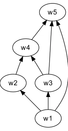
As an example, suppose that Σ={0,1}and the target circuit has a circuit graph as shown in Figure 2. There are four directed paths from w1to the output wire: w1w5, w1w3w5, w1w2w4w5and
w1w3w4w5. A w1-test path is a value injection experiment that sets the wires of one of these paths to ∗and the other wires to 0 or 1, for example,∗011∗or∗∗0∗∗. For the test path∗011∗, the side wires are w3 and w4, while for the test path∗∗0∗∗the side wire is w3. The value injection experiments ∗∗∗∗∗and∗01∗∗are not test paths.
A test path may help the learning algorithm determine the effects of assigning different values to the wire w. The test path lemmas (Angluin et al., 2008b, 2009) may be re-stated as follows.
Lemma 7 Let C be a deterministic circuit. If for some value injection experiment e, wire w free in
e and alphabet symbolsσandτit is the case that
C(p|w=σ) =C(p|w=τ)
for every test path p≤e then also
w1 w2 w3 w5
w4
Figure 2: A circuit graph; w5is the output wire.
Nontrivial complications arise in attempting to carry over this test path lemma to general proba-bilistic circuits, as we now show. The following lemma shows that for alphabets of size at least three, there are transitively reduced probabilistic circuits for which the test-path lemma fails completely.
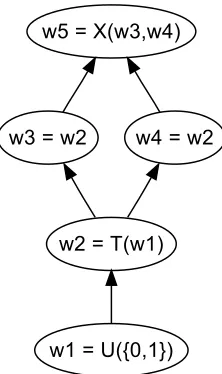
Lemma 8 If |Σ| ≥3, there exists a probabilistic circuit C, value injection experiment e, wire
w free in e and alphabet symbols σ and τ such that although for every test path p≤e for w, d(C(p|w=σ),C(p|w=τ)) =0, it is nevertheless the case that d(C(e|w=σ),C(e|w=τ)) =1/2.
Proof Assume thatΣ={0,1,2}, and define probabilistic gate functions T and X as follows.
T(0) =T(1) =U({0,1})
T(2) =2
X(b1,b2) =b1⊕b2if b1,b2∈ {0,1}
X(b1,b2) =U({0,1})if b1=2 or b2=2,
where⊕is sum modulo 2. The gate function T flips a coin on input 0 or 1, and passes 2 through unaltered. The gate function X is exclusive or if neither input is 2, and a coin flip otherwise.
The circuit C has 5 wires, connected as in Figure 3. The output wire is w5; note that C is transitively reduced.
Consider the experiment e that leaves all the wires free. In this experiment, we have C(e|w1=0) =
C(e|w1=1) =0 because w2is a coin flip and w5is the exclusive or of two copies of the coin flip. On
the other hand, C(e|w1=2) =U({0,1})because w4=w3=w2=2 and w5 is therefore a coin flip.
Thus d(C(e|w1=0),C(e|w1=2)) =1/2.
w1 = U({0,1}) w2 = T(w1) w3 = w2 w4 = w2
w5 = X(w3,w4)
Figure 3: The circuit C; w5is the output wire.
flip, and w5is the exclusive or of b and that coin flip, that is, w5is also coin flip. Hence, for any test path p≤e for w1, we have C(p|w1=0) =C(p|w1=2) =U({0,1})and d(C(pw1=0),C(pw1=2)) =0.
For alphabetsΣof size larger than 3, we can treat three of the symbols as 0, 1 and 2 in the above construction, and the other symbols as “tilt,” where each function outputs a tilt value if any of its inputs is a tilt value.
4.1 A Bound for Boolean Probabilistic Circuits
Surprisingly, the case of|Σ|=2 is different; for Boolean probabilistic circuits there is a useful quan-titative relationship between the difference exposed by an arbitrary experiment e and the differences exposed by test paths p≤e. The bound we give depends on the structure of directed paths on free
wires in e.
Let e be an experiment and w a wire. DefineΠ(e,w)to be the set of all directed paths from w to the output wire on free wires in e. Let S(e)be the set of wires that originate a free shortcut, that is, the set of free wires w such that there exists a path p∈Π(e,w)with two free wires to which w is an input. Define
κ(e,w) =
∑
p∈Π(e,w)2|p∩S(e)|.
Thus,κ(e,w)is the sum over paths inΠ(e,w) of 2 raised to the number of wires on the path that originate free shortcuts in e. If there are no wires that originate free shortcuts in e, then this is just the number of free paths in e. As an example, if the target circuit has the circuit graph shown in Figure 2 and the experiment e leaves all wires free thenΠ(e,w1)contains the four paths w1w5,
w1w3w5, w1w2w4w5and w1w3w4w5, S(e) ={w1,w3}, andκ(e,w)is 2+4+2+4=12. The following technical lemma gives a useful recurrence forκ(e,w).
Lemma 9 Let C be a probabilistic circuit, e be a distribution injection experiment, w and u be free
otherwise. Then
κ(e,w) =κ(e|u=D0,w) +κ(e|w=1,u)·β.
Proof The first term of the sum counts paths that don’t contain u, and the second counts paths that do. Let e′=e|u=D0 and e′′=e|w=1. We have
κ(e,w) =
∑
p∈Π(e,w)2|p∩S(e)|
=
∑
p∈Π(e,w)
u6∈p
2|p∩S(e)|+
∑
p∈Π(e,w)u∈p
2|p∩S(e)|
=
∑
p∈Π(e′,w)
2|p∩S(e′)|+
∑
p∈Π(e′′,u)2|p∩S(e′′)|β
=κ(e′,w) +κ(e′′,u)·β,
since each path p∋u from w corresponds to the path p\ {w}from u.
Next is the key lemma relating the difference exposed by e to the differences exposed by paths p≤e
for Boolean probabilistic circuits.
Lemma 10 Let C be a Boolean probabilistic circuit, e be a distribution injection experiment, w be
a wire free in e and D1,D2be value distributions. If there existsε≥0 such that for all w-test paths
p≤e,
d(C(p|w=D1),C(p|w=D2))≤ε,
then
d(C(e|w=D1),C(e|w=D2))≤κ(e,w)·ε.
Proof By induction onφ(e), the number of free wires in e. By Lemma 6, assume that support(D1)∩ support(D2) =/0. The critical feature of the Boolean case is that it follows that D1=0 and D2=1 without loss of generality—it is important to the following proof that D1and D2be deterministic.
Ifφ(e) =1, then either
d(C(e|w=0),C(e|w=1)) =0,
or w is the output, e is a w-test path, andκ(e,w) =1. Otherwise, the inductive hypothesis is that the lemma holds for all experiments e′withφ(e′)<φ(e).
Except for w, the experiments e|w=0and e|w=1agree on all constrained wires, so by Lemmas 4 and 5, assume without loss of generality that every wire with no free path from w is in fact fixed. Since C is acyclic, there exists a free wire u6=w whose only unfixed input is w. Let g be the gate
assigned by C to u and let B0=g(e|w=0)and B1=g(e|w=1), so that
C(e|w=0) =C(e|w=0,u=B0)
C(e|w=1) =C(e|w=1,u=B1).
By the triangle inequality,
d(C(e|w=0),C(e|w=1))≤d(C(e|w=0,u=B0),C(e|w=1,u=B0))
Letting e′=e|u=B0, any test path p≤e′also satisfies p≤e since e′≤e. The experiment e′has one
fewer free wire, as u is free in e, so using the inductive hypothesis, we can bound the first term of the sum byκ(e′,w)·ε. We now derive a bound on u-test paths so that the inductive hypothesis applies to the second term as well. Letβ=2 if w∈S(e)andβ=1 otherwise. Let e′′=e|w=1and suppose
p≤e′′is a u-test path. Then
d(C(p|u=B0),C(p|u=B1))
≤d(C(p|w=1,u=B0),C(p|w=0,u=B0)) +d(C(p|w=0,u=B0),C(p|w=1,u=B1))
[by the triangle inequality]
=d(C(p|w=1,u=B0),C(p|w=0,u=B0)) +d(C(p|w=0,u=∗),C(p|w=1,u=∗))
[by the definitions of B0and B1].
Since w is an input to u, both p|w=∗,u=B0 and p|w=∗,u=∗ are w-test paths. Therefore, both terms of
the sum are bounded byε, and the first is nonzero only if w is an input to some free wire in p other than u. It follows that
d(C(p|u=B0),C(p|u=B1))≤βε,
and thus that
d(C(e′′|u=0),C(e′′|u=1))≤κ(e′′,u)·βε,
so by Lemma 9,
d(C(e|w=0),C(e|w=1))≤κ(e′,w)·ε+κ(e′′,u)·βε
=κ(e,w)·ε.
In the case of transitively reduced circuits, S(e) =/0, andκ(e,w) =π(e,w), where π(e,w) = |Π(e,w)|, the number of directed paths on free wires in e from w to the output wire.
Corollary 11 Let C be a transitively reduced Boolean probabilistic circuit, e be a distribution
in-jection experiment, and w be a wire free in e. If there existsε≥0 such that for all w-test paths
p≤e,
d(C(p|w=0),C(p|w=1))≤ε,
then
d(C(e|w=0),C(e|w=1))≤π(e,w)·ε.
5. Learning Boolean Probabilistic Circuits
Theorem 12 Given constants c and k there is a nonadaptive learning algorithm that with
prob-ability at least(1−δ) successfullyε-approximately learns any Boolean probabilistic circuit with n wires, gates of fan-in at most k and depth at most c log n using value injection queries in time bounded by a polynomial in n, 1/εand log(1/δ).
The rest of the section is devoted to proving this theorem. Let the target circuit be C with
Σ={0,1}and let positive constantsδ,ε, k and c be given such that the fan-in of C is bounded by k and the depth of C is bounded by c log n. For such a circuit,π(e,w)is bounded above by kc log n, so the quantityκ(e,w)is bounded above by
κ(n) =kc log n·2c log n=nc(log k+1)=nO(1).
We now describe our Probabilistic Circuit Builder algorithm (PCB). PCB is nonadaptive: first it computes a set U of value injection experiments such that every test path is equivalent to some experiment in U . It then repeats each value injection query e∈U enough times that with probability
at least(1−δ), the distribution C(e)is estimated with sufficient accuracy for every e∈U . Finally,
it uses these estimates to build a circuit C′ by repeatedly adding a sufficiently accurate gate all of whose inputs are in the partially constructed circuit. If the estimates of C(e) are all sufficiently accurate, then C′ isε-behaviorally equivalent to C.
5.1 Constructing U
In choosing the experiments U , the goal is that for every potential test path, U includes an equiv-alent experiment. The structure of the circuit, however, is not known a priori, a difficulty that we overcome by the same method as used by Angluin et al. (2009). Let U∗be a universal set of value injection experiments such that for every set of kc log n wires and every assignment of symbols fromΣ∪ {∗}to those wires, some experiment e∈U∗agrees with the values assigned to those wires. There is a deterministic construction of such a set U∗of size
2O(kc log n)log n=nO(kc)
in time polynomial in its size (Angluin et al., 2009). (For intuition, a set of nO(kc) independent random uniform assignments of∗, 0 and 1 to the wires has this property with high probability.) For every wire w and test path p for w, there is an experiment in U∗that leaves the path wires of p free and fixes the side wires of p to their values in p. Consequently, p and this experiment agree on the output wire. In order to have experiments in which each free wire is also set to 0 and 1, for
b=0,1 let Ubcontain every experiment e|w=b such that e∈U∗ and w is free in e. The final set of
experiments is U=U∗∪U0∪U1.
5.2 Estimating C(e)for e∈U
For each e∈U , PCB repeatedly makes a value injection query with e to estimate the value
distribu-tion C(e); letCb(e)denote this estimate. By Hoeffding’s bound, we have that
m=O((nκ(n)/ε)2log(|U|/δ))
trials per experiment e suffice to guarantee that with probability at least 1−δ, for all e∈U ,
Let e∈U∗be a value injection experiment, w be a wire that e leaves free, and D be a value distribu-tion. We define
b
C(e|w=D) =
∑
σ∈Σ
D(σ)Cb(e|w=σ).
Note that this is computed from the values ofCb(e|w=σ)and does not require new experiments.
If (1) holds for all e∈U , then we have
d(C(e|w=D),Cb(e|w=D))≤
∑
σ∈Σ
D(σ)d(C(e|w=σ),Cb(e|w=σ))
≤ε/(4nκ(n)). (2)
5.3 Building the Circuit C′
PCB builds the circuit C′one gate at a time. Let W′ denote the set of wires of C′that have already been assigned a gate by PCB; initially W′ is empty. While W′6=W , PCB attempts to add another
gate to C′ by searching for a wire w∈(W−W′)and a probabilistic gate g′ all of whose inputs are in W′such that for each experiment e∈U∗that leaves w free and fixes all inputs of g′,
d(Cb(e),Cb(e|w=g′(e)))≤2ε/(4nκ(n)).
If no such gate can be found or W′=W , PCB outputs C′ and halts. We will later show that a gate can be found as long as W 6=W′.
The search for g′iterates over every wire w∈(W−W′)and every choice of an r-tuple of distinct wires w1, . . . ,wrfrom W′as the inputs of w, where 0≤r≤k. For each such choice, PCB attempts to define a probabilistic gate function f as follows. For each(σ1, . . . ,σr)∈Σr, PCB seeks a number
x∈[0,1]such that if Dxis the distribution that is 1 with probability x and 0 with probability(1−x) then
d(Cb(e),Cb(e|w=Dx))≤2ε/(4nκ(n))
for all experiments e∈U∗that leave w free and fix witoσifor i=1, . . . ,r. Since the left hand side is a convex function of x, every such e constrains the possible values of x to an interval, and any x in the intersection of[0,1]and the intervals for all such e suffices. If the intersection is empty, then the attempt to define f fails; otherwise, f(σ1, . . . ,σr)is defined to be Dx. If PCB succeeds in defining
f for all possible r-tuples(σ1, . . . ,σr), then the gate g′ with inputs w1, . . . ,wrand probabilistic gate function f is assigned to w.
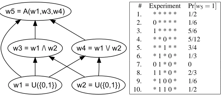
5.4 An Illustration
For some intuition about the operation of PCB, consider the probabilistic Boolean circuit shown in Figure 4. Wires w1and w2are determined by random coin flips, w3is the AND of w1and w2, w4is the OR of w1and w2, and w5is determined by the 3-input averaging gate applied to w1, w3and w4. The table shows the probability that w5=1 for a selected set of value injection experiments.
Suppose that these experiments are contained in U when PCB attempts to add the first gate to
w1 = U({0,1}) w2 = U({0,1})
w3 = w1 /\ w2 w4 = w1 \/ w2
w5 = A(w1,w3,w4) 1.# Experiment* * * * * Pr[1/2w5=1]
2. 0 * * * * 1/6 3. 1 * * * * 5/6 4. * * 0 * * 5/12 5. * * 1 * * 3/4 6. * 1 * 0 * 1/3 7. 0 1 * 0 * 0 8. 1 1 * 0 * 2/3 9. * 1 0 0 * 1/6 10. * 1 1 0 * 1/2
Figure 4: A Boolean circuit with output wire w5, and some of its behavior.
have no inputs and must be determined by a coin flip that is 1 with some probability x. In this group of experiments, there are two constraints for wire w1for the possible values of x. Experiments 1, 2 and 3 give the constraint(1/6)(1−x) + (5/6)x=1/2, which implies x=1/2, and experiments 6, 7 and 8 give the constraint 0(1−x) + (2/3)x=1/3, which also implies x=1/2, consistent with the gate computing w1in the target circuit. There are also two constraints on the possible values of
x for the wire w3. Experiments 1, 4 and 5 give the constraint(5/12)(1−x) + (3/4)x=1/2, which implies x=1/4, and experiments 6, 9 and 10 give the constraint(1/6)(1−x)+(1/2)x=1/3, which implies x=1/2. Thus there is no consistent value of x that would allow the first gate to be chosen for wire w3. Rather than exact values, PCB considers intervals determined by error tolerances, but when these are small enough, the constraint intervals for w3 will not overlap, and PCB will not choose the first gate for wire w3.
5.5 Correctness
With probability at least (1−δ), the estimatesCb(e) satisfy (1) for all e∈U . We now assume
that the estimates satisfy these bounds and show that PCB successfully builds a circuit C′ that is
ε-behaviorally equivalent to C.
We first establish two lemmas connecting gates, paths and experiments. Given a Boolean prob-abilistic circuit C and a probprob-abilistic gate g, g isη-correct for wire w with respect to C if for every value injection experiment e that fixes the input wires for g we have d(C(e),C(e|w=g(e)))≤η, where
g(e)denotes the value distribution determined by g when its inputs are fixed as in e. Recall thatφ(e) denotes the number of free wires in experiment e, and thereforeφ(e)≤n for all e.
Lemma 13 Let C and C′ be probabilistic circuits on wires W , and let e be a distribution injection experiment. If for every wire w, the gate for w in C′isη-correct for w with respect to C, then
d(C(e),C′(e))≤φ(e)·η.
Proof By induction onφ(e), the number of free wires in e. Ifφ(e) =0, then e constrains the output wire, and trivially, d(C(e),C′(e)) =0. Otherwise, the inductive hypothesis is that
for all experiments e′with fewer thanφ(e)free gates.
By Lemma 2, assume that e is in fact a value injection experiment. Since C′ is acyclic, there exists a free wire w in e such that the inputs to w in C′are fixed in e to some k-tuple(σ1, . . . ,σk)∈Σk. Let f denote the probabilistic gate function for w in C′, and let D denote the value distribution
f(σ1, . . . ,σk). Then we have C′(e) =C′(e|w=D), and
d(C(e),C′(e))≤d(C(e),C(e|w=D)) +d(C(e|w=D),C′(e|w=D)) ≤η+ (φ(e)−1)·η
=φ(e)·η
by the inductive hypothesis and the fact that f isη-correct for w.
Corollary 14 Let C and C′be probabilistic circuits on wires W where|W|=n. If for every wire w, the gate g for w in C′isη-correct for w with respect to C, then
d(C(e),C′(e))≤n·η.
Proof By the definition of approximate behavioral equivalence and the boundφ(e)≤n.
Next we show that test paths are sufficient to determine whether a gate isη-correct for a wire in
C.
Lemma 15 Let C be a Boolean probabilistic circuit, w a wire and g′ a probabilistic gate. If for every test path p for w that fixes all the inputs of g′, d(C(p),C(p|w=g′(p)))≤η/Kw, where Kwis the
maximum value ofκ(e,w)for C over all experiments e, then g′isη-correct for w with respect to C.
Proof Let g be the actual gate that C assigns to w. Let e be a value injection experiment that fixes every input of g′. Then e may not fix all of g’s inputs, but because C is acyclic, g’s inputs are not reachable from w. By Lemmas 4 and 5, there exists an experiment e′≤e that fixes g’s inputs, with
d(C(e′),C(e′|w=g′(e′)))≥d(C(e),C(e|w=g′(e))).
Since e′ fixes all of g’s inputs, C(e′) =C(e′|w=g(e′)). It is given that for all test paths p that fix all
inputs of g′that
d(C(p|w=g(p)),C(p|w=g′(p)))≤η/Kw,
so it follows by Lemma 10 that
d(C(e′|w=g(e′)),C(e′|w=g′(e′)))≤κ(e′,w)·η/Kw≤η,
and g′isη-correct for w.
Assume that W′6=W , that is, that not all wires have been assigned gates, and consider PCB as
it attempts to add another gate to C′. PCB looks for a wire w∈(W−W′) and probabilistic gate
g′∈G with all of its inputs in W′such that for each experiment e∈U∗that leaves w free and fixes all inputs of g′,
d(Cb(e),Cb(e|w=g′(e)))≤2ε/(4nκ(n)).
If this search succeeds, then by (1),
d(C(e),Cb(e))≤ε/(4nκ(n))d(Cb(e|w=g′(e)),C(e|w=g′(e)))≤ε/(4nκ(n)),
and thus by the triangle inequality we have
d(C(e|w=g′(e)),C(e))≤ε/(nκ(n)),
It follows by Lemma 15 and the choice ofκ(n)that g′isε/n-correct for w in C.
To see that the search for a gate will succeed as long as W′ 6=W , we note that because C is
acyclic, there is some wire w∈(W−W′)such that all of w’s inputs in C are in W′. Let g denote the gate assigned by C to w, with inputs w1, . . . ,wrand probabilistic gate function f . By the existence of g, there is at least one feasible gate-wire assignment for PCB to make, ensuring the continued progress of PCB. Consider any experiment e∈U∗ that leaves w free and fixes the inputs of g to (σ1, . . . ,σr). Let D be the value distribution f(σ1, . . . ,σr). Then C(e) =C(e|w=D)and by (1) and (2) we have
d(Cb(e),C(e))≤ε/(4nκ(n))
d(C(e|w=D),Cb(e|w=D))≤ε/(4nκ(n)),
so by the triangle inequality,
d(Cb(e),Cb(e|w=D))≤2ε/(4nκ(n)).
Therefore, PCB will continue to make progress until it has assigned a gate to every wire in W , and every such gate will beε/n-correct for its wire in C, which means that C′ will be ε-behaviorally equivalent to C.
5.6 Running Time
To bound the running time of PCB we argue as follows. The set U of experiments is of cardinality
nO(kc)and can be constructed in time polynomial in its size. To estimate C(e), each experiment in
U is repeated
O((nκ(n)/ε)2log(|U|/δ))
6. Lower Bounds on Path Attenuation
The path attenuation boundκ(n)is a significant factor in the running time of the PCB algorithm. In this section we consider lower bounds on path attenuation for Boolean probabilistic circuits. The following theorem shows that the bound of π(e,w) for transitively reduced Boolean probabilistic circuits in Corollary 11 is tight infinitely often.
Theorem 16 There is an infinite set of transitively reduced probabilistic Boolean circuits such that
for each circuit C in the family, there exists a value injection experiment e and a wire w free in e such that
d(C(e|w=0),C(ew=1)) =1
and for every test path p for w we have
d(C(p|w=0),C(p|w=1)) =1/π(e,w).
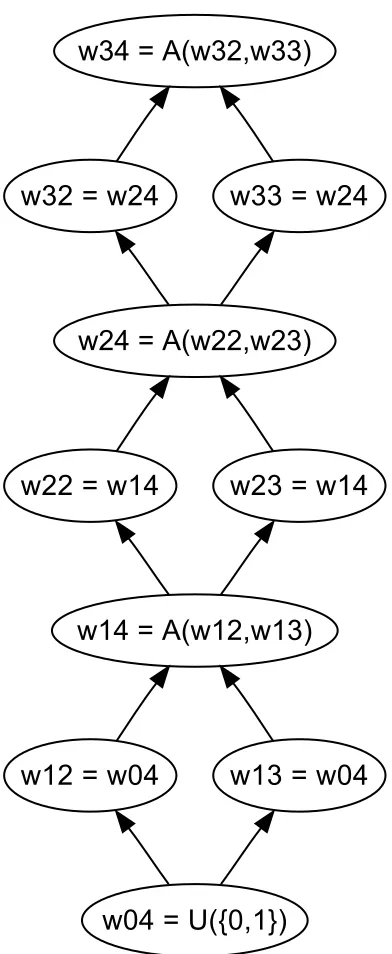
Proof For each positive integerℓ, define the circuit Cℓ to be a chain ofℓcopies of the circuit C1 in Figure 1 with wire w4of one copy identified with wire w1 of the next copy. More formally, the 3ℓ+1 wires are w0,4and wi,j for i=1, . . . , ℓand j=2,3,4. The output wire is wℓ,4. The wire w0,4 has no inputs and is determined by an unbiased coin flip, that is, U({0,1}). The wires wi,2and wi,3 are the outputs of deterministic identity gates with input wi−1,4. The wire wi,4=A(wi,2,wi,3)is the result of applying the two-input averaging probabilistic gate function A to the wires wi,2 and wi,3. The circuit C3is depicted in Figure 5.
To understand the operation of this circuit in response to a value injection experiment e, we may view each averaging gate as choosing one of its inputs to copy to its output. Starting at the output wire, this determines a path back to the first wire whose value has been fixed, or to the wire w0,4 (which has no inputs) and the output of the circuit is the value of the wire so reached.
Define experiment e to leave all of the wires free. Let w denote the wire w0,4. Clearly there are 2ℓ paths on free gates in e from w to the output gate, that is,π(w,e) =2ℓ. For experiment e every possi-ble path starts at wire w and we have C(e|w=0) =0 and C(e|w=1) =1, so d(C(e|w=0),C(e|w=1)) =1.
However, any test path p for w must fix one of the wires wi,2or wi,3for each i=1, . . . , ℓ. Thus, there is exactly one path that leads back to wire w, and this path is the one chosen by the averaging gates with probability 1/2ℓ. Thus the result for any test path p for w is d(C(p|w=0),C(p|w=1)) =1/2ℓ=
1/π(e,w).
This lower bound also holds for general transitively reduced circuit topologies, as follows. (Note that this result was incorrectly stated in the preliminary version of this paper (Angluin et al., 2008a).)
Theorem 17 Let G be a transitively reduced acyclic directed graph with a designated output node
z that is reachable from every node. For each node w there exists a Boolean probabilistic circuit C whose circuit graph is G with output wire z such that for every value injection experiment e that leaves w free and for every test path p≤e for wire w we have
d(C(e|w=1),C(e|w=0))≥π(e,w)·d(C(p|w=1),C(p|w=0)).
w04 = U({0,1})
w12 = w04
w13 = w04
w14 = A(w12,w13)
w22 = w14
w23 = w14
w24 = A(w22,w23)
w32 = w24
w33 = w24
w34 = A(w32,w33)
distinct directed paths from w to z that include node v, and for each edge(u,v), let P(u,v)denote the number of distinct directed paths from w to z that include edge(u,v). If there are no paths from
w to z through v (that is, P(v) =0) then we let the probabilistic gate function for v be the constant function 0. The probabilistic gate function for w is a coin flip, U({0,1}).
Otherwise, if node v has inputs u1, . . . ,ur then it is assigned the probabilistic gate function specified by
Av(b1, . . . ,br) = r
∑
i=1
bi·P(ui,v)/P(v)
This generalizes the two-input averaging gate A, weighting input ui by the fraction of paths from w to z passing through v that also pass through ui. We may view Avas performing a random weighted selection of one of its inputs to copy to its output. The weights have been chosen so that each directed path from w to z is selected with probability 1/P(w).
Let e be any value injection experiment that leaves w free. If there is no path on free wires in e from w to the output, thenπ(e,w) =0, and the bound in the conclusion of the lemma holds trivially. Otherwise, the output of the circuit in response to e is determined by tracing from the output wire, following the choices of the averaging gates, until either the first wire fixed by e, or w, is reached. Thus
d(C(e|w=1),C(e|w=0)) =π(e,w)/P(w),
because there areπ(e,w)paths from w to the output wire in e. Let p≤e be any test path for w; now
there is just one choice of path that leads back to w, so
d(C(p|w=1),C(p|w=0)) =1/P(w), establishing the conclusion of the lemma.
Can the general bound in Lemma 10 be improved to the bound for transitively reduced circuits in Corollary 11? The following example shows that the better bound is in general not attainable if the circuit is not transitively reduced. It gives a family of circuits of depth 2ℓfor which the worst-case ratio of the differences shown for w by an experiment e and the best path for w is(5/4)ℓπ(e,w).
Theorem 18 There exists an infinite set of Boolean probabilistic circuits D1,D2, . . .such that for
eachℓthere exists a value injection experiment e and a wire w free in e such thatπ(e,w) =4ℓand
d(Dℓ(e|w=0),Dℓ(e|w=1)) = (5/7)ℓ,
but for any test path p for w,
d(Dℓ(p|w=0),Dℓ(p|w=1)) = (1/7)ℓ.
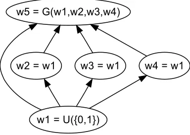
Proof We first define a Boolean probabilistic circuit D1 and then connectℓ copies of it in series to get Dℓ. The wires of D1 are w1, . . . ,w5. They are connected as in Figure 6; the output wire is
w1 = U({0,1})
w2 = w1 w3 = w1 w4 = w1
w5 = G(w1,w2,w3,w4)
Figure 6: The circuit D1; w5is the output wire.
function G is defined by giving its expected value as a function of its inputs:
E[G(w1,w2,w3,w4)] = ((1−w1) +2w2+2w3+2w4)/7. Let e be the experiment that leaves all five wires free. It is clear that
d(D1(e|w1=0),D1(e|w1=1)) =5/7.
We now show that for any test path p for w1,
d(D1(p|w1=0),D1(p|w1=1)) =1/7.
The possible test paths p for w1either fix all of w2,w3,w4or all but one of them. Thus, as we change from w1=0 to w1=1 in such a test path, the assignments to wires(w1,w2,w3,w4)change in one of four possible ways:
(0,b2,b3,b4)to(1,b2,b3,b4) (0,0,b3,b4)to(1,1,b3,b4) (0,b2,0,b4)to(1,b2,1,b4) (0,b2,b3,0)to(1,b2,b3,1)
Checking each of these possible changes against the definition of G, we see that each change pro-duces a difference of 1/7, as claimed. (This example can be modified to give a difference of 1 versus 1/5.) Thus, setting w=w1, the circuit D1gives the base case of the claim in the lemma.
To construct Dℓ, we takeℓcopies of D1 and identify wire w5 in one copy with wire w1in the next copy, making the wire w5of the final copy the output wire of the whole circuit. Let w denote the wire w1in the first such copy. Thenπ(e,w) =4ℓand
d(Dℓ(e|w=0),Dℓ(ew=1)) = (5/7)ℓ.
For any test path p, the signal is attenuated by a factor of 1/7 for each level, and we have
This construction can be generalized to k+1 wires for any odd k+1, which increases the attenuation. In the base circuit there are k paths and an attenuation factor of 1/(2k−3), and the worst-case ratio of differences for an experiment and its test paths in Dℓ approaches 2ℓπ(e,w)as k goes to infinity.
7. Exponential Dependence on Depth
The bounds on path attenuation show that test paths may be much less informative than general value injection experiments, resulting in the exponential dependence of the number of experiments and the running time of PCB on the depth of the target circuit. It is natural to ask whether we might do better by using selected general experiments. In this section, we give computational evidence to the contrary. The following result contrasts with the case of deterministic circuits, where the Distinguishing Paths algorithm uses value injection queries to learn arbitrary transitively reduced acyclic deterministic circuits of constant fan-in over polynomial size alphabets in polynomial time (Angluin et al., 2008b).
Theorem 19 If BPP6=NP and k≥4 then there is no polynomial time algorithm using value
injec-tion queries that approximately learns all acyclic transitively reduced Boolean probabilistic circuits with fan-in bounded by k.
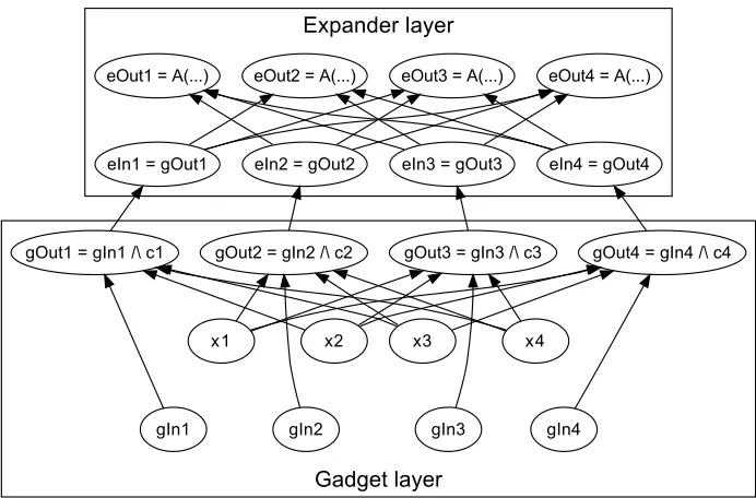
Proof Suppose L is a polynomial time algorithm that approximately learns the behavior of every transitively reduced acyclic Boolean probabilistic circuit of fan-in bounded by 4 using value in-jection queries. The hard computational problem we consider is the following: given a satisfiable 3-CNF formula φ over the variables x1, . . . ,xn with clauses c1, . . . ,cm, find an assignment to the variables that satisfies significantly more than seven-eights of the clauses of the formula. Finding such an assignment is NP-hard by a result of H˚astad (2001). We show how to transform the 3-CNF formulaφinto a pair of transitively reduced circuits C0 and C1 with maximum fan-in 4 such that value injection experiments show a difference that is exponentially small in the depth of the circuits unless we can find a variable assignment that satisfies significantly more than seven-eighths of the clauses of the formula.
The efficiency of our construction depends on the existence of a family of graphs with an ex-pansion property. Specifically, there exists a constantα<1 such that for sufficiently large m, there exists a directed graph Gm on m nodes with constant out-degree 3 such that the second largest eigenvalueλ2 of the transition matrix for a random walk on Gm satisfiesλ2≤α. Such a family can be constructed by the probabilistic method and explicit constructions are also known; these are surveyed by Hoory, Linial, and Wigderson (2006). Let r be the smallest integer such thatαr≤1/40. Letℓbe a positive integer. The two circuits C0and C1 differ only in their default assignments to a subset of their wires, so we describe their common structure as follows. The circuit consists of a stack ofℓrepetitions of a block consisting of r expander layers above one gadget layer for a total depth of(2r+1)ℓ. Figure 7 illustrates a block consisting of one expander layer (r=1) above a gadget layer. Recall that x1, . . . ,xnare the variables ofφand c1, . . . ,cmare the clauses ofφ.