†Corresponding Author: [email protected](S. S. Moosavi)
Tel/Fax: +98(0)9113204292
Address: Amol university of special modern technologies (AUSMT), AMOL, IRAN
Efficiency improvement and inrush current reduction in
a non-isolated DC-DC converter
S. S. Moosavi
1, †, H. Rezaee
2, A. Kazemi
3, A. Ranjbar
41 Clean power generation and Electrochemical laboratory, Amol university of special modern technologies
(AUSMT),IRAN
2,3 Kavosh institute of higher education, Mahmoudabad, IRAN
4 Babol Noshirvani University of technology, Babol, IRAN
DC–DC boost converters are unable to provide high step-up voltage gains due to the effect of power switches, rectifier diodes, and the equivalent series resistance of inductors and capacitors. A high step-up DC-DC converter based on the modified SEPIC converter is presented in this paper. Step up non-isolated converters generally suffer from problems such as high voltage stress and low efficiency. In this study, non-isolated boost converter structures, SEPIC, SEPIC modified circuit, and a proposed converter is studied. Then compare the performance of these typologies is located and presented as a chart. The operation analysis, design procedure for proposed converter is obtaied from 15V input voltage and 150V output voltage and with 100 watts output power. Using the proposed converter, the input inrush current and the invading voltage of the output have decreased. The time response analysis states that the proposed converter acts faster with deployment time than other converters.
Article Info
Keywords:
Boost converter, SEPIC converter, DC-DC power converter, non-isolated converter
Article History:
Received 2018-07-05
Accepted 2018-12-02
I.INTRODUCTION
Due to the limited fossil fuel sources and pollution caused by its use, the concept of using clean and renewable energy sources has been proposed in recent years. Photovoltaic systems with a clearer vision, high reliability, low operating cost, Eco-friendly and easier maintenance of renewable energy has been more attention [1]. One of the weaknesses of solar cells is the low efficiency (equivalent to 5 to 20 percent) that is directly converted into electricity [2]. The low voltage produced by the solar cells, the need for series and parallel to them, to reach a relatively high voltage in modules is mandatory Demand for high-static DC-DC converters for some applications, powered by a low voltage DC source such as renewable energy sources, fuel cells, embedded systems, portable electronic equipment, emergency power supplies and battery systems are ever increasing [3, 4]. When some loads
works with DC or AC voltage ratio higher than ten times the input source voltage, it is called a high voltage step [5].In order to achieve high voltage and increase the efficiency of systems, the use of high-power DC-DC converters is inevitable. Some of the problems of converting low voltage to high voltage are considered in the use of DC-DC converters include low input voltage, high inrush current and increased static gain. Boost converter, a non-isolated ordinary DC-DC converter with limited static gain and high voltage switching stress is used in ref. [6]. Despite the dependent elements same as the inductor and the capacitor in the converters, there is a limitation in increasing the voltage gain. The switch (MOSFET) is placed in a conventional boost converter under intense voltage stress, and the use of a high-level switch is inevitable and ultimately leads to high losses. Also, when the diode is reversed, a high voltage stress occurs in it [7, 8]. Although conventional SEPIC converter switch is more stress, but it can deliver the output with the same input polarity [9]. The modified SEPIC converter has twice the static gain compared to the normal boost converter, and the switching voltage is half the value of the output voltage [10-12]. In [12], A
a converter with a high static gain and reduced switching stress is proposed based on the design of the SEPIC converter. With faster deployment time and maximum output voltage in less time, reduces the input current to the inductor. In this paper, a DC-DC converter is provided by adding an inductor to the proposed converter [12]. Using the proposed converter, the input inrush current and the invading output voltage have been decreased. The time response analysis states that at in the input and output constant voltage, the proposed converter operates faster with deployment time than other converters considered in this paper. The structure of the paper is as follows: In section II, different structure of the DC-DC converter is shown. In section III, a new structure of DC-DC converter is proposed. In section IV, the simulation and results of the research are presented. Section V concludes this paper.
II. DC-DC CONVERTERS
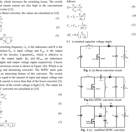
The Boost converter is a conventional step-up converter, which is used in high voltage applications. An example of this converter is shown in Figure 1(a) [12]. The boost converter switch is turned on for a long time because it use of the high duty cycle, which increases the switching losses. The switch stress and inrush current are also high in the conventional boost converter [13].
For the Boost converter, the values are calculated as [14]:
1 in out V D
V
= − (1)
1 in L V D L i f =
∆ (2)
o out out D C V R f V = ∆ (3)
f is the switching frequency, is the inductance and R is the load resistance. is input voltage and is the output voltage of the inverter. Capacitor , which is effective in reducing the output ripple. ∆ and ∆ are inductance current ripple and output voltage ripple respectively. Classic SEPIC conversion circuit is shown in Figure 1(b). Which is an increasing and decreasing converter. The SEPIC static gain range is an interesting feature of this converter. The switch voltage is equal to the amount of input and output voltage and the inrush current is lower than that of the boost converter [5], but the stress of the switch voltage is high [12]. The values for the SEPIC converter are calculated as [14]:
out out in
V
D
V
V
=
+
(4)1 1 in L V D L i =
∆ (5)
2 2 in L
V D
L
i
=
∆
(6)(
)
1 1/ C out D CR V V f
=
∆ (7)
(
)
0/
out outD
C
R
V
V
f
=
∆
(8) and are the inductors and and are capacitors of the SEPIC converter. The modification of the SEPIC converter is done by inserting the diode and the capacitor (Figure 1(c)). Many of the functional features of the SEPIC converter are changed with the proposed modifications. Capacitor is charged with the output voltage of classic boost converter. Therefore, the voltage applied to the inductor during the conduction of the power switch is greater than the classic SEPIC and increases static gain. Voltage polarity of the capacitor in the proposed converter is reversed [5] and [12]. The static gain doubles and the switching voltage drops to the half of the boost converter value. The inrush current flows at the start of the converter, in the inductor , and to reduce it, a large input inductor is required. This causes soft switching operation to switch on and off for all low input voltages. in the SEPIC converter, the Boost converter and the modified SEPIC (Figure 1(c)) converter is equal. Other values for the modified SEPIC (Figure 1(d)) converters are calculated as follows: out in out in V V D V V − =+ (9)
1 2 out L V D L L i f = =
∆ (10)
out s M c I C C V f = =
∆ (11)
0.1 1 in c V V D ∆ = −
(12) 0.1 is nominal capacitor voltage ripple.
Fig. 1. (a) Boost converter circuit
Fig.1(b) SEPIC converter circuit
Fig.1 (d) modified SEPIC converter
Fig. 1. (a) Boost converter circuit, (b) SEPIC converter
circuit, (c) and (d) modified SEPIC converter
In the modified SEPIC converter (Figure 1(d)), the inverse inrush current, the reverse voltage of the switches is lowered to the previous converters and the converter efficiency has increased, and the performance of the converter is faster than other previous converters. Eq. (8 to 11) also apply to this converter and the capacitors and are equal, and equal to half of the in (3). Overshoot voltage of this converter is its disadvantages.
III.PROPOSED DC-DC CONVERTER
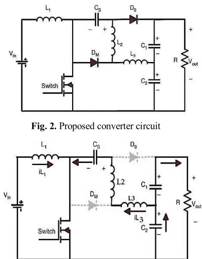
The proposed converter of this paper is shown in Figure 2. In this figure, the converter contains a switch, three inductors , and , two diodes and , and three capacitors , and . When the S switch is closed, bias diodes are reversed and turned off, as shown in Fig. 3. In this case, the inductors save energy. The current of and passes through capacitors and , and is parallel to the source. Figure 4 shows the switch when it is open. In this case, the diodes turn on and the inductor L1 is in discharge mode. The is discharged through the diode and through a capacitor . The total voltage of the capacitor and is equal to the output voltage of the converter. Voltage of capacitors and
is approximately equal (it is shown in Figure 6).
Fig. 2. Proposed converter circuit
Fig. 3. Proposed converter switched ON condition circuit.
The maximum voltage for the switch and all diodes are less than two thirds of the output voltage. The switching current in the ON mode is equal to the total current of the inductors L1 and L2 (see Figures 5-7).
1 2 out C C
V =V +V (13)
1 2
1
2
c c out
V
=
V
=
V
(14)Fig. 4. Proposed converter switched OFF condition circuit.
In this paper, the performance of a typical Boost, SEPIC and Modified SEPIC converter is investigated, because the proposed converter is derived from the modification in the structure of these converters. In the proposed converter, the conventional method has been used to obtain the inductor and capacitor calculation equations. The static gain of the proposed converter is determined by the fact that the mean voltage of the inductor in a steady state is zero. The amount of energy stored in the inductor is equal and symmetrical when the switch is on and/or off. The relationship between the duty cycle is provided in (16) with respect to the steady-state performance.
2 1 out
in
V D
V = −D
(15)
2 out out in
V D
V V
=
+ (16)
Fig. 5. Inductors current waveform in one cycle ON and OFF switch.
As seen in Figure 5, L1 and L2 inductor current ripple is quite similar, so:
1 2
1
in L DV
L L
f i
= =
∆
1 2 1 2 out out C out DV DV C C
Rf V Rf V
= = = ∆ ∆ (18) 1% out out V V ∆
= (19)
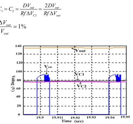
Fig. 6. Load voltage waveform, capacitors C1, C2 and the voltage on the switches.
Fig. 7. Current Waveforms of the inductors L1, L2 and the current passing through the switch.
The capacitor average current in one cycle is zero. So:
(
)
(
)
1
0.1 2 1
out s in i D C D fV − =
− (20)
(
)
20 2 1 s D C Rf D =− (21) Figure 7 shows that, in-time of the switched ON, the sum of the current flows of the inductors L1 and L2 with the current passing through the switch are equal. To calculate the components of the converters, the base values are shown in Table 1.
According to equation above, parametric values of the converters have been calculated as it is visible in Table 2.
Table 1. Base value of proposed converter
Table 2. Parameters and components of converters
Parameters
/components Boost SEPIC
Modified SEPIC c M o d if ie d S E P IC d p r o p o se e d Input voltage (Vin)
15 V 15 V 15 V 15 V 15 V
Switching frequency (f) 24 kHz 24 kHz 24 kHz 24 kHz 24 kHz Duty cycle
(D) 0.9 0.91 0.82 0.82 0.82
L1 112.5
µH 113.7 5 µH 102 µH 102 µH 102 µH
L2 - 113.7
5 µH 102 µH 102 µH 102 µH
C1 - 1.518 - 50
µF
50 µF
C2 - - - 50
µF 50 µF
Co 100
µF
100 µF
100
µF - -
Cs - - 3.37
µF
3.37 µF
3.37 µ F
CM - -
3.37
µF - -
R 224.88
Ω 224.88 Ω 224.88 Ω 224.88 Ω 224.88 Ω
IV.SIMULATION AND RESULTS
Proposed converter and other converters shown in Figure 1 is simulated using MATLAB/ Simulink to examine the design parameters above.
As shown in Figure 8, for the same input and output of all converters, the inrush current of the proposed converter is better than other converters in terms of both of the durability and the domain. Also, settling time of input current is faster in the proposed converter.
As shown in Figure 9, for the same input and output for all converters, the output voltage settling time of the proposed converter is faster. As shown in Figure 8 and 9, the proposed converter resulted in modification in the modified SEPIC converter (Figure 1(d)) in order to improve performance, increase the converter efficiency, reduce the intruder input current and decrease the settling time of the output voltage at the switching moment. The result is faster response of this converter than other converters studied. This converter works in combination of boost mode and SEPIC and reduces the inrush current in the inductor L1.
Switching frequency 24 kHz Output voltage 150 V
Fig. 8. Compare the inrush current of the studied converters
Fig. 9. Settling time the output voltage of the converters
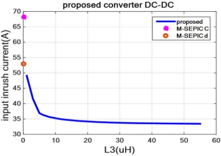
For compare the converters, the MATLAB Simulink is used. Initially, the effect of L3 on the characteristics of the proposed converter was examined and compared with the two converters the Modified SEPIC (Figure 1(c & d)). Two boost and SEPIC convert-ers have been discarded due to their large difference in their values compared to the other three converters. Also the difference between the duty cycles on these two con-verters, which makes it less efficient. Figure 10 shows the input inrush current. It is clearly that the proposed converter inrush current control is better. And by increasing the inductor L3, the inrush current is reduced.
However, it should be noted that reducing the amount of L3 will be effective up to a certain range. According to Figure 11, the inverse current ratio to the input current is shown for L3 changes. It is shown that L3=10 which is equivalent to 10% of the inductor L1, is a proper value.
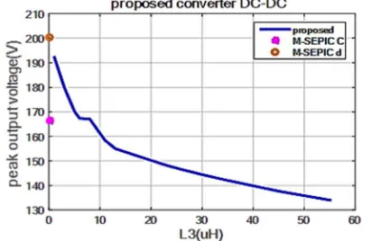
The effect of the inductor L3 on the proposed converter efficiency is shown in Figure 12. Increasing of the L3 value will increase the efficiency of the proposed converter. Even with a small amount of L3, it has better performance than other converters and it will lead to Reduces output voltage over shoot too (See Figure 13). It should be consider that the increase of the switch voltage is its disadvantages (See Figure 14). According to the stated contents, the value of the inductor L3 is suitable up to 10% of the inductor L1, and it brings good
results to us. Also the switch voltage is in suitable range (Less than two thirds of the output voltage).
Fig. 10. The effect of inductor L3 changes on the inrush input current of the proposed converter
Fig. 11. The effect of L3 inductance changes on the ratio of the input inrush current on its steady state flow
Fig. 12. The effect of L3 inductance changes on proposed converter efficiency and comparing it with two M-SEPIC-C,
Fig. 13. The effect of L3 inductance changes on the over-shooter of the proposed converter and comparing it with two
M-SEPIC-C, M-SEPIC-d
Fig. 14. The effect of L3 inductor changes on the inverse voltage of the proposed converter switch.
The output voltage of the boost, SEPIC, SEPIC C, M-SEPIC d, and the proposed converter in both L3 values (8 and 10 µH) are shown in Figure 15. The output voltage and current of the converters is shown in Figure. 15 and 16 under a stable performance with different duty cycles, and the lower voltage of the boost converter and SEPIC is visible to the modified converters and it shows that the modified converters voltage static gain is higher. In particular, it is in the range of 78% - 84% of the duty cycle used for increasing the voltage tenfold. In Figure 17, the changes of output voltage overshoot of converters are observed. The proposed converter performed better output voltage than the M-SEPIC-C and M-SEPIC-d converters. This will improve with increasing the inductor L3. It should be consider that a transient high output voltage can damage the load.
Fig. 15. Output voltage of DC-DC converter
Fig. 16. DC-DC converters output current
Table 3 shows the performance of the converters at 82% duty cycle where the input voltage is constant at 15 V . It is shown that the boost and SEPIC converter in this case have lower output voltage. To produce a voltage tenfold, the duty cycle of these two converters must be more than 90%.
However, the switching voltage of the SEPIC converter is very high but, the switching voltage on the converter is greater than the M-SEPIC-C and M-SEPIC-d which is within the permissible range. If necessary, this voltage can be reduced by reducing the amount of inductor L3. But the current of the proposed converter switch is almost equal to the modified converters and the boost and SEPIC converters due to the lower output voltage have less switching current. As it is shown in Figure 19, there is less input current for classic boost and SEPIC converter too. The current of other converters are almost equal to the input current due to the same output voltage. As shown in Figure 20, the proposed converter is very effective in controlling and reducing the inrush current.
Fig. 18. Switching voltage of DC-DC converters Fig. 19. DC-DC converters switching current
Table 3. Converter performance at 82% duty cycle for constant input voltage vaue of 15V
Fig. 20. Input peak current of DC-DC converters
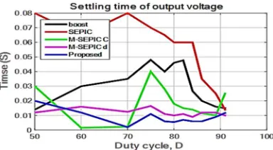
In Figure. 21, the time response of transient output voltage response has been analyzed for different types of converters. It is clear that the proposed converter is faster than other converters with settling time. For this reason, the proposed converter offers a faster response to the load and source voltage change.
In Figure 22, the efficiency change of different converters is shown. The proposed converter is in the best state of efficiency compared to other converters. The highest efficiency with 90.3 percent for the proposed converter has occurred in nominal values. The boost and SEPIC converters due to more duty cycle of switched ON (D = 90), have further switching losses and less efficiency.
Fig. 21. Settling time of output voltage
Fig. 22. Measured efficiency of the different converters
V. CONCLUSION
In this paper, a new structure of a non-isolated DC-DC converter with a high voltage static gain is presented. In this proposed converter, an inductor has been added, which reduces the input current. It is leaded to the reduce of tension at the output voltage. In addition to these features, the time response for the output voltage is improved by reducing the transient time and peak time. In full load conditions and whit inductor L3 = 10µH, the proposed converter is at the highest efficiency with 90.3% efficiency over other topologies presented by others and in the same conditions, the inrush current of the proposed converter is 37.6A that is18.7A less than the best converters in the previous works. The transient time of the output voltage in of the proposed converter is 5.4ms while for the best previous converter this time is was 10.6ms. This impresses on the speed of the system response to load changes. According to all said reasons, the proposed converter can be a good choice for many renewable energy systems applications with a simple design and high efficiency. Parameter/Components Boost SEPIC M-SEPIC-C M- SEPIC-d Proposed
L3=8
Proposed L3=10 Output voltage (V) 83.7521 112.948 150.8902 146.5836 147.167 146.8398 Switch voltage (V) 84.615 124.98 83.726 81.285 90.9 92.58 Inductor starting current (A) 59.38 26.78 69.32 54.5 37.4 37
REFERENCES
[1] Li, Q., & Wolfs, P. “A review of the single phase photovoltaic module integrated converter topologies with three different DC link configurations”, .IEEE Transactions on Power Electronics, 23(3), 1320–1333, 2008.
[2] Rekious, D., Matagne, E., “optimization of Photovoltaic Power Systems”, Springer-Verlag London Limited 2012, Springer book.
[3] Li, C W., He, X., “Review of Non-Isolated High Step-Up DC/DC Converters in Photovoltaic Grid-Connected Applications”, IEEE Transactions on Industrial Electronics, 58(4), 1239 – 1250, 2011.
[4] Wai, R. J., Duan, R. Y., “High-efficiency Power Conversion for Low Power Fuel Cell Generation System”, IEEE Transactions on Power Electronics, 20(4), 847-856, 2005.
[5] Gules, R., Dos Santos, W. M., Dos Reis, F. A., Romaneli, E. F. R., & Badin, A.A. “A modified SEPIC converter with high static gain for renewable applications”. IEEE Transactions on Power Electronics, 29(11), 5860–5871, 2014.
[6] Meneses, D., Blaabjerg, F., Garcia, O., & Cobos, J. A. “Review and comparison of step-up transformer less topologies for photovoltaic AC-module application”, IEEE Transactions on Power Electronics, 28(6), 2649–2663, 2013.
[7] Fathabadi, H., "Novel high efficiency DC/DC boost converter for using in photovoltaic systems", Solar Energy, 125, 22-31, 2016.
[8] Tseng, KC., Liang, TJ., "Novel high-efficiency step-up converter", IEE Proceedings, Electric Power Applications, 151(2), 182 – 190, 2004.
[9] Veerachary, M., "Power Tracking for Nonlinear PV Sources with Coupled Inductor SEPIC Converter”, IEEE Transactions on Aerospace and Electronic Systems, 41(3), 1019 – 1029, 2005.
[10] De Melo, P. F., Gules, R., Romaneli, E. F. R., & Annunziato, R. C., "A modified SEPIC converter for high-power-factor rectifier and universal input voltage applications", IEEE Transactions on Power Electronics, 25(2), 310–321, 2010.
[11] Yang, L. S., Liang, T. J., & Chen, J. F. "Transformer less DC–DC converters with high step-up voltage gain", IEEE Transactions on Industrial Electronics, 56(8), 3144–3152, 2009.
[12] Saravanan, S., Ramesh Babu, N., "A modified high step-up non-isolated DC-DC converter for PV application", Journal of Applied Research and Technology, 15(3), 242-249, 2017.
[13] Saravanan, S., Ramesh Babu, N.,”RBFN based MPPT algorithm for PV system with high step up converter”. Energy Conversion and Management, 122, 239-251, 2016. [14] Hart, D., Power Electronics - McGraw-Hill, ISBN
978-0-07-338067-4 (alk. paper) 2010.
Seyed Saeid Moosavi (S’09) was born in Amol, Iran. He received the B.Sc. degree in electrical power engineering, in 2004, the M.Sc. degree from the Electrical Railway engineering department of Iran University of science and technology (IUST), Tehran, Iran, in 2009. From 2007-2010 he was a researcher on Electrification, control and signaling of railway transportation He received the PHD in electrical engineering at university of technology Belfort Montbeliard, in 2013. He was assistant professor in the Systems and Transport (SET) laboratory at University of Technology Belfort Montbéliard, France and researcher in the FEMTO-ST laboratory in 2014. Now he is assistant profsor of Amol university of special modern technologies. His main research interests include the modeling of electrical machines (EM), hybrid/electric vehicle (H/EV) and the study and application of, condition monitoring, signal processing, fault detection and diagnosis techniques for EM and H/EV.
Hossein Rezaei received the B.Sc. degree in power electrical from Babol Noshirvani university of Technolgy-Iran in 1999. He currently a M.SC. student in the Power Electrical Department of Kovosh Institute -Iran. His current research interests Power Quality and power electronic.
Asadollah Kazemi received his B.Sc. from Tabriz university-Iran in 1990. His MS from Tehran-Iran in 1998 and his Ph.D from UKM university- Malaysia in 2013. He currently is an assistant professor at the Power Electrical Department of Kovosh Institute -Iran. His current research interests Power Quality, Reactive Power Control and Renewable Energy.