Low Power Optimization Of Full Adder, 4-Bit Adder
And 4-Bit BCD Adder
Y L V Santosh Kumar, U Pradeep Kumar, K H K Raghu Vamsi
Abstract: Micro-electronic devices are playing a very prominent role in electronic equipments which are used in daily life. For electronic equipment battery life is important. So, in order to reduce the power consumption we implement a Sleepy technique to the electronic circuits. Sleepy technique is also called as power gating technique. In the power gating structure, a circuit operates in two different modes. In the sleep mode, the sleep transistors are turned OFF to reduce the leakage power. In the active mode, the sleep transistors are turned ON and can be treated as the functional redundant resistances, as circuit is in operation mode the power leakage should not be more than the basic full adder. When a sleepy transistor is placed at VDD, it
is called as the "Header switch" and while it is placed near the ground, it is called as "Footer switch". Now in our project we implement this technique to the Full-adder and then it is used in 4-Bit Adder and 4-bit BCD Adder using 90nm scale technology. Without losing the CMOS logic a new full adder is designed by reducing the number of transistors which also leads to the reduction of chip size. In almost all electronic equipment full adder is used. So this project has been done with the aim of reducing the power consumption in the full adder circuit and implementing it in 4-Bit Adder and 4-Bit BCD Adder.
Index Terms: Power gating, Sleep transistor, Header switch, Footer switch, Full Adder, 4-Bit Adder, 4-Bit BCD Adder
————————————————————
1
I
NTRODUCTIONElectronic devices such as mobile phones, cameras are used commonly these days. Its battery life span is of great concern. When mobile phone is operated in standby mode, certain programs of mobile phone or camera are turned off during active or talk mode but this doesn't stop the battery from getting depleted. This is because circuits which are de-activated by turning off certain programs still have leakage currents flowing through them. Even though the magnitude of leakage current is lesser than the normal operating current but leakage current erodes battery life over relatively long standby time whereas the normal operating current erodes battery life over relatively short talk time. Thus this is why low power circuits for mobile applications are of great interest. Implementation of adder cells to reduce the power consumption and to increase the speed has proved to be a worthy solution towards power reduction. Moreover, realization of adders with different approaches using CMOS technology widens the area of power reduction, performance of the adder cells can be evaluated by measuring the factors such as leakage power, active power in context to voltage and transistor scaling. Reducing the transistor's gate length when no voltage is applied at gate results in more leakage current between source and drain of the transistor which eventually results in the more power consumption.
2 P
ROPOSEDF
ULLA
DDERC
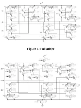
IRCUITSTo minimize the number of transistors required to implement a given logic function can be done by pseudo NMOS and Pass-transistor but they result in more static power dissipation whereas on the other hand, dynamic logic style needs small silicon area for the implementation of complex function but charge leakage and charge refreshing reduces the operating frequency. In general, none of the mentioned styles can beat the CMOS style. The conventional CMOS adder has been shown in Figure: 1, it is the basic adder and all simulation results comparison has been done with it.
Figure 1: Full adder
Figure 2: Sleepy Full Adder
transistor between actual ground rail and circuit ground (virtual ground). Here low leakage NMOS is used as a sleep transistor. The width for NMOS is kept as 0.27um whereas for PMOS it's 0.54um and length is fixed for both i.e., 90nm as 90nm scale technology is used in this project. Sub threshold current is directly proportional to W/L ratio of transistor so the sizing reduces the standby leakage current to a very great extent. Adder design shown in Fig.2 is Sleepy Full Adder and Sleepy Keeper Full Adder in Fig.3 as the drawback in sleepy technique is avoided by using sleepy keeper technique without any change in power dissipation. In active mode the dissipation of power of circuit is active power. This active power consists of dynamic power as well as the static power so it is being named as an active power. It is measured by making both the header and footer switches ON and then giving input vectors to the circuit and then the average power dissipation is calculated, then the results are compared as shown in Table-1. In static mode, since both the header and footer switches will be OFF, there will no Vdd supply and ground connected to the
circuit, so the power dissipation will be very less, i.e., sub threshold leakage current will be present.
Figure 3: Sleepy Keeper Full Adder
The major drawback in Sleepy technique is that it can’t retain the values when it enters into sleep mode that is static mode, since there will be no supply the output values can’t be retained. For combinational circuits it may be fine but for sequential techniques it will fail as they depend on previous outputs and sleepy technique can’t do it, so in order to avoid this discrepancy we go for Sleepy Keeper. In Sleepy Keeper technique in addition to sleep transistors another two transistors will be connected to retain the value in sleep mode as shown in the Figure-3. And the power dissipation will have no effect when compared to sleepy technique as shown in Table-1, so this technique is preferred over sleepy technique.
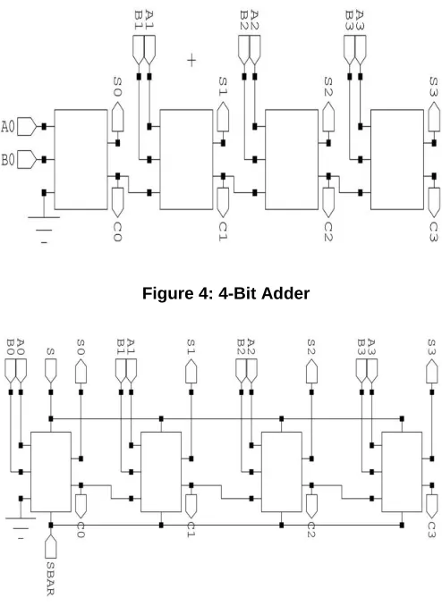
2.1 PROPOSED 4-BIT ADDER
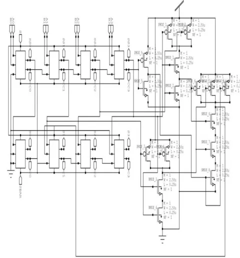
By using the full adders designed above, 4-Bit Adder is designed. The design shown in Figure-4, is designed by using basic full adder (Figure-1). The design shown in Figure-5 is similar for both sleepy and sleepy keeper technique but the
Figure 4: 4-Bit Adder
Figure 5: Sleepy or Sleepy Keeper 4-Bit Adder
2.2 PROPOSED 4-BIT BCDADDER
Figure 6: 4-Bit BCD Adder
Figure 7: 4-Bit BCD Adder
Figure 8: Sleepy or Sleepy Keeper 4-Bit BCD Adder
3
S
IMULATIONR
ESULTS3.1PERFORMANCE ANALYSIS
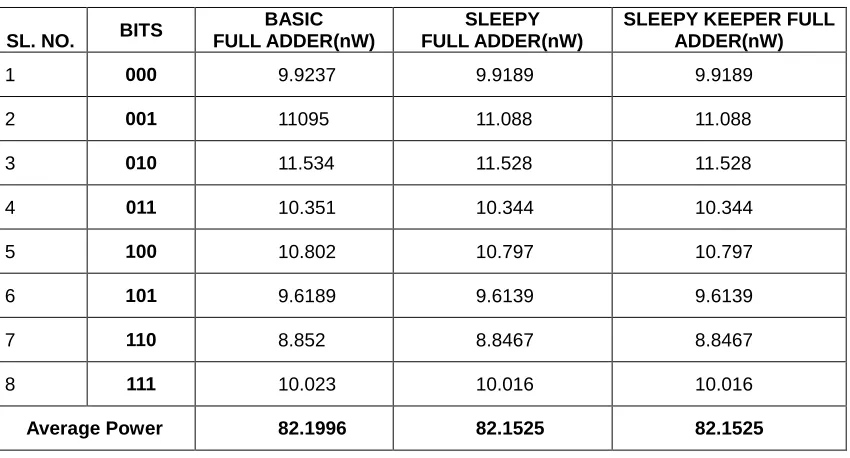
TABLE 1
COMPARISON OF STATIC POWER OF FULL ADDERS
SL. NO. BITS BASIC
FULL ADDER(nW)
SLEEPY
FULL ADDER(nW)
SLEEPY KEEPER FULL ADDER(nW)
1 000 9.9237 0.25249 0.26451
2 001 11095 0.24805 0.25772
3 010 11.534 0.25059 0.26086
4 011 10.351 0.2308 0.23992
5 100 10.802 0.25057 0.26083
6 101 9.6189 0.23068 0.23979
7 110 8.852 0.22630 0.23439
8 111 10.023 0.22002 0.22203
Average Power 82.1996 1.9095 1.98005
TABLE 2
COMPARISON OF ACTIVE POWER OF FULL ADDERS.
SL. NO. BITS
BASIC FULL ADDER(nW)
SLEEPY FULL ADDER(nW)
SLEEPY KEEPER FULL ADDER(nW)
1 000 9.9237 9.9189 9.9189
2 001 11095 11.088 11.088
3 010 11.534 11.528 11.528
4 011 10.351 10.344 10.344
5 100 10.802 10.797 10.797
6 101 9.6189 9.6139 9.6139
7 110 8.852 8.8467 8.8467
8 111 10.023 10.016 10.016
TABLE 3
POWER ANALYSIS OF DIFFERENT TECHNIQUES
Circuit Basic CMOS
Technique Sleepy Technique
Sleepy Keeper Technique
Full adder 82.1996 82.1525 82.1525
4-Bit Adder 39.929 39.910 39.910
4-Bit BCD Adder 82.059 82.024 82.024
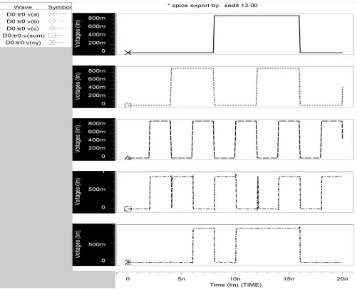
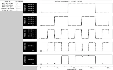
3.2SIMULATED WAVEFORMS
4
C
ONCLUSIONIn this paper 1-bit full adder cell with Sleepy technique is implemented where a sleep transistor is added between actual ground rail and circuit ground. The device is turned off during sleep mode to cut-off the leakage path. For optimal performance, Sleepy Keeper technique has been implemented. The comparison of static and active power is done and it’s observed that power is reduced as we move from conventional CMOS full adder cell to Sleepy and to Sleepy Keeper technique in both modes. The implemented 1-bit full adders are designed using 90nm technology. So, from this we would like to propose the sleepy keeper technique for digital circuits for efficient performance of the device and for good battery life.
R
EFERENCES[1] Rabaey J. M., A. Chandrakasan, B. Nikolic, Digital Integrated Circuits, A Design Perspective, 2nd Prentice Hall, Englewood Cliffs, NJ, 2002
[2] Pren R. Zimmermann, W. Fichtner, ―Low-power logic styles: CMOS versus pass-transistor logic,‖ IEEE J. Solid- State Circuits, vol. 32, pp. 1079–1090, July 1997.
[3] S.G.Narendra and A. Chandrakasan, Leakage in Nanometer CMOS Technologies. New York: Springer-verlag, 2006.
[4] K.Bernstein et al., ―Design and CAD challenges in sub- 90nm CMOS technologies,‖ in Proc. int. conf. comput. Aided Des.,2003, pp.129-136. A. Karnik, ―Performance of TCP congestion control with rate feedback: TCP/ABR and rate adaptive TCP/IP,‖ M. Eng. thesis, Indian Institute of Science, Bangalore, India, Jan. 1999.
[5] S.Mutoh et al., ―1-v power supply high-speed digital circuit technology with multithreshold-voltage CMOS.‖JSSC, vol.SC- 30, pp.847-854, Aug.1995.
[6] Abdullah A, Fallah F, and Pedram M, (Jan. 2007) "A robust power-gating structure and power mode transition strategy for MTCMOS design" IEEE Trans. Very Large Scale Integr. (VLSI) Syst., Vol. 15, No.1, pp. 80-89
[7] Chang H, Lee C, and Sapatnekar S.S, (2005) "Full chip analysis of leakage power under process variations, including spatial correlations" in Proc. es. Autom. Coni (DAC), pp. 523-528
[8] Chen Y.T, Juan L.C, Chang S.C, (2007) "An efficient wake-up schedule during power modetrans. ItI On considering spurious glitches phenomenon" in Proc. Int. Coni Comput.-Aided Des. (ICC AD), pp. 777-782.
[9] Designing Low-Power Circuits: Practical Recipes by Luca Benini Giovanni De Micheli Enrico Macii. and Howard D, Shi K (2006), "Sleep transistor design and implementation Simple concepts yet challenges to be optimum" in Proc. VLSI-DAT, pp. 1-4
[10] Pan Z.D, Ramalingam A, Devgan A, (Apr 2007) "Wake-up scheduling in MTCMOS circuits using successive relaxation to millimize ground bounce" ASP J. Low Power Electron. (JOLP), Vol. 3, No. 1.
A
UTHORSY L V Santosh Kumar is pursuing his M.Tech (VLSI-SD) in Pydah College of Engineering and Technology. His areas of interest include design of Low power circuits.
U Pradeep Kumar completed his M.Tech (VLSI-SD) in Avanthi College of Engineering and Technology. He is working as Assistant Professor in Pydah College of Engineering and Technology. His areas of interest include design of Low power circuits.