1518 | P a g e
RENEWABLE POWER GENERATION SYSTEM
USING 5-LEVEL AND 9-LEVEL INVERTERS
S. Siva Prasad
1, A.B Bhavana Reddy
21
Professor ,
2Assistant Professor, Dept of EEE,
Vidya Jyothi Institute of Engineering and Technology, Hyderabad
ABSTRACT
In this paper, a multi-level inverter is developed and applied for injecting the real power of the renewable power intothe grid to reduce the switching power loss, harmonic distortion, and electromagnetic interference caused by the switching operation of power electronic devices. Here a dual buck configuration with full bridge inverter is used for the MLI implementation. The input of the dual-buck converter is dc capacitor voltage sources. The output voltage of the dual-buck converter supplies to the full-bridge inverter. The power electronic switches of the full-bridge inverter are switched in low frequency synchronous with the utility voltage to convert the output voltage of the dual-buck converter to a multi-level ac voltage. The output current of the multi-level inverter is controlled to generate a sinusoidal current in phase with the utility voltage to inject into the grid. Five level and nine level topologies are developed to verify the performance of the developed renewable power generation system. The simulation results show that the developed renewable power generation system reaches the expected performance with the help of proposed topology.
Keywords: Harmonic Distortion, Inverters, Power Electronics.
I. INTRODUCTION
The conventional single-phase inverter topologies for grid connection include half-bridge and full bridge [1]–
[4]. The half-bridge inverter is configured by one capacitor arm and one power electronic arm. The dc bus
voltage of the half-bridge inverter must be higher than double of the peak voltage of the output ac voltage. The
output ac voltage of the half-bridge inverter is two levels. The voltage jump of each switching is the dc bus
voltage of the inverter. The full-bridge inverter is configured by two power electronic arms. The popular
modulation strategies for the full-bridge inverter are bipolar modulation and unipolar modulation [3], [5]. The dc
bus voltage of the full-bridge inverter must be higher than the peak voltage of the output ac voltage. The output
ac voltage of the full-bridge inverter is two levels if the bipolar modulation is used and three levels if the
unipolar modulation is used. The voltage jump of each switching is double the dc bus voltage of the inverter if
the bipolar modulation is used, and it is the dc bus voltage of the inverter if the unipolar modulation is used. All
power electronic switches operate in high switching frequency in both half-bridge and full bridge inverters. The
switching operation will result in switching loss. The loss of power electronic switch includes the switching loss
and the conduction loss. The conduction loss depends on the handling power of power electronic switch. The
1519 | P a g e power electronic switches. The power efficiency can be advanced if the switching loss of the dc–ac inverter is
reduced. Multilevel inverter can effectively reduce the voltage jump of each switching operation to reduce the
switching loss and increase power efficiency. The number of power electronic switches used in the multilevel
inverter is larger than that used in the conventional half-bridge and full-bridge inverters. Moreover, its control
circuit is more complicated. Thus, both the performance and complexity should be considered in designing the
multilevel inverter. However, interest in the multilevel inverter has been aroused due to its advantages of better
power efficiency, lower switching harmonics, and a smaller filter inductor compared with the conventional
half-bridge and full-half-bridge inverters.
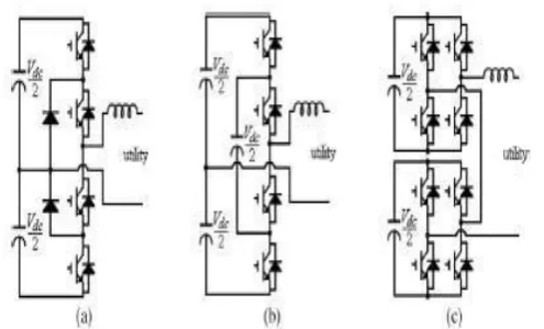
Fig. 1. Circuit configuration of conventional single phase multilevel inverter.(a) Diode clamped. (b) Flying
capacitor. (c) Cascade H-bridge
The conventional single-phase multilevel inverter topologies include the diode-clamped, the flying capacitor,
and the cascade H-bridge types, as shown in Fig. 1. Fig. 1(a) shows the basic configuration of a diode-clamped
multilevel inverter. Fig. 1(b) shows the circuit configuration of a basic flying capacitor multilevel inverter. As
can be seen, it is configured by three dc capacitors and four power electronic switches. The voltage on each dc
capacitor is controlled to be Vdc/2, and the output voltage of the basic flying capacitor multilevel inverter has
three levels. The voltage difference of each level is also Vdc/2 (the voltage on a dc capacitor).These three dc
capacitors must be controlled for maintaining their voltages to be Vdc/2 in the charge and discharge processes.
Therefore, its control circuit is more complicated. If five-level output voltage is required, an extra dc capacitor
and four power electronic switches are required [1], [6], [5]. Fig. 1(c) shows the circuit configuration of the
basic cascade H-bridge multilevel inverter [4]–[1], [5], [2]. As can be seen, it is configured by two full-bridge
inverters connected in cascade. The dc bus voltage of each full-bridge inverter is Vdc/2, and the output voltage
of each full-bridge inverter can be controlled to be Vdc/2, 0, and −Vdc/2. Thus, the voltage levels of the output
voltage of the cascade full-bridge multilevel inverter are Vdc, Vdc/2,0, −Vdc/2, and −Vdc. This topology has
advantages of fewer components being required compared with other multilevel inverters under the output
voltage with the same levels, and its hardware circuit can be modularized because the configuration of each full
bridge is the same. However, this topology has the disadvantages that two independent dc voltage sources are
required. In this paper, a five/nine-level inverter is developed and applied for injecting the real power of the
renewable power into the grid. The power electronics witches of the dual-buck converter are switched in high
1520 | P a g e switches of the full-bridge inverter are switched in low frequency synchronous with the utility to convert the
output voltage of the dual-buck converter to a five/nine-level ac voltage. Therefore, the switching power loss,
harmonic distortion, and electromagnetic interference (EMI)caused by the switching operation of power
electronic devices can be reduced, and the control circuit is simplified. Besides, the capacity of output filter can
be reduced. In this paper five level inverter is developed by using one dual buck converter with full bridge
inverter configuration. To provide five level output two dc capacitors are implemented. In the below sections
five level implementation is explained. The same will be provided for nine level also , but in the circuit
configuration two switches and two capacitors are going to increase in dual buck converter and both the results
of five and nine level inverter are as shown in the simulation results.
II. CIRCUIT CONFIGURATION
Fig. 2 shows the circuit configuration of the five-level inverter applied to a photovoltaic power generation
system. As can be seen, it is configured by a solar cell array, a dc–dc converter, a five-level inverter, two
switches, and a digital signal processor (DSP)-based controller. Switches SW1 and SW2 are placed between the
five-level inverter and the utility, and they are used to disconnect the photovoltaic power generation system
from the utility when islanding operation occurs. The load is placed between switches SW1 and SW2. The
output of the solar cell array is connected to the input port of the dc–dc converter. The output port of the dc–dc
converter is connected to the five-level inverter. The dc–dc converter is a boost converter, and it performs the
functions of maximum power point tracking (MPPT) and boosting the output voltage of the solar cell array. This
five-level inverter is configured by two dc capacitors, a dual buck converter, a full-bridge inverter, and a filter.
The dual-buck converter is configured by two buck converters. The two dc capacitors perform as energy buffers
between the dc–dc converter and the five-level inverter. The output of the dual-buck converter is connected to
the full-bridge inverter to convert the dc voltage to ac voltage. An inductor is placed at the output of the full
bridge inverter to form as a filter inductor for filtering out the high-frequency switching harmonic generated by
the dual-buck converter.
III. OPERATIONPRINCIPLE OFFIVE-LEVEL INVERTER
The operation of this five-level inverter can be divided into eight modes. Modes 1–4 are for the positive
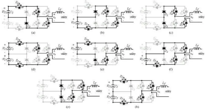
half-cycle, and modes 5–8 are for the negative half-cycle. Fig. 3 shows the operation modes of five-level inverter. As
can be seen, the power electronic switches of the full-bridge inverter are switched in low frequency and
synchronously with the utility voltage to convert the dc power into ac power for commutating. As seen in Fig.
3(a)–(d), the power electronic switches S4 and S7 are in the ON state, and the power electronic switches S5 and
S6 are in the OFF state during the positive half-cycle. On the contrary, the power electronic switches S4 and S7
are in the OFF state, and the power electronic switches S5 and S6 are in the ON state during the negative
half-cycle. Since the dc capacitor voltagesVC2 and VC3 are balanced by controlling the five-level inverter, the dc
capacitor voltages VC2 and VC3 can be represented as follows:
1521 | P a g e Mode 1: Fig. 3(a) shows the operation circuit of mode 1.Thepower electronic switch of the dual-buck converter
S2 is turned ON and S3 is turned OFF. DC capacitor C2 is discharged through S2, S4, the filter inductor, the
utility, S7, and D3 to form a loop. Both output voltages of the dual-buck converter and five-level inverter are
Vdc/2.
Mode 2: Fig. 3(b) shows the operation circuit of mode 2.Thepower electronic switch of the dual-buck converter
S2 is turned OFF and S3 is turned ON. DC capacitor C3 is dischargedthroughD2, S4, the filter inductor, the
utility, S7, and S3 to forma loop. Both output voltages of the dual-buck converter and five level inverter are
Vdc/2.
Mode 3: Fig. 3(c) shows the operation circuit of mode 3.Both power electronic switches S2 and S3 of the
dual-buck converter are turned OFF. The current of the filter inductor flows through the utility, S7, D3, D2, and S4 .
Both output voltages of the dual buck converter and five-level inverter are 0.
Fig. 2. Circuit configuration of the developed photovoltaic power generation system.
Fig. 3. Operation modes of the five-level inverter. (a) Mode 1. (b) Mode 2. (c) Mode 3. (d) Mode 4. (e)
Mode 5. (f) Mode6. (g) Mode 7. (h) Mode 8.
1522 | P a g e Mode 4: Fig. 3(d) shows the operation circuit of mode 4.Both power electronic switches S2 and S3 of the
dual-buck converter are turned ON.DCcapacitorsC2 andC3 are discharged together through S2, S4, the filter
inductor, the utility, S7 , and S3 to forma loop. Both output voltages of the dual-buck converter and five-level
inverter are Vdc.
Modes 5: 8 are the operation modes for the negative halfcycle. The operations of the dual-buck converter under
modes5–8 are similar to that under modes 1–4, and the dual-buck converter can also generate three voltage
levels Vdc/2, Vdc/2, 0,and Vdc, respectively. However, the operation of the full-bridge inverter is the opposite.
The power electronic switches S4 andS7 are in the OFF state, and the power electronic switches S5 andS6 are in
the ON state during the negative half-cycle. Therefore, the output voltage of the five-level inverter for modes 5–
8 will be −Vdc/2, −Vdc/2, 0, and −Vdc, respectively. Considering operation modes 1–8, the full-bridge inverter
converts the dc output voltage of the dual-buck converter with three levels to an ac output voltage with five
levels which are Vdc, Vdc/2, 0, −Vdc/2, and −Vdc.
IV. VOLTAGE BALANCE OF FIVE-LEVEL INVERTER
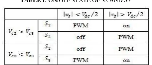
Balancing the voltages of dc capacitors is very important in controlling the multilevel inverter. The voltage balance of
DC capacitor voltages VC2 and VC3 can be controlled by the power electronic switches S2 and S3 easily. When the
absolute of the utility voltage is smaller than Vdc/2, one power electronic switch either S2 or S3 is switched in high
frequency and the other is still in the OFF state. Which power electronic switch is switched in high frequency depends
on the dc capacitor voltages VC2 andVC3. If dc capacitor voltage VC2 is higher than dc capacitor voltage VC3,
power electronic switch S2 is switched in high frequency. In this situation, the voltage source is VC2, and
C2 will be discharged. Thus, the dc capacitor voltagesVC2 decreases and VC3 does not change. On the
contrary, power electronic switch S3 is switched in high frequency when voltageVC3 is higher than voltage
VC2. In this situation, the voltage source VCx is VC3. Thus, the dc capacitor voltagesVC3 decreases and VC2
does not change. In this way, the voltage balance of C2 and C3 can be achieved. When the absolute of the utility
voltage is higher than Vdc/2, one power electronic switch either S2 or S3 is switched in high frequency and the
other is still in the ON state. Which power electronic switch is switched in high frequency depends on the dc
capacitor voltages VC2 and VC3. If dc capacitor voltage VC2is higher than dc capacitor voltage VC3 , the
power electronic switch S3 is switched in high frequency. The voltage source VCx
TABLE I: ON/OFF STATE OF S2 AND S3
is dc capacitor voltage VC2 . When the power electronic switch S3 is turned ON, both C2 and C3 are
discharged. However, only C2 supplies the power when the power electronic switch S3 is turned OFF. Thus, C2
will discharge more power than that of C3. On the contrary, the power electronic switch S2is switched in high
1523 | P a g e dc capacitor voltage VC3. When the power electronic switch S2 is turned ON, both C2 and C3 are discharged.
However, only C3 supplies the power when the power electronic switch S2 is turned OFF. Thus, C3 will
discharge more power than that of C2. In this way, the voltage balance of C2 and C3can be achieved. As
mentioned earlier, the operation of power electronics witches S2 and S3 can be summarized as Table I. The
voltages of capacitors C2 and C3 can be easily balanced compared with the conventional multilevel inverter.
V. CONTROL BLOCK DIAGRAM
The developed photovoltaic power generation system consists of a dc–dc power converter and the five-level
inverter. The five-level inverter performs the functions of converting the dc power into high-quality ac power
and injecting it into the utility ,balancing two dc capacitor voltages VC2 and VC3 , and detecting the islanding
operation. The dc–dc converter boosts the output voltage of the solar cell array and performs the MPPT to
extract the maximum output power of the solar cell array. The controllers of both the dc–dc converter and the
five-level inverter are explained as follows.
5.1. Five-Level Inverter
Fig. 4 shows the control block diagram of five-level inverter. In the operation of the five-level inverter, the dc
bus voltage must be regulated to be larger than the peak voltage of the utility and the dc capacitor voltages of C2
and C3 must be controlled to be equal. Besides, the five-level inverter must generate a sinusoidal current in
phase with the utility voltage to be injected into the utility. As seen in Fig. 4, the voltages of dc capacitors C2
and C3are detected and then added to obtain a dc bus voltage Vdc. The added result is subtracted from a dc bus
setting voltage Vdcset. The dc bus setting voltage Vdcset is larger than the peak voltage of the utility. The
subtracted result is sent to a P-I controller. An islanding detection is also incorporated into the control of the
five-level inverter. The concept of this islanding detection was proposed by authors [23]. However, it will not be
addressed in this paper. As seen in Fig. 4, the utility current is detected and sent toan RMS detection circuit. The
output of the RMS detection circuit is sent to a hysteresis comparator that contains a low threshold value and a
high threshold value. he islanding control signal is a dc signal with unity amplitude if the output of the
hysteresis comparator is low. On the contrary, the islanding control signal is a square wave with a frequency of
20 Hz (disturbance signal for islanding detection) when the output of the hysteresis comparator is high. The
outputs of the PI controller and signal generator are sent to a multiplier, and the product of the multiplier is the
amplitude of the reference signal. The utility voltage is detected and then sent to a phase-lock loop (PLL) circuit
to generate an unity-amplitude sinusoidal signal whose phase is in phase with the utility voltage. The outputs of
the multiplier and the PLL circuit are sent to the other multiplier. The product of this multiplier is the reference
signal of the output current for the five-level inverter. The output current of the five-level inverter is detected by
a current sensor. The reference signal and detected signal for the output current of the five-level inverter are sent
to a subtractor. The subtracted result is sent to a current-mode controller. The output of the current-mode
controller is sent to a PWM circuit to generate a PWM signal.The detected dc capacitor voltages VC2 andVC3
are also sent to a comparator to obtain signal Sb. When dc capacitor voltage VC2 is higher than dc capacitor
voltageVC3, Sb is a high value. On the contrary, Sb is a low value when dc capacitor voltage VC2 is smaller
than dc capacitor voltageVC3. DC voltage Vdc is also sent to an amplifier with a gain of0.5 to obtain voltage
1524 | P a g e signals Vdc/2 and |vs | are compared to obtain signal Sc . When Vdc/2 >|vs Sc is a high value. On the contrary,
Sc is a low value when Vdc/2 <|vs |. The output signal of the PWM circuit and signals Sb and Sc are sent to the
mode selection circuit. The output of the mode selection circuit will generate the control signals of power
electronic switches S2 and S3 according to Table I. The detected utility voltage is also sent to a comparator to
obtain complementary square signals that are synchronous with the detected utilityvoltage. The complementary
square signals are the control signals of the power electronic switches of the full-bridge inverter. As mentioned
earlier, only two power electronic switches S2 or S3 in the five-level inverter should be switched in high
frequency, and only one of them is switched in high frequency at any time, and the voltage level of every
switching is Vdc/2. Therefore, the five-level inverter can reduce the switching loss effectively.
5.2. DC–DC Converter
Fig. 5 shows the control block of the dc–dc converter. The input of the dc–dc converter is the output of the solar
cell array. A ripple voltage with a frequency double that of the utility will appear in the dc bus voltage Vdc,
while the five-level inverter injects real power into the utility. The function of MPPT will be degraded, while the
output voltage of solar cell array contains a ripple voltage. Therefore, the ripple voltage superimposed on the dc
bus voltage Vdc must be blocked by the dc–dc converter for improving the function of MPPT. Accordingly, the
dual control loops, an outer voltage control loop, and an inner current control loop are applied to control the dc–
dc converter. Since the output voltage of the dc–dc converter is the dc bus voltage that is controlled to be a
constant voltage by the five-level inverter, the outer voltage control loop is used to regulate the output voltage of
the solar cell array. The inner current control loop is applied to control the inductor current to approach a
constant current to block the ripple voltage of dc bus voltage Vdc.
Fig. 4. Control block diagram of nine-level inverter.
1525 | P a g e The perturbation and observation method is adopted to obtain the function of MPPT [24], and it is incorporated
into the controller of the dc–dc converter. The output of the MPPT controller is the desired output voltage of the
solar cell array, and it is the reference voltage of the outer voltage control loop. The output voltage of the solar
cell array is perturbed first, and then the output power variation of the solar cell array is observed to determine
the next perturbation for the output voltage of the solar cell array. The output power of the solar cell array is
calculated from the product of the output voltage of the solar cell array and the inductor current. Therefore, the
output voltage of the solar cell array and the inductor current are detected and sent to a MPPT controller to
determine the desired output voltage of the solar cell array. The detected output voltage and desired output
voltage of the solar cell array are sent to a subtractor, and the subtracted result is sent to a P-I controller. The
output of the P-I controller is the reference signal of the inner current control loop. The reference signal and the
detected inductor current are sent to a subtractor, and the subtracted result is sent to an amplifier to complete the
inner current control loop. The output of the amplifier is sent to the PWM circuit. The output signal of the PWM
circuit is the driving signal for the power electronic switch of the dc–dc converter. For protecting the renewable
power generation system from the voltage rise, the MPPT function will be disabled and the power electronic
switch S1 will be turned OFF when the inverter stage is interrupted after detecting the islanding operation.
Therefore, the output voltage of solar cell array is limited to the open-circuit voltage of solar cell array, and the
dc bus voltage Vdc is also limited.
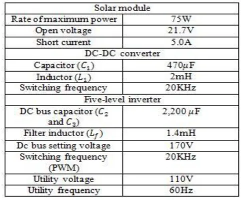
TABLE II: SIMULATION PARAMETERS
VI. SIMULATION RESULTS
To verify the performance of the photovoltaic power generation system using the five-level and nine level
inverter, MATLAB/SIMULINK is used. The main parameters of the simulations are listed in Table II. The solar
cell array consists of two strings, and each string contains eight solar modules connected in series. The capacity
1526 | P a g e Fig. 6. Simulation results for the dc–dc converter of the developed photovoltaic power generation system.
(a) Voltage ripple of dc capacitor C2 . (b) Voltage ripple of dc capacitor C3. (c) Output voltage ripple of
solar cell array. (d) Inductor current ripple of dc–dc converter.
Fig. 7. Simulation results for the dc–dc converter of the developed photovoltaic power generation system.
(a) Voltage ripple of dc capacitor C2 . (b) Voltage ripple of dc capacitor C3. (c) Output voltage ripple of
1527 | P a g e Fig. 8. Simulation results for bridge inverter of the five-level inverter. (a) Output current of the
full-bridge inverter io. (b) Input current of the full full-bridge inverter idc . (c) Driver signal of S4 . (d) Driver
signal of S5.
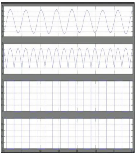
Fig. 9. Simulation results of the five-level inverter. (a) Utility voltage. (b) Output voltage of the full-bridge
1528 | P a g e The output power of the solar cell array in the developed photovoltaic power generation system is about 830 W.
Therefore, the developed photovoltaic power generation system can track the maximum power point of the solar
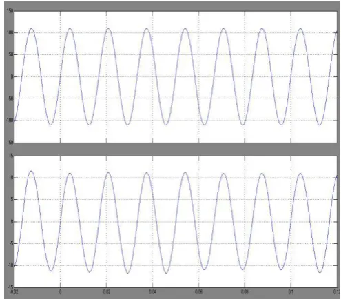
cell array effectively. Fig. 6 shows the simulation results for the five-level inverter used in the developed
photovoltaic power generation system under the steady state. The output power of the solar cell array is about
830 W. As seen in Fig. 6(b), the output current of the five-level inverter is sinusoidal and in phase with the
utility voltage. The total harmonic distortion (THD%) of the utility voltage and the output current of the
five-level inverter are 4.1% and 3.3%, respectively. As seen in Fig. 6(c) and (d),both dc capacitor voltages VC2 and
VC3 remain in balance, and their voltage is about 85 V, respectively. Therefore, the dc bus voltage is regulated
at 170 V. This verifies the nine-level inverter can perform the functions of converting solar power to ac power
with unity power factor, low THD%, and balancing two dc capacitor voltages effectively. Since dc capacitors
C2 and C3 perform the function of energy buffers, both dc capacitor voltages VC2 and VC3 contain a 120-Hz
voltage ripple. Fig. 9 shows the simulation results for the dc–dc converter of the developed photovoltaic power
generation system. Fig. 7(a) and (b) show the peak-to-peak value of the voltage ripple at dc capacitors C2 and
C3 is about 7 V. As seen in Fig. 7(c), the peak-to-peak value of the voltage ripple at the solar cell array is only
about 1.6 V. Fig. 7(d) shows the ripple of the inductor current is very small due to the use of the current mode
control. In this way, the output voltage of the solar cell array can be more stable.
Fig. 10. Simulation results of the Nine-level inverter. (a) Utility voltage. (b) Output voltage of the
full-bridge inverter. (c) Output voltage of the dual buck converter.
This verifies that the developed control method for the dc– dc converter of the developed photovoltaic power
generation system can effectively block the voltage ripple of five-level inverter delivering to the output voltage
of the solar cell array. Fig. 8 shows the simulation results for the full-bridge inverter of the five-level inverter.
1529 | P a g e current of the full-bridge inverter shown in Fig. 8(a). As seen in Fig. 8(c) and (d), the switch frequency of the
power electronic switches S4 and S5 is 60 Hz. This verifies the power electronic switches of the full-bridge
inverter are switched in low frequency, and the full-bridge inverter can convert the dc power into ac power by
commutating.
Fig. 11. Simulation results for the developed photovoltaic power generation system under the distorted
utility voltage. (a) Utility Voltage. (b) Output current of the five-level inverter.
Fig. 9 shows the simulation voltage of the five-level inverter. As seen in Fig. 9(c), the dual-buck converter
outputs a DC voltage with three levels Vdc, Vdc/2, and 0. Fig. 9(b) shows the output voltage of the dual-buck
converter is further converted to an ac voltage with five voltage levels Vdc, Vdc/2, 0, −Vdc/2,and −Vdc by the
full-bridge inverter. The voltage variation of each level is Vdc/2. This verified that the five-level inverter can
generate a five-level output ac voltage according to the utility voltage and only the power electronic switches of
the dual-buck Converter is switched in high frequency. Fig .10 shows the simulation voltages of nine level
inverter. Fig. 10(c), the dual-buck converter outputs a DC voltage with five levels. Fig. 10(b) shows the output
voltage of the dual-buck converter is further converted to an ac voltage with nine level voltages by the
full-bridge inverter. This verified that the five-level inverter can generate a nine-level output ac voltage according to
the utility voltage and only the power electronic switches of the dual-buck converter is switched in high
frequency. Fig. 11 shows the simulation results for the developed photovoltaic power generation
system under the distorted utility voltage. As seen in Fig. 11(a), the utility voltage is distorted, and its THD% is
8.4%. As seen in Fig. 11(b), the output current of the five-level inverter is still close to sinusoidal, and its
THD% is only 4.5% and the power factor is 0.99. This experiment verifies the controller of the five-level
inverter can control the output current with low THD% even when the utility voltage is distorted.
VII. CONCLUSION
A photovoltaic power generation system with a five-level and nine level inverter are developed in this paper.
The nine-level inverter can perform the functions of regulating the dc bus voltage, converting solar power to ac
1530 | P a g e detecting islanding operation. The simulation results are verify the developed photovoltaic power generation
system, and the nine-level inverter achieves the expected performance.
REFERENCES
[1.] D. Puyal, L. A. Barragan, J. Acero, J. M. Burden, and I. Millan, “AnFPGA-based digital modulator for full-
or half-bridge inverter control,”IEEE Trans. Power Electron., vol. 21, no. 5, pp. 1479–1483, Sep. 2006.
[2.] O. Lopez, F. D. Freijedo, A. G. Yepes, P. Fernandez-Comesaa, J. Malvar,R. Teodorescu, and J.
Doval-Gandoy, “Eliminating ground current in transformer less photovoltaic application,” IEEE Trans. Energy
Convers., vol.25, no. 1, pp. 140–147, Mar. 2010.
[3.] B. R. Lin and C. L. Huang, “Implementation of a Shunt-series compensator for nonlinear and voltage
sensitive load,” in Proc. IEEE Power Electron. Motion Control Conf., 2006, pp. 1–5.
[4.]U. S. Selamogullari, D. A. Torrey, and S. Salon ,A systems approach for a stand-alone residential fuel cell
power inverter design,” IEEE Trans. Energy Convers., vol. 25, no. 3, pp. 741–749, Sep. 2010.
[5.] J.Gafford,M.Mazzola, J. Robbins, and G. Molen, “A multi-kilowatt high frequency ac-link inverter for
conversion of low-voltage dc to utility power voltages,” in Proc. IEEE Power Electron. Spec. Conf., 2008,
pp. 3707– 3712.
[6.] T. H. Ai, J. F. Chen, and T. J. Liang, “A random switching method forHPWM full-bridge inverter,” IEEE
Trans. Ind. Electron., vol. 49, no. 3,pp. 595–597, Jun. 2002.
AUTHOR’S PROFILE
1. Dr. S.Siva Prasad, Professor, EEE has awarded Ph.D Electrical Engineering in
2012(February) from J. N. T. UNIVERSITY HYDERABAD and had his M.Tech with
specialization of Power Electronics in 2003.He has obtained his B.Tech Degree in
Electrical and Electronics Engineering from S V University. He is having 19 years of
Experience and currently working as Professor Vidya Jyothi Institute of Technology,
AzizNagar , Hyderabad , India . He received “Bharat Vibhushan Samman Puraskar” from “The Economic and Human Resource Development Association” in 2013 and received Young
Investigator Award in 2012. He has published about 60 technical papers in International and National Journals
and Conferences and filed one patent. He is Life member of ISTE and member of IEEE. His Research areas
include Power Electronics & Drives, PSD&FACTS Controllers
2. A.B BHAVANA REDDY presently working as assistant professor in Vidya jyothi institute of technology.
Aziz nagar gate,C.B.post, Hyderabad, Telengana.Completed B.Tech degree in electrical and electronics
engineering from Jntuh Hyderabad and then completed PG in electrical and electronics engineering as
specialization in Power electronics includes, Power electronics, HVDC, FACTS from Jntuh Hyderabad.