3523
Modified Seven Level Inverter Using Level Shifting
Pulse Width Modulation
Ms. Radhika Somakumar, Dr. J. Gayathri Monicka, Mr. Raja Pagalavan
Abstract: For achieving an output voltage waveform almost like a sinusoidal waveform the most commonly used method is by generating multi steps. In Multilevel Inverters there are three conventional topologies, of which Cascaded H-bridge type of Multilevel inverters can be treated as the most reliable topology in creating higher output voltage with less harmonics when compared to rest of them because of its modular nature. Since the requirement of separate dc sources are available naturally in these MLI, they are very much suitable for applications in solar energy. Despite the advantages MLIs have, there are some drawbacks such like the usage of huge number of switches and complex design for gate drive circuit for the respective semiconductor switches which keep on adding the problems to be addressed in mechanical and electrical design of the inverters. In this paperwork a simple topology of seven level inverter with seven switches is proposed with level shifting pulse width modulation control strategy as it provides superior performance in total harmonics distortion. For the proposed topology, MATLAB Simulation is carried out and a design has been developed for hardware. To authenticate the design and simulation a hardware implementation is also presented.
Index Terms: Multilevel Inverters, Symmetrical Inverters, Level Shifting methods, Total Harmonic Distortion.
—————————— ——————————
1
INTRODUCTION
Currently DC to AC conversion process is growing very rapidly for the area of power electronics, transmission & distribution and utilization of electric power [1]. The application of this are mostly encountered in the area of a less dv/dt, output is distortion less, good voltage & current waveform with most undesirable harmonics eliminated, less switching loss. Now depending upon the output waveform inverter classification are square wave, quasi square wave, two level PWM inverter and multilevel inverter [2]. Particularly MLI‘s has been introduced for large power and medium voltage applications. The main theoretical aspect behind the MLI structure is to get an output voltage with semiconductor switches to do the conversion process by synthesizing a staircase voltage waveform which includes several DC voltages sources. Here capacitors, batteries & renewable energy sources may be used as sources. Due to its enormous advantages in the field of electric vehicle applications and photovoltaic systems, MLIs are most frequently used compared to other inverters like voltage source and current source inverters [1],[2]. In a conventional inverter circuit, capacitor and inductor (which are large passive components) are required and as a result, the cost is increased [3],[4]. The three most frequently used types of multilevel inverters are flying capacitor, diode clamped, and H-bridge [5].
Normally we don‘t go for flying capacitor type because of a greater number of capacitors, at the same time for diode
clamped type implementation cost is too high as compared to flying capacitor types and cascaded H-bridge types [6]. As the Cascaded H-bridge multilevel inverter has the following advantages of low switching redundancy, automatic voltage sharing, low switching stresses, and requires least number of components, lower voltage of capacitors and diodes it is even more simple than diode clamped and flying capacitor [7]. The output voltage level of a Cascaded MLI is three. Henceforth a greater number of bridges are required to generate higher output voltage levels, which in turn add on the number of power semiconductor switching devices [8],[9]. So that may cause huge amount of semiconductor devices losses when the number of semiconductor switches incorporated is high. This could be got rid of by introducing multilevel inverters structure with a smaller number of switching devices [10]. Normally multilevel Inverters produces an output voltage in a stepped form consisting of input DC levels with their additive & subtractive combinations. So, the output wave form consists of several levels with both positive & negative half cycles. The part which produces level is termed as level generation & the part which produces polarity is termed as polarity generation part. Asymmetrical and symmetrical multilevel inverter structures are the two topologies which achieve the reduced switching devices number as well as maintain the output voltage level same as the conventional structures, i.e., [11]. When all the input voltage sources to a Multilevel Inverter are the same then it is termed as symmetrical source otherwise it is called as asymmetric. With these two structures, total harmonic distortion (THD) and power semiconductor devices losses can be lessened [12]. There are many techniques of modulation that are used in Symmetrical multilevel inverters, which depends on the amount or quantity of sub-modules present in the phase legs of the converters. Carrier-based PWM (CB-PWM) [13] phase-shifted PWM (PS-PWM) [14] and level-shifted PWM (LS-PWM) are the generally incorporated ones. Some other techniques are band-tolerance modulation based on hysteresis and SHE-PWM. Phase-disposition PWM (PD-PWM) is the most preferable choice of LS-PWM technique due to its better harmonic performance. Level shifted pulse width modulation is employed in this study. THD of the resultant output voltage waveform always depends upon the selection of
_____________________
Ms. Radhika Somakumar is currently pursuing Part time Ph.D degree program in electrical engineering in Anna University and works in Agni College of Technology, Thalambur Chennai. PH-7550141061. E-mail: [email protected]
Dr. J. Gayathri Monicka is currently working as professor in SRMIST,Ramapuram Chennai [email protected]
B.RajaPagalavan is currently pursuing Part time Ph.D in Anna University and working inP.T.Lee Chengalvaraya Naicker College of
Engineering and Technology
modulation techniques.
2
DESIGN
FOR
SYMMETRICAL
MULTILEVEL
INVERTER
WITH
LESSER
NUMBER
SWITCHING
DEVICES
By using a modified scheme for gating pulses generation, the design for symmetrical cascaded MLIs can be made even simple. The cascaded MLIs structure are built with bridges cascaded together. Two H bridges are used for a five-level inverter similarly when it comes to a seven-level inverter we go for three H bridges and in case of nine-level inverter the count will be four and so on. A single bridge is formed by four power semiconductor switches, so that the count of switches keeps on increasing with the voltage steps and level. Due to this the cost and switching losses for MLIs also changes accordingly. So only we have taken an initiative for reducing the cost of MLI by using a lesser count of power semiconductor switches and a simplified switching technique to provide switching pulses to the MLIs. In this paperwork, a novel method for a seven-level inverter having only seven switches has been introduced and a simplified gate pulse control circuitry is developed for the proposed topology.
3
CONTROL
STRATEGY
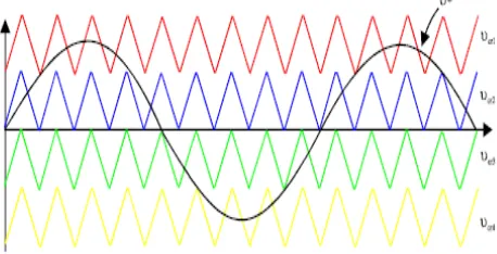
The main purpose of using modulation technique for power semiconductor devices is to create the switching signals in such a way that the output fundamental voltage waveform is merely like the sinusoidal waveform. Henceforth by attaining the output voltage waveform shape same as the sinusoidal waveform, we can bring down the lower order harmonics which in turn lessen the total harmonic distortion (THD) of the entire circuit. Based upon the switching frequencies used the MLIs are categorized as given below. Fig 1 displays the various types of modulation techniques. In this paperwork we have implemented level shifting pulse width modulation (PD) modulation technique to generate the desired output waveform.
carrier signals and the sine wave to create the required switching signals for the N level inverter. By carrying out the comparison between the carrier signals and sinusoidal waveform the switching pulses are built for the inverter. Now according to the shape of the waveforms and their patterns, they are divided as: 1) Phase Shifting PWM; 2) Level shifting PWM. In PS-PWM techniques the frequency and amplitude of carrier signals are same but there is a phase change among them. When it comes to LS-PWM, only difference in the levels of biasing happens and the above explained three parameters remain the same.
3.1 Level Shifted Carrier Pulse Width Modulation
For each carrier wave the time values for carriers‘ signals are entered as [0 1/600 1/300] and at the same time the values of output are marked accordingly with the carrier waves disposition. After a comparison is done, the output signals of comparator are transferred to the IGBT switches. This technique is branched into 3 types:
3.1.1 Phase Opposition Disposition (POD)
In this classification of level shift PWM technique the phase difference that exist between the modulating signal above the reference (zero) line and the modulating carrier signals below
the reference line is 180
degrees.
fig 2: Waveform for Phase Opposition Disposition
3.1.2 Phase Disposition (PD)
3525 modulating carrier and nearby carriers is 180.
fig 4: Waveform for Alternative Phase Opposition
Disposition
In the work proposed here, phase disposition PWM method has been implemented. In common, the comparison is done between sinusoidal reference signal and the triangular carrier signals to transmit the switching signals to circuit. In carrier based PWM implementation, during each time period the modulation signal is compared with the carrier signals and depending on which one is having high value, switching pulses are produced (Fig 6).
4
MATLAB
MODELLING
AND
EXPERIMENTAL
SETUP
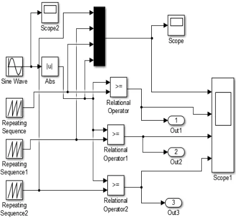
The components used for the proposed work includes four MOSFETS which form the H-bridge like a single-phase voltage source inverter which generates positive as well as negative voltages. In the input side, three batteries of 12 volt each are used, together with which two diodes and three MOSFETS are used to build voltage levels of V,2V and 3V. MATLAB Simulink Diagram is given in Fig 5. The pulse generator blocks are used to supply gate pulses to the MOSFETS, and it is set up through gates as illustrated in the Fig 6. The results of MATLAB simulation and value of THD is shown in Fig 7 and Fig 8 respectively.
fig 5: Simulink Diagram for the proposed Seven Level
Asymmetric Multilevel Inverter.
fig 7: Output Voltage Waveform
fig 8: Total Harmonic Distortion
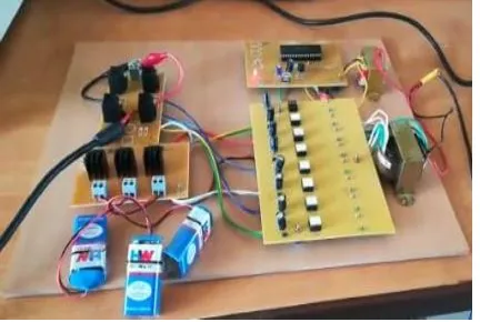
The hardware setup developed for the proposed converter is shown in Figure 9. It is incorporated by a PIC micro-controller. The software system like Proteus, MP lab, and Micropro are being used for the need of system design and coding the pulses to the PIC controller. The power supply circuit is outlined in such a way that it will have a control over the PIC and driver circuit to transmit the gate pulses to the MOSFET. The output voltage that is displayed in CRO is shown in Figure 10.
fig10: Seven level Output Waveform
5
CONCLUSION
A modified seven level inverter topology is used which is having superior features when compared with conventional topologies over the parameters such as the number of power switches required, individual dc supplies, control strategy, reliability and cost. The proposed topology is considered and used efficiently for the various applications of converters like HVDC, FACTS, Photovoltaic systems, UPS etc. The Hardware set up and experimental results of the proposed seven-level inverter is included. From the simulation results it is evident that the proposed inverter can be used efficiently as it incorporates lesser count of components which makes the circuit become less complex and the Total Harmonic Distortion is reduced (THD) to 7.26 %.
REFERENCES
[1]K.K.Gupta, Alekh Ranjan, Pallavee Bhatnagar and Shailendra Jain ―Multilevel Inverter with reduced device count-A review‖ in IEEE Trans. on Power electronics, 2015
[2]J.Rodriguez,L.G. Franquelo, S.KOuro, J.I. Leon, R.C.Portillo,M.A. Perez ―Multilevel converters-An enabling technology for high power application‖, in proceedings of IEEE, vol.97, no.11, pp.1786-1817,Nov.2009.
[3]O. L. Jimenez, et al., ―THD in cascade multilevel inverter symmetric and asymmetric,‖ Proc. - 2011 IEEE Electron. Robot. Automot. Mech. Conf. CERMA 2011, pp. 289-295, 2011. [4]Grain P. Adam (Aug 2008), Capacitor Balance Issues of the
Diode-Clamped Multilevel Inverter Operated in a Quasi Two State Mode, IEEE Transaction on Industrial Electronics volume.55 no:08 pp-3088-3099.
3527 [9]Roshankumar, P., Rajeevan, P.P., Mathew, K., Gopakumar, K.,
Leon, J.I. and Franquelo, L.G. (2012) A Five-Level Inverter Topology with Single-DC Supply by Cascading a Flying Capacitor Inverter and an H-Bridge. IEEE Transactions on Power Electronics, 27, 3505.
[10]K. K. Gupta, A. Ranjan, P. Bhatnagar, L. K. Sahu, and S. Jain, Multilevel Inverter Topologies with Reduced Device Count: A Review, IEEE Trans. Power Electron., vol. 31, no.1, pp.135-151, Jan 2016.
[11]Gayathri Monicka J., Jamuna V., Hemalatha K. (2015) A New Approach for Torque Ripple Minimization of PMBLDC Motor Drive. In: Kamalakannan C., Suresh L., Dash S., Panigrahi B. (eds) Power Electronics and Renewable Energy Systems. Lecture Notes in Electrical Engineering, vol 326. Springer, New Delhi.
[12]Gayathri Monicka, J.& V.Jamuna ―Optimal Switching Strategy of Level shifted carrier based PWM technique for Asymmetric Multilevel Inverter‖ International Journal of Engineering Science (ISSN: 0020-7225) ELSEVIER, vol.113
[13]Gayathri Monicka, J, Jamuna, V 2015, ‗Control of ternary voltage progression based cascaded multilevel inverter using classy split multicarrier pulse width modulation‘, Turkish Journal of Electrical Engineering and Computer Sciences.