http://www.sciencepublishinggroup.com/j/optics doi: 10.11648/j.optics.20180702.12
ISSN: 2328-7780 (Print); ISSN: 2328-7810 (Online)
Structural and Optical Properties of ZnO Thin Films
Deposited by Pyrolysis Spray Method: Effect of Substrate
Temperature
Abdelkader Hafdallah
1, *, Fahima Djefaflia
2, 3, Narimane Saidane
31Applied and Theoretical Physics Laboratory, Department of Material Sciences, University Larbi Tebessi, Tebessa, Algeria 2
Department of Physics, Badji Mokhtar University, Annaba, Algeria
3
Faculty of Sciences, University of Souk-Ahras, Souk-Ahras, Algeria
Email address:
*
Corresponding author
To cite this article:
Abdelkader Hafdallah, Fahima Djefaflia, Narimane Saidane. Structural and Optical Properties of ZnO Thin Films Deposited by Pyrolysis Spray Method: Effect of Substrate Temperature. Optics. Vol. 7, No. 2, 2018, pp. 68-73. doi: 10.11648/j.optics.20180702.12
Received: June 18, 2018; Accepted: July 23, 2018; Published: September 26, 2018
Abstract:
During the last decades, thin films of ZnO have given rise to a great interest, as transparent conducting oxides. This is due the optical and electrical properties of zinc oxide; it’s very high thermal and chemical stability, its non-toxicity as well as his abandonment in nature. The transparent conducting ZnO thin films were deposited on glass substrate by pyrolysis spray technique. Zinc acetate was used as starting solution with a molarity of 0.1 M. The structural and optical properties of the ZnO thin films were studied as a function of the substrate temperatures in the range of 100 to 400°C. Structural properties have been studied by X-ray diffraction (XRD) technique. The preferred orientation for ZnO thin films lies along (002) direction. From XRD data, the average crystallite size is determined from scherrer formula. The grain size is in the range of 10~27. The transmittance of the films is enhanced from 60 to 85% in the visible region in the range from 400 to 1100 nm by increasing the substrate temperature. The optical band gap energy attenuates from 3.67 to 3.25eV and whereas the Urbach energies of the films increase from 226 to 91.2 meV with increasing the substrate temperature from 100°C to 400°C.Keywords:
ZnO, Thin Films, Substrate Temperature, Pyrolysis Spray, XRD, Transmission1. Introduction
ZnO is one of the most important semiconductor materials due to its wide band gap (3.37 eV) at room temperature and large exciton binding energy (60 meV) at room temperature [1]. Transparent conducting oxides (TCO) are widely used in microelectronic devices, light emitting diodes, thin film, antireflection coatings for transparent electrodes in solar cells, gas sensors in surface acoustic [2–5]. ZnO was found various technological applications such as solar cells [1, 2], active material for highly sensitive humidity and oxygen gas sensors [3], transparent electrodes for flat –panel displays [4], p-n junction diodes, UV photo detectors [5] and ultraviolet light emitting diodes [6]. To improve ZnO properties, various growth techniques, including chemical vapor deposition [8], sol–gel method [9], electrochemical deposition [7], sputter
deposition [8], hydrothermal technique [9] and spray pyrolysis technique (SPT) [10] have been employed to obtain pure ZnO thin films on various substrates. Spray pyrolysis is a versatile technique for deposition of metal oxides because of its cheapness and easy process control which gives the possibility of obtaining films with the required properties for different applications
2. Experimental Details
The number of thin films of pure ZnO was synthesized by spray pyrolysis method. Zinc acetate dihydrate Zn(CH3COO)2. 2H2O with methanolwas used as precursor
solution.
In order to get the 0.1M homogenous transparent solution of Zn(CH3COO)2. 2H2O, the 2.195 g of Zinc acetate
dihydrate was dissolved in 20 ml methanol and stirred at room temperature. The thin films were deposited on well cleaned microscopic glass (1.25x 1.5 cm2) substrates using a commercial nebulizer by spraying the above transparent
precursor solution on preheated glass substrate at different substrate temperature (100, 200, 300, 400 ) using a resistive heating set-up (The samples used in this study were deposited using a device made in the laboratory). These precursors were sprayed onto glass substrates placed below a substrate holder heated to a fixed temperature 350°C.
Our interest is to study the effect of substrate temperature on the optical and structural properties of these films. For this we used X-ray diffraction for structural characterizations and UV-Visible optical transmission spectroscopy for the optical characterization of our films.
Table 1. The experimental conditions for the deposited ZnO thin films.
Deposition time(min) Distance nozzle-substrate(cm) Solution concentration (M) Substrate temperature(°C)
Zinc acetate C4H6O4Zn.2H2O 5 25 0.1 100, 200, 300 and 400
3. Results and Discussion
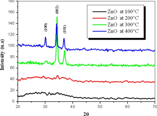
Figure 1 shows XRD patterns of ZnO thin films as a function of substrate temperature. The samples are polycrystalline in nature which shows hexagonal crystal structure (JCPDS card no. - 01-075-1526) and it prefers the orientation along (002) plane [12]. The observed minor planes include (100) and (101). The optimum substrate temperature for the deposition of crystallized ZnO thin films is 400°C. At this temperature, atoms have optimum energy for chemical reaction and arrange along the preferred orientation of (002) [12]. The highest intensity of lattice plane (002) is assigned to the crystal growth with preferential
orientation along c-axis. Except in the case of substrate temperature 100°C note the amorphous spectrum because of insufficient temperature to manufacture a thin film of ZnO.
The increasing substrate temperature generally improves the crystalline structure of thin films. Film characterization using Fourier Transform Infrared Spectroscopy (FTIR), photoluminescence spectroscopy (PL), and ultraviolet– visible (UV–Vis) optical transmission spectroscopy suggests the onset of ZnO growth at temperatures as low as 100°C as well as the transformation to a polycrystalline phase at deposition temperatures > 200°C reported by Adamopoulos et al [13].
Figure 1. XRD patterns of ZnO thin films deposited at different substrate temperature.
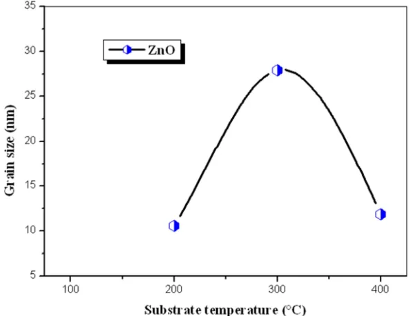
The grain size is simply determined using the Scherrer formula [14-15]:
D= 0.9λ/βcosӨ
Figure 2 shows the variation of the size of the grains as a function of substrate temperature, according to the X-ray spectrum observation. Note that the case of ZnO deposited at (100°C) is an amorphous spectrum therefore it is not grain size it is by a crystallographic structure, the grain size varies
between 200°C and 400°C, note an increase between 200°C and300°C this increase due to the improvements of the crystallinity, then a decrease between 300°C and 400°C this decrease due to the emergence of the other peak (001) and (101) [17].
Figure 2. Variation of grain size with substrate temperature.
In figure3, the transmission spectra in the range 300 to 1100 nm are grouped together with ZnO films. Although the general look of the spectra is identical, these are composed of two regions:
1. A region of high transparency located between 400 and 1100 nm, the value of the transmission is of the order of 60 to 85%. This value, reported by several authors [16], confers on the thin films of ZnO, deposited with different substrate temperatures, the transparency character in the visible. This confirms that the optimal
deposition temperatures for obtaining transparent, uniform and stoichiometric ZnO films are in the vicinity of 300°C. Note that the choice of this optimum substrate temperature is based on previous work done within our team
2. A region of high absorption. This region corresponds to the fundamental absorption (λ<400nm) in ZnO films. This absorption is due to the inter-band electronic transition. The variation of the transmission in this region is exploited for the determination of the gap.
It can be seen that from a spectrum of transmission in the visible, we can quickly determine the thickness of the material and the optical gap.
For a direct gap such as that of the ZnO, α is expressed as a function of gap (Eg) according to the equation next [14]:
(αhυ) = A(hυ – Eg)1/2
Where
A: Constant Eg (eV):
hυ: photon energy
Figure 4 shows the width of the band gap (optical gap) can be determined from the extrapolation of the linear part of the curve representing the function (αhυ)2=f(hυ) ( direct gap) and of its intersection with abscissa axis ( photon energy axis)
Figure 4. Typical variation of (αhυ)2 as a function of photon energy (hυ).
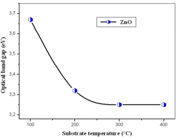
The transmission drop for wavelengths below 400 nm corresponds to the absorption in ZnO due to the transition between the valence band and the conduction band, this region is used to determine the energy of the optical gap. We reported the variation of the optical gap of ZnO films in figure 5. As can be seen, in this figure note a total decrease in optical gap between (100°C and 400°C) this decrease
interpreted by:
- In the case where ZnO deposited at (100°C) the X-ray spectrum confirms that the amorphous layer does not have a good crystallite ZnO (3.67eV).
-From a substrate temperature of 200°C, slight decreases is observed in optical gap values and are very logical with the literature [18].
Figure 5. Variation of optical band gap with substrate temperature.
1,0 1,5 2,0 2,5 3,0 3,5 4,0 4,5
0,00E+000 2,00E+010 4,00E+010 6,00E+010 8,00E+010
ZnO 400°C Eg=3.25 eV
(
αααα
h
υυυυ
)
2
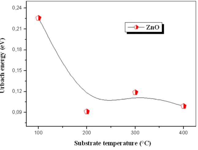
Another important parameter that characterizes the disorder of the material is the tail energy Urbach. According to Urbach's law the expression of the coefficient absorption is of the form:
α= α0 exp(hυ/E00)
Where
E00: Urbach energy
Figure 6 shows the variation of urbach energy (disorder) of the ZnO films as a function of substrate temperature. From this figure, we see that the temperature affects the
organization of the deposited thin films. Indeed, the substrate temperature influences the mobility of the atoms arriving at the surface during film growth. At high substrate temperature, the atoms arriving at the surface have enough energy to move and find a favorable site. A decrease in urbach energy between (100°C and 400°C) was observed with the substrate temperature. This decrease is interpreted by the increase of the temperature of the substrate because the increase of the substrate temperature due to the network relaxation [16-17].
Figure 6. Variation of Urbach energy with substrate temperature.
4. Conclusion
In the present investigation, chemical spray deposition technique (SPT) was used to grow undoped ZnO thin films on glass substrates by varying the substrate temperature. The influence substrate temperature on the structural and optical properties investigated here was found to be significant. The XRD results show the presence of the ZnO wurtzite phase with preferential orientation (002) of the film growth along the c-axis, concerning the deposited layer at 100°C, which presents a phase totally amorphous. The average crystalline size increases with increase in substrate temperature indicating better crystallinity of films deposited at higher substrate temperature (300°C) as the films become more uniform and dense, grain size is varied with substrate temperature from 10 to 28 nm. The optical transmittance of polycrystalline films was varied from 60% to 85% in the visible region. The obtained optical gap values for the different substrate temperature are in good agreement with the data of literature (3.67-3.25eV).
References
[1] Laxmi Dangol and Leela Pradhan Joshi, Journal of Institute of Science and Technology, 21 (2016) 61–64.
[2] A. Zaier, A. Meftah, A. Y. Jaber, A. A. Abdelaziz, M. S. Aida, Journal of King Saud University–Science, 27 (2015), 356-360.
[3] M. Lalanne, J. M. Soon, A. Barnabe, L. Presmanes, I. Pasquet and Ph. Tailhades, Journal of Materials Research, 25(2010) 2407-2414.
[4] A. Hafdallah, K. Derrar, M. S. Aida et N. Attaf, Afrique Science, 12 (2016) 26-33.
[5] H. Belkhalfa, H. Ayed, A. Hafdallah, M. S. Aida, R. TalaIghil, Optik, (2016), 127, 2336–2340.
[6] U. E. Uno, K. U. Isah, & T. O. Daniel, Global Journal of Engineering, Design & Technology, (2015) Vol. 4 (1), 1-7.
[8] Yacine Aoun, Boubaker Benhaoua, Brahim Gasmi, and Said Benramache, Journal of Semiconductors, 36 (2015)1-5.
[9] Hassan ZareAsl, Seyed Mohammad Rozati, Materials Research. (2018); 21(2): 20170754.
[10] Yasmeen Z. Dawood, Salah QaduriHaza, SabaJameelHasan, Najiba Abdullah Hasan, Journal of Applied Physics, 7 (2015) 50-54.
[11] Rajesh Biswal, Luis Castañeda, Rosario Moctezuma, Jaime Vega-Pérez, María De La Luz Olvera and Arturo Maldonado, Materials, 5 (2012) 432-442.
[12] Vinoth Kumar Jayaraman, Yasuhiro Matsumoto Kuwabar, Arturo Maldonado Álvarez, María de la luz Olvera Amador, Materials Letters 169 (2016) 1–4.
[13] George Adamopoulos, Aneeqa Bashir, William P. Gillin, StamatisGeorgakopoulos, Maxim Shkunov, Mohamed A. Baklar, Natalie Stingelin, Donal D. C. Bradley and Thomas D. Anthopoulos, Advanced Functional Materials, Volume 21, Issue 3, pages 525–531, February 8, 2011.
[14] A. Hafdallah, F. Yanineb, M. S. Aida and N. Attaf, J. Alloys. Compd, 509(26) (2011) 7267–7270.
[15] Abdelkader Hafdallah, Abderrahman Azzedine, Hanane Belhani, Mohamed Salah Aida, Nadhir Attaf, American Journal of Nano Research and Applications, (2017), 5, 87–90.
[16] F. Ynineb, A. Hafdallah, M. S. Aida, N. Attaf, J. Bougdira, H. Rinnert, S. Rahmane, Mater. Sci. Semicond. Process, 16 (2013), 2021-2027.
[17] A. Hafdallah, A. Ferdi, M. S. Aida, N. Attaf and A. Amara, International Journal of Advanced Research, 3 (2015) 240– 246.