An FPGA-Based Parallel Distributed Arithmetic Implementation
of the 1-D Discrete Wavelet Transform
Ali M. Al-Haj
Department of Computer Engineering, Princess Sumaya University for Technology, Al-Jubeiha P.O.Box 1438, Amman 11941, Jordan
Keywords: discrete wavelet transform, parallel distributed arithmetic, parallel implementation, Virtex FPGAs. Received: February 7, 2004
The fine grained parallelism inherent in Field Programmable Gate Arrays (FPGAs) may be well exploited to implement the computation-intensive discrete wavelet transform, which is increasingly employed in multimedia consumer electronics. In this paper, we describe a parallel implementation of the discrete wavelet transform and its inverse using Virtex FPGAs. We make maximal utilization of the look-up table architecture of the Virtex FPGAs by reformulating the wavelet computation in accordance with the parallel distributed arithmetic algorithm. The reported single chip implementation may be used effectively in the construction of low-power, wavelet-based MPEG-4 and JPEG2000 decoders.
Povzetek: Opisana je implementacija FPGA algoritma za uporabo v uporabniški elektroniki.
1
Introduction
Digital signal processing algorithms are increasingly employed in modern wireless communications and multimedia consumer electronics, such as cellular telephones and digital cameras. Traditionally, such algorithms are implemented using programmable DSP chips for low-rate applications [1], or VLSI application specific integrated circuits (ASICs) for higher rates [2]. However, advancements in Filed Programmable Gate Arrays (FPGAs) provide a new vital option for the efficient implementation of DSP algorithms [3]. FPGAs are bit-programmable computing devices which offer ample quantities of logic and register resources that can easily be adapted to support the fine-grained parallelism of many pipelined digital signal processing algorithms [4] - [6].
At the heart of most digital signal processing algorithms is a multiply-and-accumulate function that can be implemented more efficiently with distributed arithmetic architectures [7]. These architectures make extensive use of look-up tables, which make them ideal for implementing digital signal processing functions on Xilinx FPGAs, whose architectures are based on look-up tables. Moreover, distributed architectures are suitable for low power portable applications, because they replace the costly multipliers with shifts and look-up tables [8].
An emerging arithmetic-intensive digital signal processing algorithm is the discrete wavelet transform [9] . The perfect reconstruction and lack of blocking artifacts properties of this transform have proven to be extremely useful for image and video coding applications [10]. Furthermore, the basis functions of the discrete
wavelet transform match the human visual profiles, and hence provide subjectivity pleasing images at high compression rates. By virtue of such attractive features of the wavelet transform, it has been adopted by the recent multimedia compression standards MPEG-4 [11] and JPEG2000 [12].
In this paper, we describe a parallel and high speed, single-chip implementation of the discrete wavelet transform and its inverse using Virtex FPGAs [13]. We make maximal utilization of the look-up table architecture of Virtex FPGAs by reformulating the wavelet transform computation in accordance with the parallel distributed arithmetic algorithm. Unlike most papers in literature which report on single-chip VLSI architectures of the forward discrete wavelet transform only [14] - [17], this paper describes an actual implementation of both the forward and inverse transforms. Therefore, the implementation may be used in the construction of effective MPEG-4 and JPEG2000 decoders.
Finally, the paper is organized as follows. Section two gives preliminaries of the implementation which includes an overview of the discrete wavelet transform and Xilinx Virtex FPGAs. Section three describes principles of parallel distributed arithmetic, and section four describes our parallel implementation which is based on parallel distributed arithmetic. Performance results are presented in section five, and discussed in section six. Finally, some concluding remarks are presented in section seven.
2
Preliminaries
compute the coefficients of the discrete wavelet transform. We also give an overview of Xilinx Virtex FPGAs which are used as our single-chip implementation platform.
2.1
Discrete Wavelet Transform
Coefficients
Wavelets are special functions which, in a form analogous to sines and cosines in Fourier analysis, are used as basal functions for representing signals. The coefficients of the discrete wavelet transform can be calculated recursively and in a straight forward manner using the well-known Mallat’s pyramid algorithm [18]. Based on Mallat’s algorithm, the discrete wavelet coefficients of any stage can be computed from the coefficients of the previous stage using the following
iterative equations:
)
1
(
)...
2
(
)
1
,
(
)
,
(
n
j
W
m
j
h
0m
n
W
m L
L
=
∑
−
−
)
2
)...(
2
(
)
1
,
(
)
,
(
n
j
W
m
j
h
1m
n
W
m L
H
=
∑
−
−
Where WL(n,j) is the nth scaling coefficient at the jth
stage, WH(n,j) is the nth wavelet coefficient at the jth
stage, and h0(n) and h1(n) are the dilation coefficients
corresponding to the scaling and wavelet functions, respectively. In order to reconstruct the original data, the DWT coefficients are upsampled and passed through another set of low pass and high pass filters, which is expressed as
)
3
(
...
...
)...
2
(
)
1
,
(
)
2
(
)
1
,
(
)
,
(
1 0l
n
g
j
l
W
k
n
g
j
k
W
j
n
W
l H k L L−
+
+
−
+
=
∑
∑
where g0(n) and g1(n) are respectively the
low-pass and high-low-pass synthesis filters corresponding to the mother wavelet. It is observed from Equation (3) that the
jth level coefficients can be obtained from the (j+1)th
level coefficients.
Daubechies 8-tap wavelet has been chosen for this implementation. This wavelet type is known for its excellent special and spectral localities which are useful properties in image compression [19]. The filters coefficients corresponding to this wavelet type are shown in Table 1. H0 and H1 are the input
decomposition filters and G0 and G1 are the output
reconstruction filters.
Table 1. Daubechies 8-tap wavelet filter coefficients.
H0 H1 G0 G1
-0.0106 0.2304 -0.2304 -0.0106 -0.0329 0.7148 0.7148 0.0329 0.0308 0.6309 -0.6309 0.0308
0.1870 -0.0280 -0.0280 -0.187 -0.0280 -0.1870 0.1870 -0.0280 -0.6309 0.0308 0.0329 0.6309 0.7148 0.0329 -0.0329 0.7148 -0.2304 -0.0106 -0.0106 0.2304
2.2
Virtex FPGAs: Architecture and
Programming
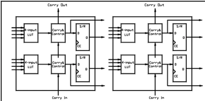
One of most advanced FPGA families in industry is the FPGA series produced by Xilinx [20]. The Virtex user-programmable gate array comprises two major configurable elements: configurable logic blocks (CLBs) and input/output blocks (IOBs). Each CLB is composed of two slices as shown in Figure 1. A slice contains 4-input, 1-output LUTs and two registers. Interconnections between these elements are configured by multiplexers controlled by SRAM cells programmed by a user’s bitstream. The LUTs allow any function of five inputs, and two functions of four inputs, or some functions of up to nine inputs to be created within a CLB slice. This structure allows a very powerful method of implementing arbitrary, complex digital logic.
Fig. 1. Simplified Architecture of Virtex configurable logic block.
Virtex FPGAs are programmed using Verilog HDL; a popular hardware description language [21]. The language has capabilities to describe the behavioral nature of a design, the data flow of a design, a design’s structural composition, delays and a waveform generation mechanism. Models written in this language can be verified using a Verilog simulator. As a programming and development environment, Xilinx ISE Foundation Series tools have been used to produce a physical implementation for the Viretx FPGA.
3
Distributed Arithmetic
)
4
...(
...
...
...
2
)
(
2
1 1 1 0 1 1 1F
F
x
a
a
x
Y
j B j j N i i i j B j N i i ij−
=
−
+
⎥
⎦
⎤
⎢
⎣
⎡
=
− − = = − − = =∑
∑
∑ ∑
Where the input data words xi have been represented by
the 2’s complement number presentation in order to bound number growth under multiplication. The variable
xij is the jthbit of the xi word which is Boolean, B is the
number of bits of each input data word and x0i is the sign
bit. Distributed arithmetic is based on the observation that the function Fjcan only take 2N different values that
can be pre-computed offline and stored in a look-up table. Bit j of each data xij is then used to address this
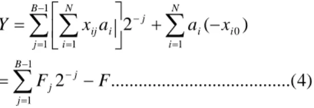
look-up table. Equation (4) clearly shows that the only three different operations required for calculating the inner product. First, a look-up to obtain the value of Fj,
then addition or subtraction, and finally a division by two that can be realized by a shift.
3.1
Parallel Realization
In its most obvious and direct form, distributed arithmetic computations are bit-serial in nature, i.e., each bit of the input samples must be indexed in turn before a new output sample becomes available. When the input samples are represented with B bits of precision, B clock cycles are required to complete an inner-product calculation. A parallel realization of distributed arithmetic corresponds to allowing multiple bits to be processed in one clock cycle by duplicating the LUT and adder tree. In a 2-bit at a time parallel implementation, the odd bits are fed to one LUT and adder tree, while the even bits are simultaneously fed to an identical tree. The bits partials are left shifted to properly weight the result and added to the even partials before accumulating the aggregate. In the extreme case, all input bits can be computed in parallel and then combined in a shifting adder tree.
3.2
Virtex Implementation
The Xilinx Virtex slices have the ability to implement distributed memory instead of logic. Each 4-input LUT in a slice may be used to implement a 16x1 ROM or RAM, or the two LUTs may be combined together to create a 32x1 ROM or RAM or a 16x1 dual-port RAM. This allows each slice to trade logic resources for memory in order to maximize the resources available for a particular application. Distributed Arithmetic for inner product generation can be easily implemented in the LUT-based Xilinx Virtex FPGAs. The inner product production basically consists of table-lookup operations and additions. Thus RAM or ROM can be employed holding table values, and table lookup operations can be performed, and then a parallel adder usually follows to sum up LUT values provided by ROM or RAMs.
4
Parallel DA Implementation
The discrete wavelet transform equations can be efficiently computed using the pyramid filter bank tree shown in Figure 2. In this section we describe a parallel distributed arithmetic implementation of the filter banks shown. We start by deriving a parallel distributed arithmetic structure of a single FIR filter. We then describe the implementation of the decimator and interpolator; the basic building blocks of the forward and discrete wavelet transforms, respectively.
X[n]
1
H (z)
2 H (z)0
2
H (z)1
H (z)0 2 2
H (z)1
H (z)0 2
2 H [n]1
2 G (z)
2 G (z)0 1 Y[n] 0 G (z) 2 G (z) 2 1 2 2
G (z)0 G (z)1
H [n]2
H [n]3
L [n]3
L [n]3
H [n] H [n]3 2
H [n]1
( a )
( b )
Fig. 2. Mallat's quadratic mirror filter tree used to compute the coefficients of the (a). forward and (b). inverse wavelet transforms.
4.1
Parallel DA FIR Filter Structure
All filters in the pyramid tree structure shown in Figure 2 are constructed using FIR filters because of their inherent stability. Most discrete wavelet transform implementations reported in literature employ the direct FIR structure, in which each filter tap consists of a delay element, an adder, and a multiplier [23] . However, a major drawback of this implementation is that filter throughput is inversely proportional to the number of filter taps. That is, as filter length is increased, the filter throughput is proportionately decreased. In contrast, throughput of an FIR filter constructed using distributed arithmetic is maintained regardless of the length of the filter. This feature is particularly attractive for flexible implementations of different wavelet types since each type has a different set of filer coefficients.
Fig. 3. A DA implementation of the Daubechies FIR filter.
Since the LUT size in a distributed arithmetic implementation increases exponentially with the number of coefficients, the LUT access time can be a bottleneck for the speed of the whole system when the LUT size becomes large. Hence we decomposed the 8-bit LUT shown in Figure 3 into two 4-bit LUTs, and added their outputs using a two-input accumulator. The 4-bit LUT partitioning is optimum in terms of logic resources utilization, since this matches naturally the Virtex slice architecture, shown in Figure 1, which uses 4-input LUTs. The modified partitioned-LUT architecture is shown in Figure 4. The total size of storage is now reduced since the accumulator occupies less logic resources than the larger 8-bit LUT. Furthermore, partitioning the larger LUT into two smaller LUTs accessed in parallel reduces access time.
Fig. 4. A partitioned-LUT DA implementation of the Daubechies FIR filter.
A parallel implementation of the inherently serial distributed arithmetic (SDA) FIR filter, shown in Figure 4, corresponds to partitioning the input sample into M
sub-samples and processing these sub-samples in parallel. Such a parallel implementation requires
M-times as many memory look-up tables and so comes at a cost of increased logic requirements. We describe below the implementation of our PDA FIR filter at two different degrees of parallelism; a 2-bit PDA FIR filter and a fully parallel 8-bit PDA FIR filter.
A 2-bit parallel distributed arithmetic (PDA) FIR filter implementation is shown in Figure 5. It corresponds
to feeding the odd bits of the input sample to an SDA LUT adder tree, while feeding the even bits, simultaneously, to an identical tree. Compared to the serial DA filter, shown is Figure 4, the shift registers are each replaced with two similar shift registers at half the bit size. The odd bit partials are left shifted to properly weight the result and added to the even partials before accumulating the aggregate by a 1-bit scaling adder. Finally, since two bits are taken at a time, the scaling accumulator is changed from 1-to-2-bit shift (1/4) for scaling.
Fig. 5. A 2-bit PDA Daubechies FIR filter.
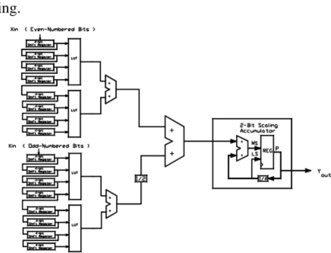
As for the fully parallel 8-bit PDA FIR filter implementation, the 8-bit input sample is partitioned into eight 1-bit sub-samples so as to achieve maximum speed. Figure 6 shows the ultimate fully parallel PDA FIR filter, where all 8 input bits are computed in parallel and then summed by a binary-tree like adder network. The lower input to each adder is scaled down by a factor of 2. No scaling accumulator is needed in this case, since the output from the adder tree is the entire sum of products.
Fig. 6. (a). A single-bit and (b). an 8 -bit PDA Daubechies FIR filter.
4.2
Decimator Implementation
Down sampling an input sequence x[n] by 2 generates an output sequence y[n] according to the relation y[n] =
x[2n]. All input samples with indices equal to an integer
multiple of 2 are retained at the output, and all other samples are discarded. Therefore, the sequence y[n] has a sampling rate equal to half of the sampling rate of
x[n].
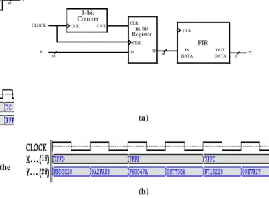
We implemented the decimator as shown in Figure 7a. The input data port of the PDA FIR filter is connected to the external input samples source, and its clock input is tied with the clock input of a 1-bit counter. Furthermore, the output data port of the PDA FIR filter is connected to the input port of a parallel-load register. The register receives or blocks data appearing on its input port depending on the status of the 1-bit counter. Assuming an unsigned 8-bit input sample is used, the decimator operates in such a way that when the counter is in the 1 state, the PDA FIR data is stored in the parallel load register, and when the counter turns to the 0 state, the PDA FIR data is discarded.
The decimator operation was modeled and verified using Verilog’s functional simulator. The corresponding simulation waveform is displayed in Figure 7b. As shown, a random input sample X enters the decimator at a rate of 1sample/1 clocks , and an output filtered sample Y leaves the decimator at a rate of 1sample/ 2clocks. The input frequency is clearly halved by the decimator. We maintained sufficient precision of the decimator output sample as indicated by number of bits in the parenthesis. Allocating sufficient bits to the intermediate and output coefficients has been a necessary step to keep the perfect reconstruction capabilities of the discrete wavelet transform.
FIR
DATA IN CLK
DATA OUT CLK
Counter1-bit
OUT
m-bit Register
Q D
CLK CLOCK
X
n m m Y
(a)
(b)
Fig. 7. (a). Implementation and (b). functional simulation of the decimator.
4.3
Interpolator implementation
Wavelets are The basic building block of the inverse discrete wavelet transform filter bank is the interpolator which consists of a parallel DA, anti-imaging FIR filter, proceeded by an sampling operator [24]. In up-sampling by a factor of 2, an equidistant zero-valued sample is inserted between every two consecutive samples on the input sequence x[n] to develop an output sequence y[n], such that y[n] = x[n/2] for even indices of n, and 0 otherwise. The sampling rate of the output sequence y[n] is twice as large as the sampling rate of the original sequence x[n].
We implemented the interpolator as shown in Figure 8a. The input data port of the PDA FIR filter is connected to the output port of a parallel-load register. Furthermore, the input port of the register is connected to the external input sample source, and its CLK input is tied with the CLK input of a 1-bit counter. The operation of the register depends on the signal received on its active-high CLR (clear) input from the 1-bit counter. Assuming the input signal source sends out successive samples separated by 2 clock periods, the interpolating filter operates in such a way that when the counter is in the 0 state, the register passes the input sample X to the PDA FIR filter, and when the counter turns to the 1 state, the register is cleared, thus transferring a zero to the PDA FIR filter. That is, a zero is inserted between every tow successive input samples.
The interpolator operation was modeled and verified using Verilog’s functional simulator. The simulation waveform is displayed in Figures 8b. The filter receives an input sample X at the rate of 1 sample/2 clocks , and sends out its filtered sample Y at the rate of 1 sample/1 clock. The input frequency is clearly doubled by the interpolator. Also, similar to the decimator, we maintained sufficient precision of the interpolator output as indicated by number of bits in the parenthesi
1-bit Counter
CLOCK
X m
CLK
m OUT
D CLR
CLK Q
n Y DATA
IN CLK
FIR
DATA OUT
Registerm-bit
(a)
(b)
5
Implementation Results
We have implemented the PDA filter bank architectures described in the previous section using one of the largest available Xilinx Virtex FPGA devices, XCV300. This device contains 322,970 gates ( 3072slices) and can operate at a maximum clock speed of 200 MHz. Therefore, performance is usually measured with respect to two evaluation metrics; the throughput (sample rate) and is given in terms of the clock speed, and device utilization, and is given in terms number of Virtex logic slices used by the implementation.
In the 2-bit PDA FIR implementation, the forward discrete wavelet transform operated at a throughput of 48.1 MHz, and required 645 Virtex slices which represents around 21 % of the total 3072 slices. Throughout of the inverse discrete wavelet transform was 46.5 MHz, and the hardware requirement was 707 slices which represent around 23 % of the total Virtex slices. On the other hand, the fully 8-bit PDA implementation, and as expected, performed much better. The forward discrete wavelet transform operated at a throughput of 154.6 MHz, and required 1167 Virtex slices which represents around 38 % of the total 3072 slices. Throughout of the inverse discrete wavelet transform was 151 MHz, and the hardware requirement was 1352 slices which represent around 44 % of the total Virtex slices.
The bit stream corresponding to the 8-bit PDA implementation was downloaded to a prototyping board called the XSV-300 FPGA Board, developed by XESS Inc [25]. The board is based on a single Xilinx XCV300 FPGA. It can accept video with up to 9-bits of resolution and output video images through a 110 MHz, 24-bit RAMDAC. Two independent banks of 512K x 16 SRAM are provided for local buffering of signals and data.
6
Discussion
In this section we compare the results presented above with the results of a serial distributed arithmetic implementation. We also compare the results of the FPGA implementations with the results of an implementation on a Texas Instruments digital signal processor. Comparison results are illustrated in Figures 9 and 10, and analyzed in the following paragraphs.
We implemented the discrete wavelet transform tree using the SDA FIR shown in Figure 4. The forward discrete wavelet transform implementation operated at a throughput of 26 MHz, and required 369 Virtex slices which represents around 12 % of the total 3072 slices. Throughout of the inverse discrete wavelet transform implementation was 23.7 MHz, and the hardware requirement was 461 slices which represent around 15 % of the total Virtex slices. It is noted from these results that there is a 6-fold performance increase for a 3-fold increase in slice count between the serial distributed arithmetic implementation and the fully parallel distributed arithmetic implementation. The results clearly demonstrate the speed/cost scalability of the distributed arithmetic algorithm, and suggest that in between the
SDA and fully PDA there exist opportunities to increase performance by a factor of two or more, with corresponding increase in logic requirements.
0 20 40 60 80 100 120 140 160
Th
ro
ug
hp
ut
(
M
H
z
)
SDA 2-Bit PDA 8-Bit PDA
Implementation
Forward DWT Inverse DWT
(a)
0 200 400 600 800 1000 1200 1400
U
tiliz
a
tio
n
(
S
lic
e
)
SDA 2-Bit PDA 8-Bit PDA
Implementation
Forward DWT Inverse DWT
(b)
Fig. 9. Performance comparison (a). Throughput and (b). Utilization.
The wavelet transform was also implemented on the TMS320C6711; a Texas Instrument digital signal processor with an a complex architecture suitable for image processing applications [26]. The TMS320C6711 is a highly integrated single chip processor and can operate at 150 MHz (6.7 ns clock cycle) with a peak performance of 900 MFLOPS. The processor was programmed such that the main portion of the wavelet transform was written in C, and certain sections in assembly. Also, parallel instructions were used whenever possible to exploit the abundant parallelism inherent in the wavelet transform. Sample execution times obtained for both the forward and inverse discrete wavelet transforms were 0.153 µs (6.53 MHz) and 0.276 µs (3.62 MHz), respectively.
0 20 40 60 80 100 120 140 160
Th
ro
u
g
pu
t (
M
H
z
)
TMS320C6711 SDA 2-Bit PDA 8-Bit PDA
Implementation
Forward DWT Inverse DWT
Fig. 10. Throughput performance comparison.
Finally, After completing this FPGA implementation of the discrete wavelet transform and its inverse, we are now working on integrating a whole wavelet-based image compression system on a single, dynamic, runtime reconfigurable FPGA. A typical image compression system consists of an encoder and a decoder. At the encoder side, an image is first transformed to the frequency domain using the forward discrete wavelet transform. The non-negligible wavelet coefficients are then quantized, and finally encoded using an appropriate entropy encoder. The decoder side reverses the whole encoding procedure described above. Transforming the 2-D image data can be done simply by inserting a matrix transpose module between two 1-D discrete wavelet transform modules such as those described in this paper.
7
Conclusions
In this paper we described an effective parallel single-chip implementation of the discrete wavelet transform and its inverse using Virtex FPGAs. The effectiveness of the implementation is attributed to the exploitation of the natural match which exits between the parallel distributed arithmetic technique, and the LUT-based architecture of the Virtex FPGAs. In conclusion, the implementation can be adopted in the construction of high speed MPEG-4 and JPEG2000 multimedia compression decoders.
8
References
[1] Texas Corporation, www.ti.com
[2] M. Smith, Application-specific integrated circuits. USA: Addison Wesley Longman, 1997.
[3] R. Seals and G. Whapshott, Programmable Logic:
PLDs and FPGAs. UK: Macmillan, 1997.
[4] P. Kollig, B. Al-Hashimi and K. Abbot, “ FPGA implementation of high performance FIR filters,” In
Proc. International Symposium on Circuits and
Systems, 1997.
[5] M. Shand, “ Flexible image acquisition using reconfigurable hardware,” In Proc. of the IEEE Workshop on Filed Programmable Custom
Computing Machines, Napa, Ca, Apr. 1995.
[6] J. Villasenor, B. Schoner, and C. Jones, “Video communication using rapidly reconfigurable hardware,” IEEE Transactions on Circuits and
Systems for Video Technology, vol. 5, no. 12, pp.
565-567, Dec. 1995.
[7] L. Mintzer, “The role of distributed arithmetic in FPGAs,” Xilinx Corporation.
[8] K. Parhi, VLSI digital signal processing systems. US: John Wiley & Sons, 1999
[9] G. Strang and T. Nguyen, Wavelets and filter
banks. MA: Wellesley-Cambridge Press, 1996.
[10] M. Antonini, M. Barlaud, P. Mathieu, and I. Daubechies, “Image coding using wavelet transform,” IEEE Trans. Image Processing, vol. 1, no.2, pp. 205-220, April 1992.
[11] T. Ebrahimi and F. Pereira, The MPEG-4 Book. Prentice Hall, July 2002
[12] D. Taubman and M. Marcellin. JPEG2000: Image compression fundamentals, standards, and practice.
Kluwer Academic Publishers, November, 2001, [13] Xilinx Corporation. “Xilinx breaks one million-gate
barrier with delivery of new Virtex series,” October 1998
[14] G. Knowles, “VLSI architecture for the discrete wavelet transform,” Electron Letters, vol. 26, no. 15, pp. 1184-1185, July 1990.
[15] A. Grzeszczak, M. Kandal, S. Panchanathan, and T. Yeap, “ VLSI implementation of discrete wavelet transform,” IEEE Trans. VLSI Systems, vol. 4, no. 4, pp. 421-433, Dec. 1996
[16] K. Parhi and T. Nishitani, VLSI architectures for discrete wavelet transforms, IEEE Trans. VLSI
Systems, pp. 191-202, June 1993.
[17] C.Chakabarti, M. Vishwanath, and R. Owens, "Architectures for wavelet transforms: a survey,"
Journal of VLSI Signal Processing, vol. 14, no. 2,
pp.171-192, Nov. 1996.
[18] S. Mallat, “ A theory for multresolution signal decomposition: The wavelet representation, IEEE
Trans. Pattern Anal. And Machine Intell., vol. 11,
no. 7, pp. 674-693, July 1989.
[19] I. Daubechies, “Orthonomal bases of compactly supported wavelets,” Comm. Pure Appl. Math, vol. 41, pp. 906-966, 1988.
[20] Xilinx Corporation. Virtex Data Sheet, 2000. [21] S. Palnitkar, Verilog HDL, SunSoft Press, 1996. [22] S. White, “Applications of distributed arithmetic to
digital signal processing: a tutorial”, In IEEE ASSP
Magazine, pp. 4-19, July 1989.
[23] A. Oppenheim and R. Schafer, Discrete signal
processing. New Jersy: Prentice Hall, 1999.
[24] P. Vaidyanathan, Multirate systems and filter
banks. New Jersey: Prentice Hall, 1993.
[25] Xess Corporation. www.xess.com.
[26] Texas Instruments Corporation. TMS320C6711