Hybrid Architecture for OFDM with Optimized Design
of Analog Viterbi Decoder
Sujatha Cyril
Asst. Professor Atria Institute of Technology
Bangalore, India
Dharmishtan K. Varughese
Professor
Karpagam Engineering College Coimbatore, India
ABSTRACT
Analog Viterbi Decoder (AVD) is used for decoding of message from the received signal. Very recently mixed signal architecture for OFDM was proposed, that uses FFT processing in the analog domain. In this work, we propose a modified analog Viterbi decoder that performs decoding in analog domain. The proposed analog Viterbi decoder can be used in the mixed signal architecture of OFDM model and hence the proposed architecture is called as Hybrid OFDM architecture. Software reference model of the proposed AVD is developed using Simulink and is verified for its functionality. The Branch Metric Unit (BMU) and the adder unit that forms the subsystems of AVD are optimized for area, power and speed by designing the adders with 24 transistors. The schematic and layout is designed using Virtuoso targeting 130nm technology, the captured design is verified for its functionality using known test vector. A digital Viterbi decoder is also designed with same specifications as that of AVD, and is synthesized using Design Compiler for comparison. From the results obtained it is found that the AVD is 100 time faster, occupies 8 time less are and consumes power less than 86 micro W compared with digital decoder. The proposed AVD is suitable for low power and high speed applications and can be used in Hybrid OFDM architecture.
Key words
Hybrid OFDM, analog Viterbi decoder, layout design, software model, analog OFDM
1. INTRODUCTION
The OFDM is widely used in numerous wireless communications systems not only because of its spectral efficiency and robustness to a multipath fading, but also because of its ease of implementation [1]. OFDM system consists of channel encoders/decoders, quadrature modulators/de-modulators; FFT/IFFT, pre/post processing blocks and channel estimators [2] that are primary building blocks in the physical layer. IEEE 802.15.3a is customized for wireless communication systems at data rates up to 480 Mbps [3]. UWB systems are divided into two types based on implementation approaches: multiband based orthogonal frequency division multiplexing (MBOFDM) and single band based direct sequence UWB (DS-UWB) [4]. Both of these techniques use Viterbi decoder providing a maximum data rate of 480 Mbps with high performance. Hence the demand for a Viterbi decoder with a large amount of parallelism is created [5]. Convolution codes, low-density parity-check codes and turbo codes are based on iterative decoding algorithms that are used as error control codes. There has been considerable effort put into energy-efficient, high-speed implementations of error control coders and decoders. Modern communication systems focus on
consumes 39 mW at that rate from a single 2.8V power supply. The die has a core area of 1 mm2 of which about 1/3 contains the analog section. This work focuses on design and implementation of current mode analog Viterbi decoder for mixed signal OFDM demodulator. The building blocks of decoder are optimized for area by reducing the number of transistors and the operating speed is improved with design of optimum transistor geometries and current buffers. The design is carried out using 130nm CMOS technology.
Section II discusses the mixed signal OFDM demodulator block diagram, Section III discusses the Viterbi decoding algorithm and section IV presents the design of software reference model of analog Viterbi decoder and section V presents the design of optimized analog Viterbi
decoder, section VI presents results and discussion and conclusion is presented in section VII.
2. ANALOG OFDM SYSTEM
[image:2.595.128.491.237.303.2]Figure 1 illustrates a simplified block diagram of OFDM receiver, such as for an 802.11 a/g system. The system is different from conventional OFDM receiver. In conventional receiver, the signals received are immediately converted to digital using an ADC and the demodulation is carried out in the digital domain. In Figure 1, the ADC block is shifted and is positioned after DFT [1]. In the analog implementation the down converter outputs are fed into the analog DFT unit, without being converted to digital signals.
Figure 1 Analog OFDM receiver [1]
After orthogonal demodulation, the ADC is used to convert the analog data into digital data and techniques such as equalization, symbol de-mapping, de-interleaver and Viterbi decoder is carried out to extract the message. The digital 4-DFT in the Virtex2Pro FPGA consumes power of 307 mW the analog implementation of DFT consumes power of 118 mW. In MB-UWB, QPSK modulation is used to modulate the transmit signal at the subcarriers because of the transmit power limitations. QPSK modulation is removed after FEQ. Two bit interleaving methods, symbol interleaving and tone interleaving are used to provide robustness against burst errors. In DS-UWB, multipath effects are minimized, since the bandwidth is ultra wide. When convolutional codes with a constraint length of 7 are applied at the higher data rates, a state-parallel architecture is needed in the Viterbi decoder. The state-parallel structure results in increased speed, but the power consumption is also increased. A digital Viterbi decoder requires also advanced signal processing techniques to overcome the speed bottlenecks
e.g. in the add-compare-select operation. In the figure 2 shown, digital to analog converter is applied before the Viterbi decoding phase [4]. This enables an analog decoder processing core, which is capable to high speed operation with a lower level of power consumption as compared to the pure digital implementations. In this architecture a 3-bit digital to analog converter and an analog Viterbi decoder are used instead a digital decoder. The accuracy of the decoder is increased by combining the branch metric calculation with the 3-bit digital-to-analog converter at the decoder front-end. The architecture proposed by [1] pushes ADC block after DFT, the architecture proposed by [1]
uses a DAC before Viterbi decoder, and decoding is achieved in analog domain. In this work we propose a hybrid architecture that combines the advantages of analog DFT with analog Viterbi decoder. Figure 3 shows the proposed architecture of hybrid OFDM architecture.
[image:2.595.122.502.555.636.2]
Figure 2 Baseband processor architecture of OFDM [4]
The proposed architecture is beneficial not only because of the reduced power consumption with an analog implementation of the DFT, but also because of the additional power savings resulting from the lower speed and bit-precision requirements of the subsequent ADC. Further, the need for a large trace-back-based path memory can be eliminated by combining trellis diagram distribution and differential state metric update techniques. As a result, the proposed hybrid OFDM demodulator architecture can offer improvements in performance tradeoffs over the pure digital implementations. In this work, design of current mode analog Viterbi decoder is implemented. Next section discusses analog Viterbi decoder architecture.
3. VITERBI DECODER ALGORITHM
An input message consisting of binary bits is encoded using convolutional encoder. Figure 4 shows the block diagram of a convolutional encoder [24], with rate ½ and constraint length K=3, the input is encoded to two symbols of c1 and c2 that are multiplexed. The encoded binary
stream is transmitted through a noisy channel and is received at the decoder. The received data would be corrupted with noise. For an input data sequence m = [1 1 0 1 1], the transmitted data code is U = [11 01 01 00 01]. The noisy channel corrupts the transmitted data, at the receiver the data code received will be Z = [11 01 01 10 01], the error is introduced in the 7th bit position. In order
[image:3.595.335.535.365.471.2]to retrieve the message data m from the received sequence Z, Viterbi decoder algorithm is used.
Figure 4 Convolutional encoder with rate ½ [24]
Figure 5 Path metrics in Viterbi Decoding algorithm
The goal in VA is to select the optimum path, representing the minimum error path from the trellis diagram. In order to measure the error, hamming distance between the received symbol and the branch word corresponding to the same branch from the encoder trellis is computed. A detailed discussion of VA is presented in [24]. Figure 5 shows the state metrics and branch metrics for decoding the received sequence Z. The decoding algorithm seeks to find the sequence of symbols in the given trellis which most closely resembles the received sequence. The trellis
consists of S (= 2K-1) internal states. The decoding algorithm can be hard or soft decision. If the noisy symbol of the received sequence is quantized to zero or one before it is fed to the decoder it is called as hard decision. If the received signal is directly fed to the decoder without out quantization, it is called as soft decision. For soft decision Euclidean distance is used, soft decision decoders have been demonstrated to be superior over hard decision decoders [25]. In this work, soft decision based current mode analog Viterbi decoder with 4-state, rate = ½ is designed .and compared with soft decision digital Viterbi decoder.
3.1 Analog Viterbi Decoder Architecture
The decoder consists of six processing blocks, as shown in the block diagram of Figure 6. FE-S/H circuit samples and holds the incoming channel data. Since the decoder is rate-1/2, two samples are required each period (TACS),
offset from one another by half of one clock period. The inputs to the FE-S/H circuit are fully differential. The function of Branch Metric Computer Block (BMC) is to generate the branch metrics, i.e. the measure of similarity between the received channel symbols and the trellis branch symbols at each time transition. The Add-Select-Compare (ACS) block consists of two sections: a replicating current comparator (RCC) and a switched-current (SI) path metric memory.
Figure 6 Block diagram of the decoder [8]
There are four add-compare-select units (ACSUs), one for each trellis state. In order to prevent path metric overflow, it is necessary to keep the path metric currents within bounds. This is achieved by the Path Metric Renormalization (PMR) circuit. Storage Survivor Memory (SSM) blocks consists of a digital map of the trellis which records all the survivor paths. This information would otherwise be lost due to the Viterbi path elimination procedure. Several architectures are available to realize this section, of which the register exchange method is conceptually the simplest and is commonly used in Viterbi decoders with short constraint lengths. The decoder requires a set of non-overlapping clocks, which are provided by use clock generators circuits, constructed using D type flip-flops, and logic gates. This circuit accepts a single-phase clock at its input and generates the appropriate phases addressed. In addition, circuitry is included to provide on-chip biasing generated from the power supply. Separate 2.8V power supplies for the analogue and digital sections of the system are employed.
4. SOFTWARE REFERENCE MODEL
[image:3.595.85.285.377.642.2]The software reference model consisting of sub systems such as S/H, BMU, PMR, ACSU and SSM are modelled and analyzed for its logic correctness. Test vectors are used to verify the sub systems independently; many of the subsystems are modified to reduce circuit complexity and are simulated for its logic correctness.
Table 1 Design specifications
Technology library 0.13µm technology
Encoder rate 1/2
Constraint length 3
Input hard decision 2-bit
Generator polynomials G(0) =1+X+X2, G(1) = 1+X2
Survivor path length 8
Targeted speed 50 Mbits/s
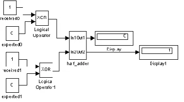
The BMU unit will find the similarities between the received channel symbol and the branch code symbol. Let the received bits are ‘10’ and expected bits are ‘00’ so EX-OR of this will be ‘10’ and in this no. of 1’s is ‘1’ so it will generate the binary equivalent of no. of 1’s which is ‘01’ in this case are shown in Figure 7.
Path metric renormalization unit (PMRU) is used to avoid path metric overflow, add-compare-select unit (ACSU) performs the function called metric rescaling. Since more branch metric is accumulated as steps go on, path metric also increases, which makes memory storing path metrics overflow.
Figure 7 Simulation of branch metric unit (BMU)
Hence path metric rescaling method that subtracts min. metric from all other metrics is suggested to avoid these phenomena. To reduce overhead of ACSU, one removed
[image:4.595.85.274.405.510.2]min. metric selection logic of ACSU and use simple overflow detection unit to rescale path metrics, called path metric renormalization unit(PMRU). This unit will compare each incoming path metrics with constant bits that are ‘01’ here and if incoming path metric bits are greater than constant bits, it will subtract ‘01’ from them and if not, pass the incoming path metric bits as it in output. The fixed value is chosen such that it makes comparator simple and fast. The model of PMRU is shown in Figure 8. The unit adder consists of BMU and PMU unit. It adds branch metrics with their respective path metrics and provides output. Suppose received bits are ‘10’ and expected bits are ‘00’ then branch metric will be ‘01’. Now the path metric is ‘10’ so output of PMU will be ‘01’ this unit will add PMU output with BMU output that will be ‘10’. The unit comparator compares the outputs of two different unit adders and provides min. between them.
Figure 8 Simulation of path metric renormalization unit (PMRU)
It consists of unit adders and mux in it. Depending upon the select line it avails min. value unit adder output as input for next stage. Add-compare–select unit (ACSU) performs addition, comparison and selection operation. For 6-bit message input to convolution encoder, there should be six stages in ACSU. Each stage receives 2-bit. This received bits are compared with expected bits and results are generated which acts as a path metric bits for next stage. Each stage is driven by a clock circuitry. On first clock edge first stage will work. On next clock, second stage will work so after six clocks one will get the output. The complete model of design is shown in Figure 9. The trace back length =32 is used in this design.
[image:4.595.134.491.566.749.2]Figure 10 Decoded symbols using Analog Viterbi decoder
The decoded symbols are plotted in blue stems with circles while the original (unencoded) symbols are plotted in red stems with x's (Figure 10). The red stems of the original signal are shadowed by the blue stems of the decoded signal. Therefore, comparing the red x's with the blue circles indicates that the decoded signal is identical to the original (unencoded) signal.
5. MODIFIED ANALOG VITERBI
DECODER DESIGN
In this work, the analog Viterbi decoder is designed to meet higher throughput, lower gate count, and minimum overall area.
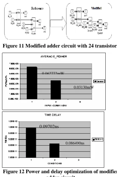
Figure 11 Modified adder circuit with 24 transistors
Figure 12 Power and delay optimization of modifier adder circuit
Design for each block is chosen to obtain optimum performance and maximum throughput. Two major contributions in this design are optimizing the adder unit and PMR unit. General implementation of unit adder requires 36 transistors. The modified design implements the same logic using only 24 transistors. The effect of this is shown on total time delay and power is shown in Figure 11. Figure 12 shows the comparison of modified adder circuit before and after optimization. The power is reduced by 0.031472mW and the delay is reduced by 0.0153ns.
[image:5.595.334.536.170.254.2]Modified unit adder reduces the chip area of overall design to 6612.92µm2. The Path metric renormalization unit (PMRU) is to check for path metric overflow and if it happens, subtract a constant value from it. This block is implemented using three half subtractors and two mux. General implementation of PMR Unit requires three half subtractors and two mux. The same logic can be implemented using one half subtractor, two ex-or gates and two MUXs as shown in Figure 13.
Figure 13 Modified PMR unit
[image:5.595.335.503.325.514.2]The advantages of modified PMR Unit (Figure 14) are reduction in power supply requirement of the design from 0.021731mW to 0.018481mW, Reduction in the operating time of design from 0.15544ns to 0.14759ns. Modified PMR Unit reduces the chip area of overall design to 4920.10µm2.
Figure 14 Power and delay comparison of modified PMR unit
Figure 15 ACSU circuit schematic
An ACSU unit consists of adders, comparators and memory elements in it. For 6-bit message, the no. of stages in ACS unit will be six. Each stage operates on two received bits. As the no. of message bits grown up, the no.
0.021731mW
0.018481 mW 0.15544ns
0.14759ns
0.09702ns
[image:5.595.85.286.345.649.2] [image:5.595.332.540.560.699.2]of stages also increases in same proportion. Each stage operates on a clock edge.
After six clock cycles only one get output for 6-bit message. The ACSU circuit in virtuoso schematic editor is shown in Figure 15. The ACS block consists of BMU, PMR, unit adder, comparator and memory elements in it. The subsystems are integrated to realize the ACSU.
6. RESULTS AND DISCUSSION
The hardware reference model is developed for analog viterbi decoder in both virtuoso schematic and layout editor. Power and area of each block is calculated in virtuoso schematic editor and tabulated in Table 2. The complete design contains 5,800 transistors and 350329.03µm2 area.
In order to compare the performances of the designed analog Viterbi decoder, in this work design and implementation of digital Viterbi decoder is also carried out. The digital version of Viterbi decoder is designed to have the same specifications as that of analog system. The sub systems such as BMU, Path Metric Unit (PMU), Survivor Memory Unit (SMU) and memory are designed, modeled and integrated together. Figure 16 shows the digital Viterbi decoder architecture. The input is 6-bit width to the BMU, as the input data is chosen to be of size 192 bits, 32 cycles are required to load data and computations will progress in each cycle and at the end of 32 cycle 32-bit output is generated for 32x6 soft decision inputs.
Table 2 Power and area report of AVD
Block name Average power
(mW)
Area (µm2)
BM unit 0.031472 712.45
PMR unit 0.018481 3915.12
Unit adder 0.017600 6612.92
Comparator 0.022000 4920.10
BMU calculates the distance between the input and the value present on the path and the PMU considers the two incoming paths and it compares the path and store survivor path value in the memory and corresponding decision bit is
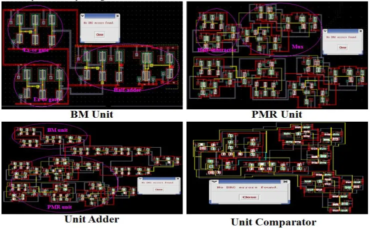
send to the SMU. Finally when the Spath is reached the path metrics are compared and the PMU with the lowest metric is chosen and the output corresponding to the state is decoded as the final output. The HDL model developed for the decoder is verified for its functionality using ModelSim, and is synthesized using Design Compiler targeting 130nm CMOS technology. The area timing and power report are generated for the synthesized design with optimum constrains. The total cell area occupied is 860585.0912 µm2, the design requires 12630 cells, consumes power of 21.0403 mW and operating at a maximum of 62 MHz. Figure 17 shows the layout design of various sub systems of analog Viterbi decoder. Cadence Virtuoso is used to capture the layouts, the physical verification is performed, and DRC check is performed to clear the errors. The captured layouts are integrated to form the top level structure of Analog viterbi Decoder. Table 3 compares the performances of modified analog Viterbi decoder with digital Viterbi decoder.
Figure 16 Block diagram of Viterbi decoder
[image:6.595.352.521.281.346.2]The modified analog Viterbi decoder outperforms digital decoder in terms of operating speed, area and power dissipation. The operating frequency of analog decoder is approximately 100 times faster compared with digital decoder. The power dissipation is reduced by more than 247 times and the transistor count is reduced be more than 8 times. Hence the analog decoding is superior in terms of area, power and speed compared to digital decoding. Nonlinearities and noise analysis are not carried out in this work for comparison. Further the modified analog decoder is optimum in terms of area and power compared with generic analog decoder discussed in [8]. The performances of the modified decoder can be further enhanced with optimization of ACSU logic.
[image:6.595.134.505.522.751.2]Table 3 Performance comparison of Viterbi decoder
7. CONCLUSION
The hardware reference model of the design is developed in HSPICE, virtuoso schematic and layout editor. The HSPICE coding for various blocks of analog viterbi decoder has carried out with encoder. The simulation of design is showing same results as obtained in MATLAB/Simulink. Schematics of BMU, PMRU, ACSU, unit adder and comparator are developed in cadence virtuoso editor. All blocks are integrated to verify functionality. The layouts have developed for BMU, PMRU, unit adder and comparator and checked against DRC rules. The performances of modified analog Viterbi decoder are compared with digital decoder as well as generic analog decoder. It is proved that with proper selection and design of subsystems, the power and area can be optimized. From the results obtained, the proposed decoder operates at a frequency of 412 MHz and consumes power less than 86µW. The designed decoder is suitable for hybrid OFDM architecture. The decoder logic is designed using 0.13 micron CMOS technology, hence there is a restriction to the maximum operating frequency, adopting 65 nm technology, the operating frequency can be improved, it is required to address power dissipation and need to verify the design using signoff tools.
8. ACKNOWLEDGEMENT
The authors would like to thank Dr. CP Raj for their valuable suggestions and inputs provided. The authors would like to acknowledge Dr. NJR Muniraj for the support extended during this work.
9. REFERENCES
[1] Sangwook Suh, Low-Power Discrete Fourier Transform and Soft-Decision Viterbi Decoder For Ofdm Receivers, Doctor of Philosophy in the School of Electrical and Computer Engineering, Georgia Institute of Technology, December 2011
[2] Barry J. R., Messerschmitt D. G., Lee E. A., Digital Communication. Springer, 2003.
[3] Batra A. et al., ’Physical layer proposal for IEEE 802.15 task group 3a’, IEEE P802.15-03/142r2, May 2003
[4] Janne Maunu, Mika Laiho, Tero Koivisto, Kati Virtanen, Mikko P¨ank¨a¨al¨a and Ari Paasio, Mixed-Signal Viterbi Decoder for a MB-OFDM Receiver, Proceedings of the 2008 IEEE international conference on ultra-wideband (ICUWB2008), vol. 3
[5] Sung-Woo Choi, Sang-Sung Choi, ’200Mbps Viterbi decoder for UWB’, Proceedings of ICACT 2005, vol 2, pp. 904-907, February 2005
[6] Chawla R., Bandyopadhyay A., Srinivasan V., and Hasler P., “A 531 nW/MHz, 128x32 current-mode programmable analog vector-matrix multiplier with over 2 decades of linearity,” in IEEE Custom Integrated Circuits Conference, pp. 651-654, 2004. [7] Hall T. S., Twigg C. M, Gray J. D., Hasler P.,
Anderson D. V., “Large-scale field-programmable analog arrays for analog signal processing,” IEEE Transactions on Circuits and Systems I: Regular Papers, vol. 52, no. 11, pp. 2298-2307, 2005. [8] Demosthenous A., Taylor J., ’A 100-Mb/s 2.8-V
CMOS Current-Mode Analog Viterbi Decoder’, IEEE Journal of Solid-State Circuits, vol 37, No. 7, July 2002, pp. 904-910.
[9] Shakiba M. H., D. A. Johns, Martin K. W., ’An Integrated 200-MHz 3.3-V BiCMOS CLASS-IV Partial Response Analog Viterbi Decoder’, IEEE Journal of Solid-State Circuits, Vol. 33, Jan. 1998, pp. 61 - 75.
[10]He. K., Cauwenberghs G., ’An Integrated 64-state Parallel Analog Viterbi Decoder’, Proceedings of the IEEE International Symposium on Circuits and Systems, May 2000, pp. IV.761-IV.764.
[11]Hemati S. and Banihashemi A. H., “Full CMOS min-sum analog iterative decoder,” in Proc. IEEE Int. Symp. Inf. Theory, 2003, p. 347.
[12]Gaudet V. C. and Gulak P. G., “A 13.3-Mb/s 0.35-_ m CMOS analog turbo decoder IC with a configurable interleaver,” IEEE J. Solid-StateCircuits, vol. 38, no. 11, pp. 2010–2015, Nov. 2003.
[13]Winstead C., Dai J., Yu S., Myers C., Harrison R. R., and Schlegel C., “CMOS analog map decoder for (8,4) Hamming code,” IEEE J. Solid-State Circuits, vol. 39, no. 1, pp. 122–131, Jan. 2004.
[14]Vogrig D., Gerosa A., Neviani A., Amat A. G. I., Montorsi G., and Benedetto, S., “A 0.35 _ mCMOS analog turbo decoder for the 40-bit rate 1/3 UMTS channel code,” IEEE J. Solid-State Circuits, vol. 40, no. 3, pp. 753–762, Mar. 2005.
[15]Winstead C., Nguyen N., Gaudet V. C., and Schlegel C., “Low-voltage CMOS circuits for analog iterative decoders,” IEEE Trans. Circuits Syst. I, Reg. Papers, vol. 53, no. 4, pp. 829–841, Apr. 2006.
[16]Barry J. R., Messerschmitt D. G., Lee E. A., Digital Communication. Springer, 2003.
[17]Hagenauer J., Moerz M., Schaefer A., "Analog decoders and receivers for high speed applications," in IEEE International Zurich Seminar on Broadband Communications, pp. 3-1-3-8, 2002.
[18]Loeliger H. A., Lustenberger F., Helfenstein M., Tarkoy F., "Probability propagation and decoding in analog VLSI," IEEE Transactions on Information Theory, vol. 47, no. 2, pp. 837-843, 2001.
decoding algorithm," IEEE Transactions on Circuits and Systems I: Fundamental Theory and Applications, vol. 50, no. 10, pp. 1256-1269, 2003. [20]Acampora A., Gilmore R., “Analog Viterbi Decoding
for High Speed Digital Satellite Channels,” IEEE Transactions on Communications, vol. 26, no. 10, pp. 1463-1470, 1978.
[21]Demosthenous A., Taylor J., "Effects of signal-dependant errors on the performance of switched-current Viterbi decoders," IEEE Transactions on Circuits and Systems I: Fundamental Theory and Applications, vol. 48, no. 10, pp. 1225–1228, 2001. [22]He K., Cauwenberghs G., "An area-efficient analog
VLSI architecture for state parallel Viterbi decoding," IEEE International Symposium on Circuits and Systems, pp. 432-435, 1999.
[23]Wen-Ta Lee, Ming-Jlun, Yuh-Shyan Hwang and Jiann-Jong Chen “IC Design of a New Decision Device for Analog Viterbi Decoder” Institute of Computer and Communication, National Taipei University of Technology Taipei, Taiwan, R.O.C., 2006.
[24]Viterbi A. J., “Convolution codes and their performance in communication systems,” IEEE Transaction on Communications, vol.com-19, pp. 751 to 771, October 1971.
![Figure 2 Baseband processor architecture of OFDM [4]](https://thumb-us.123doks.com/thumbv2/123dok_us/8100519.787692/2.595.122.502.555.636/figure-baseband-processor-architecture-ofdm.webp)
![Figure 4 Convolutional encoder with rate ½ [24]](https://thumb-us.123doks.com/thumbv2/123dok_us/8100519.787692/3.595.85.285.377.642/figure-convolutional-encoder-rate.webp)