4 x 46 W multifunction quad power amplifier
with built-in diagnostics features
Features
■ MOSFET output power stage
■ High output power capability 4 x 25 W/4 @ 14.4 V, 1 kHz, 10 % THD
■ Max. output power 4 x 68 W/2 , 4 x 42 W/4 @ 14.4 V
■ Full I2C bus driving: – Standby
– Independent front/rear soft play/mute – Selectable gain 30 dB - 16 dB – I2C bus digital diagnostics
■ Full fault protection
■ DC offset detection
■ Four independent short circuit protection
■ Clipping detector (2 % / 10 %)
■ Standby/mute pin
■ ESD protection
Description
The TDA7562B is a new BCD technology quad bridge type of car radio amplifier in Flexiwatt27 package specially intended for car radio applications.
Thanks to the DMOS output stage the TDA7562B has a very low distortion allowing a clear powerful sound.
This device is equipped with a full diagnostics array that communicates the status of each speaker through the I2C bus.
The possibility to control the configuration and behavior of the device by means of the I2C bus makes TDA7562B a very flexible machine.
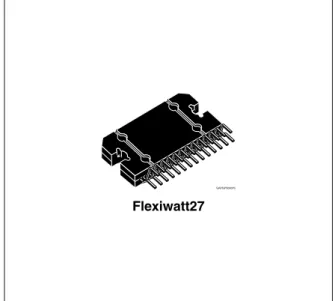
Flexiwatt27
'!0'03
Table 1. Device summary
Order code Package Packing
Contents
1
Block diagram and application and test circuit . . . 5
1.1
Block diagram . . . 5
1.2
Application and test circuit . . . 5
2
Pin description . . . 6
3
Electrical specifications . . . 7
3.1
Absolute maximum ratings . . . 7
3.2
Thermal data . . . 7
3.3
Electrical characteristics . . . 8
3.4
Electrical characteristics curves . . . 11
4
Diagnostics functional description . . . 13
4.1
Turn-on diagnostic . . . 13
4.2
Permanent diagnostics . . . 15
4.3
Output DC offset detection . . . 16
4.4
AC diagnostic . . . 17
4.5
Multiple faults . . . 18
4.6
Faults availability . . . 18
4.7
I
2C Programming/reading sequence . . . 19
4.8
Fast muting . . . 19
5
I
2C bus interface . . . 20
5.1
Data validity . . . 20
5.2
Start and stop conditions . . . 20
5.3
Byte format . . . 20
5.4
Acknowledge . . . 20
6
Software specifications . . . 22
7
Examples of bytes sequence . . . 27
8
Package information . . . 28
List of tables
Table 1. Device summary . . . 1
Table 2. Absolute maximum ratings . . . 7
Table 3. Thermal data. . . 7
Table 4. Electrical characteristics . . . 8
Table 5. Double fault table for turn on diagnostic . . . 18
Table 6. IB1 . . . 22
Table 7. IB2 . . . 23
Table 8. DB1 . . . 23
Table 9. DB2 . . . 24
Table 10. DB3 . . . 25
Table 11. DB4 . . . 26
List of figures
Figure 1. Block diagram . . . 5
Figure 2. Application and test circuit . . . 5
Figure 3. Pin connection (top view) . . . 6
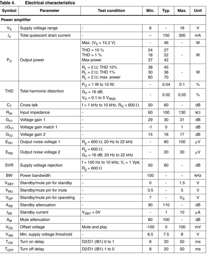
Figure 4. Output power vs. supply voltage (4) . . . 11
Figure 5. Output power vs. supply voltage (2) . . . 11
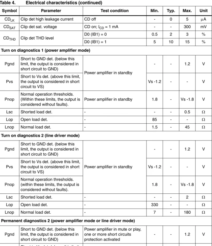
Figure 6. Distortion vs. output power (4) . . . 11
Figure 7. Distortion vs. output power (2) . . . 11
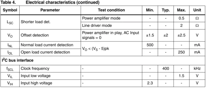
Figure 8. Distortion vs. frequency (4) . . . 11
Figure 9. Distortion vs. frequency (2) . . . 11
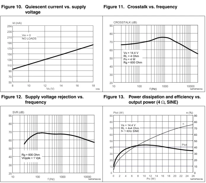
Figure 10. Quiescent current vs. supply voltage . . . 12
Figure 11. Crosstalk vs. frequency . . . 12
Figure 12. Supply voltage rejection vs. frequency . . . 12
Figure 13. Power dissipation and efficiency vs. output power (4 W, SINE) . . . 12
Figure 14. Power dissipation vs. average output power (audio program simulation, 4 W) . . . 12
Figure 15. Power dissipation vs. average output power (audio program simulation, 2 W) . . . 12
Figure 16. Turn-on diagnostic: working principle . . . 13
Figure 17. SVR and output behavior (case 1: without turn-on diagnostic). . . 14
Figure 18. SVR and output pin behavior (case 2: with turn-on diagnostic) . . . 14
Figure 19. Thresholds for short to GND/VS . . . 14
Figure 20. Thresholds for short across the speaker/open speaker . . . 15
Figure 21. Thresholds for line-drivers . . . 15
Figure 22. Restart timing without diagnostic enable (permanent) . . . 16
Figure 23. Restart timing with diagnostic enable (permanent). . . 16
Figure 24. Current detection: Load impedance magnitude |Z| Vs. output peak voltage of the sinus . . 17
Figure 25. Data validity on the I2C bus . . . 20
Figure 26. Timing diagram on the I2C Bus. . . 21
Figure 27. Timing acknowledge clock pulse . . . 21
1
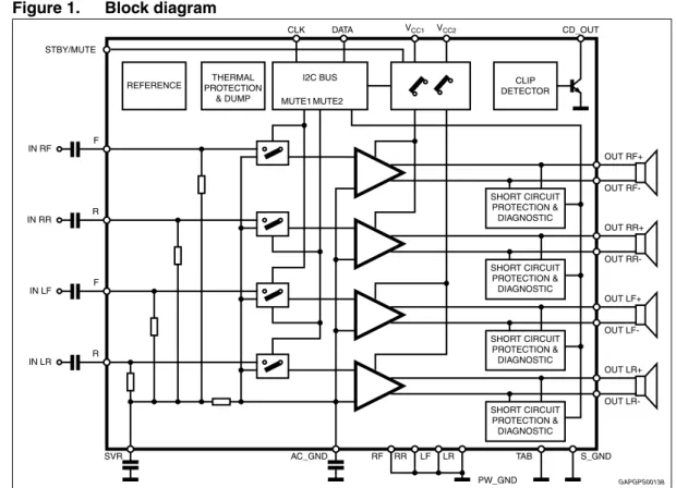
Block diagram and application and test circuit
1.1 Block
diagram
Figure 1. Block diagram
1.2
Application and test circuit
Figure 2. Application and test circuit
'!0'03 )#"53 4(%2-!, 02/4%#4)/. $5-0 2%&%2%.#% #,)0 $%4%#4/2 & 2 &
362 !#?'.$ 2& 22 ,& ,2 4!" 3?'.$
2 ).2& 34"9-54% ).22 ).,& ).,2 /54,2 07?'.$ /54,2 /54,& /54,& /5422 /5422 /542& /542& -54% -54% 3(/24#)2#5)4 02/4%#4)/. $)!'./34)# 3(/24#)2#5)4 02/4%#4)/. $)!'./34)# 3(/24#)2#5)4 02/4%#4)/. $)!'./34)# 3(/24#)2#5)4 02/4%#4)/. $)!'./34)# 6## 6##
$!4! #$?/54
#,+
'!0'03
).2& #M&
).22 #M&
/542&
/5422
).,& #M&
).,2 #M&
/54,& /54,2 # M& # M& 4!" + 6CC 6CC # M& 666## # M& $!4! )#"53 #,+ 3'.$ #$/54 6
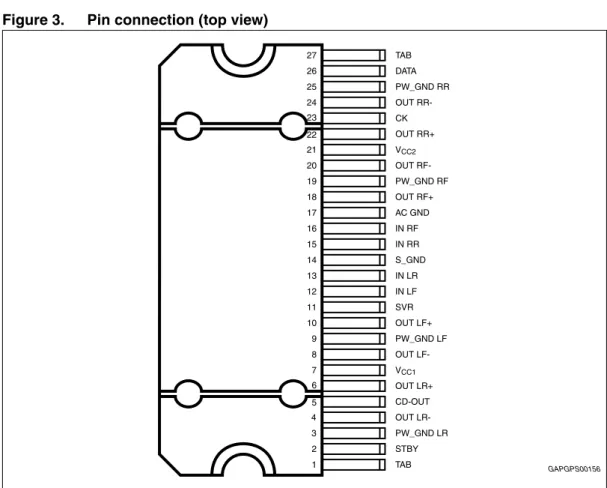
2 Pin
description
Figure 3. Pin connection (top view)
4!" 34"9 07?'.$,2 /54,2 #$/54 /54,2 6##
/54,& 07?'.$,& /54,& 362 ).,& ).,2 3?'.$ ).22 ).2& !#'.$ /542& 07?'.$2& /542& 6##
#+ /5422
/5422 07?'.$22 $!4! 4!"
3 Electrical
specifications
3.1
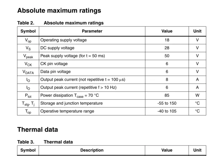
Absolute maximum ratings
3.2 Thermal
data
Table 2. Absolute maximum ratings
Symbol Parameter Value Unit
Vop Operating supply voltage 18 V
VS DC supply voltage 28 V
Vpeak Peak supply voltage (for t = 50 ms) 50 V
VCK CK pin voltage 6 V
VDATA Data pin voltage 6 V
IO Output peak current (not repetitive t = 100 s) 8 A
IO Output peak current (repetitive f > 10 Hz) 6 A
Ptot Power dissipation Tcase = 70 °C 85 W
Tstg, Tj Storage and junction temperature -55 to 150 °C
Top Operative temperature range -40 to 105 °C
Table 3. Thermal data
Symbol Description Value Unit
3.3 Electrical
characteristics
Refer to the test circuit, VS = 14.4 V; RL = 4 ; f = 1 kHz; GV = 30 dB; Tamb = 25 °C; unless otherwise specified.
Table 4. Electrical characteristics
Symbol Parameter Test condition Min. Typ. Max. Unit
Power amplifier
VS Supply voltage range - 8 - 18 V
Id Total quiescent drain current - -- 150 300 mA
PO Output power
Max. (VS = 15.2 V) - 46 - W
THD = 10 % THD = 1 % Max power
24 18 37
27 22 42
- W
RL = 2 ; THD 10% RL = 2 ; THD 1% RL = 2 ; max. power
38 30 60
45 36 70
- W
THD Total harmonic distortion
PO = 1 W to 10 W; - 0.04 0.1 %
GV = 16 dB;
VO = 0.1 to 5 VRMS - 0.02 0.05 %
CT Cross talk f = 1 kHz to 10 kHz, RG = 600 50 60 - dB
RIN Input impedance - 60 100 130 k
GV1 Voltage gain 1 - 29 30 31 dB
GV1 Voltage gain match 1 - -1 0 1 dB
GV2 Voltage gain 2 - 15 16 17 dB
EIN1 Output noise voltage 1 Rg = 600 20 Hz to 22 kHz - 60 100 V EIN2 Output noise voltage 2 Rg = 600 ;
GV = 16 dB; 20 Hz to 22 kHz - 20 30 V SVR Supply voltage rejection f = 100 Hz to 10 kHz; Vr = 1 Vpk;
Rg = 600 50 60 - dB
BW Power bandwidth - 100 - - kHz
VSBY Standby/mute pin for standby - 0 - 1.5 V
VMU Standby/mute pin for mute - 3.5 - 5 V
VOP Standby/mute pin for operating - 7 - VS V
ASB Standby attenuation - 90 110 - dB
ISB Standby current VSBY = 0V - 1 10 A
AM Mute attenuation - 80 100 - dB
VOS Offset voltage Mute and play -100 0 100 mV
VAM Min. supply voltage threshold - 6.5 7.5 8 V
TON Turn on delay D2/D1 (IB1) 0 to 1 8 20 50 ms
CDLK Clip det high leakage current CD off - 0 5 A
CDSAT Clip det sat. voltage CD on; ICD = 1 mA - - 300 mV
CDTHD Clip det THD level
D0 (IB1) = 0 0.5 2 3 %
D0 (IB1) = 1 5 10 15 %
Turn on diagnostics 1 (power amplifier mode)
Pgnd
Short to GND det. (below this limit, the output is considered in short circuit to GND)
Power amplifier in standby
- - 1.2 V
Pvs
Short to Vs det. (above this limit, the output is considered in short circuit to VS)
Vs -1.2 - - V
Pnop
Normal operation thresholds. (Within these limits, the output is considered without faults).
Power amplifier in standby 1.8 - Vs -1.8 V
Lsc Shorted load det. - - - 0.5
Lop Open load det. - 85 - -
Lnop Normal load det. - 1.5 - 45
Turn on diagnostics 2 (line driver mode)
Pgnd
Short to GND det. (below this limit, the output is considered in short circuit to GND)
Power amplifier in standby
- - 1.2 V
Pvs
Short to Vs det. (above this limit, the output is considered in short circuit to VS)
Vs -1.2 - - V
Pnop
Normal operation thresholds. (within these limits, the output is considered without faults).
1.8 - Vs -1.8 V
Lsc Shorted load det. - - - 2
Lop Open load det. - 330 - -
Lnop Normal load det. - 7 - 180
Permanent diagnostics 2 (power amplifier mode or line driver mode)
Pgnd
Short to GND det. (below this limit, the output is considered in short circuit to GND)
Power amplifier in mute or play, one or more short circuits protection activated
- - 1.2 V
Pvs
Short to Vs det. (above this limit, the output is considered in short circuit to VS)
- Vs -1.2 - - V
Pnop
Normal operation thresholds. (Within these limits, the output is considered without faults).
- 1.8 - Vs -1.8 V
Table 4. Electrical characteristics (continued)
LSC Shorter load det. Power amplifier mode - - 0.5
Line driver mode - - 2
VO Offset detection Power amplifier in play, AC Input
signals = 0 ±1.5 ±2 ±2.5 V
INL Normal load current detection
VO < (VS - 5)pk
500 - - mA
IOL Open load current detection - - 250 mA
I2C bus interface
fSCL Clock frequency - - 400 - kHz
VIL Input low voltage - - - 1.5 V
VIH Input high voltage - 2.3 - - V
Table 4. Electrical characteristics (continued)
3.4 Electrical
characteristics
curves
Figure 4. Output power vs. supply voltage
(4)
Figure 5. Output power vs. supply voltage
(2)
Figure 6. Distortion vs. output power (4) Figure 7. Distortion vs. output power (2)
Figure 8. Distortion vs. frequency (4) Figure 9. Distortion vs. frequency (2)
6S6 0O7 2,/HM F+(Z 4($ 4($ 0OMAX '!0'03 6S6 0O7 2,/HM F+(Z 4($ 4($ 0OMAX '!0'03 3R: 7+' I .+] 9V 9 5/ 2KP I .+] '!0'03 '!0'03 3R: 7+' I .+] 9V 9 5/ 2KP I .+] '!0'03 I+] 7+' 9V 9 5/ 2KP 3R : '!0'03 I+] 7+' 9V 9 5/ 2KP 3R :
Figure 10. Quiescent current vs. supply voltage
Figure 11. Crosstalk vs. frequency
Figure 12. Supply voltage rejection vs. frequency
Figure 13. Power dissipation and efficiency vs.
output power (4, SINE)
Figure 14. Power dissipation vs. average output
power (audio program simulation, 4)
Figure 15. Power dissipation vs. average output
power (audio program simulation, 2)
'!0'03 9V9 ,GP$ 9LQ 12/2$'6 '!0'03 I+] &52667$/.G% 9V 9 5/ 2KP 3R : 5J 2KP '!0'03 I+] 695G% 5J 2KP 9ULSSOH 9SN '!0'03 3R: 3WRW: Q Q 3WRW 9V 9 5/ [2KP I .+]6,1( '!0'03 3R: 3WRW: &/,3 67$57 9V 9 5/ [2KP *$866,$112,6( '!0'03 3R: 3WRW: 9V 9 5/ [2KP *$866,$112,6( &/,3 67$57
4
Diagnostics functional description
4.1 Turn-on
diagnostic
It is activated at the turn-on (stand-by out) under I2C bus request. Detectable output faults are:
– Short to GND – Short to VS
– Short across the speaker – Open speaker
To verify if any of the above misconnections are in place, a subsonic (inaudible) current pulse (Figure 16) is internally generated, sent through the speaker(s) and sunk back.The Turn On diagnostic status is internally stored until a successive diagnostic pulse is requested (after a I2C reading).
If the "standby out" and "diag. enable" commands are both given through a single programming step, the pulse takes place first (power stage still in stand-by mode, low, outputs = high impedance).
Afterwards, when the Amplifier is biased, the PERMANENT diagnostic takes place. The previous Turn-on state is kept until a short appears at the outputs.
Figure 16. Turn-on diagnostic: working principle
Figure 17 and 18 show SVR and output waveforms at the turn-on (standby out) with and without turn-on diagnostic.
,VRXUFH
9Va9
&+ &+
,VLQN
WPV ,P$
,VLQN ,VRXUFH
aPV 0HDVXUHWLPH
Figure 17. SVR and output behavior (case 1: without turn-on diagnostic)
Figure 18. SVR and output pin behavior (case 2: with turn-on diagnostic)
The information related to the outputs status is read and memorized at the end of the current pulse top. The acquisition time is 100 ms (typ.). No audible noise is generated in the process. As for short to GND / Vs the fault-detection thresholds remain unchanged from 30 dB to 16 dB gain setting. They are as follows:
Figure 19. Thresholds for short to GND/VS
Concerning short across the speaker / open speaker, the threshold varies from 30 dB to 16 dB gain setting, since different loads are expected (either normal speaker's impedance or high impedance). The values in case of 30 dB gain are as follows:
"IASPOWER AMPT URNON
T
$IAGNOSTIC %NABLE 0ERMANENT
0ERMANENT$IAGNOSTICSDATAOUPUT PERMITTEDTIME 0ERMANENTDIAGNOSTIC ACQUISITIONTIMEMS4YP
)#"$!4!
6SVR /UT
&!5,4
EVENT 2EAD$ATA
'!0'03
"IASPOWERAMP TURNON PERMITTE DT IME 4U RNOND IAGNOSTIC ACQU ISI TIONTIM EMS 4YP
T
2EAD$ATA
0ERMANENTDIAGN OST IC ACQUI SIT IONTIMEMS 4YP
0ERMANENT$IAGNO ST ICS DAT AOUT PUT PERMITTE DTIME $IAGNOST IC%NABLE
4UR NON
4URNON $IAGN OST ICS DATAOUT PU T PER MITT EDTI ME
)#"$!4!
6SVR /UT
$IAGN OST IC% NABLE 0ERMAN ENT
&!5,4 EVENT
'!0'03
3#TO'.$ X 3#TO6S
6 6 636 63
X .ORMAL/PERATION
6 636
Figure 20. Thresholds for short across the speaker/open speaker
If the Line-Driver mode (Gv= 16 dB and line driver mode diagnostic = 1) is selected, the
same thresholds will change as follows:
Figure 21. Thresholds for line-drivers
4.2 Permanent
diagnostics
Detectable conventional faults are: – short to GND
– short to Vs
– short across the speaker
The following additional features are provided: – output offset detection
– AC diagnostic
The TDA7562B has 2 operating statuses:
1. Restart mode. The diagnostic is not enabled. Each audio channel operates independently from each other. If any of the a.m. faults occurs, only the channel(s) interested is shutdown. A check of the output status is made every 1 ms (Figure 22). Restart takes place when the overload is removed.
2. Diagnostic mode. It is enabled via I2C bus and self activates if an output overload (such to cause the intervention of the short-circuit protection) occurs to the speakers outputs. Once activated, the diagnostics procedure develops as follows (Figure 23):
– To avoid momentary re-circulation spikes from giving erroneous diagnostics, a check of the output status is made after 1ms: if normal situation (no overloads) is detected, the diagnostic is not performed and the channel returns back active. – Instead, if an overload is detected during the check after 1 ms, then a diagnostic
cycle having a duration of about 100 ms is started.
– After a diagnostic cycle, the audio channel interested by the fault is switched to restart mode. The relevant data are stored inside the device and can be read by the microprocessor. When one cycle has terminated, the next one is activated by an I2C reading. This is to ensure continuous diagnostics throughout the car-radio operating time.
– To check the status of the device a sampling system is needed. The timing is chosen at microprocessor level (over half a second is recommended).
3#ACROSS,OAD X /PEN,OAD
6 7 7 )NFINITE X
.ORMAL/PERATION
7 7
'!0'03
3#ACROSS,OAD X /PEN,OAD
7 7 7 INFINITE X
.ORMAL/PERATION
7 7
Figure 22. Restart timing without diagnostic enable (permanent)
Each 1 ms time, a sampling of the fault is done
Figure 23. Restart timing with diagnostic enable (permanent)
4.3
Output DC offset detection
Any DC output offset exceeding ±2V are signalled out. This inconvenient might occur as a consequence of initially defective or aged and worn-out input capacitors feeding a DC component to the inputs, so putting the speakers at risk of overheating.
This diagnostic has to be performed with low-level output AC signal (or Vin = 0).
The test is run with selectable time duration by microprocessor (from a "start" to a "stop" command):
Start = Last reading operation or setting IB1 - D5 - (OFFSET enable) to 1 Stop = Actual reading operation
Excess offset is signalled out if persistent throughout the assigned testing time. This feature is disabled if any overloads leading to activation of the short-circuit protection occurs in the process.
T
M3 M3 M3 M3 M3
/VERCUR RENTAND SHOR T CIRCUIT PROTECT IONI NTERVENT ION
IESHOR TCIRCUI TT O'.$
3HOR TCIRCUI TREMOVED
/UT
'!0'03
T /VERCURRENT ANDSHORT
CIRCUITPROTECTI ON IN TERVENTI ON IES HORTC IRCUI TTO'.$
3HO RTCIRCUIT REMOVED
M3 M3 M3 M3
4.4 AC
diagnostic
It is targeted at detecting accidental disconnection of tweeters in 2-way speaker and, more in general, presence of capacitive (AC) coupled loads.
This diagnostic is based on the notion that the overall speaker's impedance (woofer + parallel tweeter) will tend to increase towards high frequencies if the tweeter gets
disconnected, because the remaining speaker (woofer) would be out of its operating range (high impedance). The diagnostic decision is made according to peak output current thresholds, as follows:
Iout > 500 mApk = normal status Iout < 250 mApk = open tweeter
To correctly implement this feature, it is necessary to briefly provide a signal tone (with the amplifier in "play") whose frequency and magnitude are such to determine an output current higher than 500 mApk in normal conditions and lower than 250 mApk should the parallel tweeter be missing. The test has to last for a minimum number of 3 sine cycles starting from the activation of the AC diagnostic function IB2 < D2 > 0 up to the I2C reading of the results (measuring period). To confirm presence of tweeter, it is necessary to find at least 3 current pulses over 500 mA over all the measuring period, else an "open tweeter" message will be issued.
The frequency / magnitude setting of the test tone depends on the impedance
characteristics of each specific speaker being used, with or without the tweeter connected (to be calculated case by case). High-frequency tones (> 10 kHz) or even ultrasonic signals are recommended for their negligible acoustic impact and also to maximize the impedance module's ratio between with tweeter-on and tweeter-off.
Figure 24 shows the Load Impedance as a function of the peak output voltage and the relevant diagnostic fields.
This feature is disabled if any overloads leading to activation of the short-circuit protection occurs in the process.
Figure 24. Current detection: Load impedance magnitude |Z| Vs. output peak
voltage of the sinus
6OUT 0EAK ,O AD\Z\/HM
)OUTPEAK M! )OUTPEAK M! ,OWCURRENTDETECTIONAREA
/PENLOAD $OFTHE$"XBYRES
(IGHCURRENTDETECTIONAREA .ORMALLOAD $OFTHE$"XBYTES
)"$
4.5 Multiple
faults
When more misconnections are simultaneously in place at the audio outputs, it is guaranteed that at least one of them is initially read out. The others are notified after successive cycles of I2C reading and faults removal, provided that the diagnostic is enabled. This is true for both kinds of diagnostic (Turn-on and Permanent).
The table below shows all the couples of double-fault possible. It should be taken into account that a short circuit with the 4 ohm speaker unconnected is considered as double fault.
4.6 Faults
availability
All the results coming from I2C Bus, by read operations, are the consequence of measurements inside a defined period of time. If the fault is stable throughout the whole period, it will be sent out. This is true for DC diagnostic (Turn-on and Permanent), for Offset Detector, for AC Diagnostic (the low current sensor needs to be stable to confirm the Open tweeter).
To guarantee always resident functions, every kind of diagnostic cycles (Turn-on, Permanent, Offset, AC) will be reactivate after any I2C reading operation. So, when the micro reads the I2C, a new cycle will be able to start, but the read data will come from the previous diag. cycle (i.e. The device is in Turn-on state, with a short to GND, then the short is removed and micro reads I2C. The short to GND is still present in bytes, because it is the result of the previous cycle. If another I2C reading operation occurs, the bytes do not show the short). In general to observe a change in Diagnostic bytes, two I2C reading operations are necessary.
Table 5. Double fault table for turn on diagnostic
- S. GND (so) S. GND (sk) S. Vs S. Across L. Open L.
S. GND (so)(1)
1. S. GND (so) / S. GND (sk) in the above table make a distinction according to which of the 2 outputs is shorted to ground (test-current source side= so, test-current sink side = sk). More precisely, in channels LF and LR, so = CH+, sk = CH-; in channels LR and RF, so = CH-, SK = CH+.
S. GND S. GND S. Vs + S.
GND S. GND S. GND
S. GND (sk)(1) / S. GND S. Vs S. GND Open Load(2)
2. In Permanent Diagnostic the table is the same, with only a difference concerning Open Load, which is not among the recognizable faults. Should an Open Load be present during the device's normal working, it would be detected at a subsequent Turn on Diagnostic cycle (i.e. at the successive Car Radio Turn on).
S. Vs / / S. Vs S. Vs S. Vs
S. Across L. / / / S. Across L. N.A.
4.7 I
2
C Programming/reading sequence
A correct turn on/off sequence respectful of the diagnostic timings and producing no audible noises could be as follows (after battery connection):
TURN-ON: (STANDBY OUT + DIAG ENABLE) --- 500 ms (min) --- MUTING OUT TURN-OFF: MUTING IN --- 20 ms --- (DIAG DISABLE + STANDBY IN)
Car Radio Installation: DIAG ENABLE (write) --- 200 ms --- I2C read (repeat until All faults disappear).
AC TEST: FEED H.F. TONE -- AC DIAG ENABLE (write) --- WAIT > 3 CYCLES --- I2C read (repeat I2C reading until tweeter-off message disappears).
OFFSET TEST: Device in Play (no signal) -- OFFSET ENABLE - 30ms - I2C reading (repeat I2C reading until high-offset message disappears).
4.8 Fast
muting
The muting time can be shortened to less than 1.5 ms by setting (IB2) D5 = 1. This option can be useful in transient battery situations (i.e. during car engine cranking) to quickly turnoff the amplifier for avoiding any audible effects caused by noise/transients being injected by preamp stages. The bit must be set back to “0” shortly after the mute transition.
5 I
2
C bus interface
Data transmission from microprocessor to the TDA7562B and voice-overs takes place through the 2 wires I2C bus interface, consisting of the two lines SDA and SCL (pull-up resistors to positive supply voltage must be connected).
5.1 Data
validity
As shown by Figure 25, the data on the SDA line must be stable during the high period of the clock.
The high and low state of the data line can only change when the clock signal on the SCL line is low.
5.2
Start and stop conditions
As shown by Figure 26 a start condition is a high to low transition of the SDA line while SCL is high.
The stop condition is a low to high transition of the SDA line while SCL is high.
5.3 Byte
format
Every byte transferred to the SDA line must contain 8 bits. Each byte must be followed by an acknowledge bit. The MSB is transferred first.
5.4 Acknowledge
The transmitter* puts a resistive high level on the SDA line during the acknowledge clock pulse (see Figure 27). The receiver** the acknowledges has to pull-down (LOW) the SDA line during the acknowledge clock pulse, so that the SDA line is stable LOW during this clock pulse.
* Transmitter
– master (µP) when it writes an address to the TDA7562B
– slave (TDA7562B) when the µP reads a data byte from TDA7562B ** Receiver
– slave (TDA7562B) when the µP writes an address to the TDA7562B – master (µP) when it reads a data byte from TDA7562B
Figure 25. Data validity on the I2C bus
3$!
3#,
$!4!,).% 34!",%$!4!
6!,)$
#(!.'% $!4!
Figure 26. Timing diagram on the I2C Bus
Figure 27. Timing acknowledge clock pulse
3#,
3$!
34!24
)#"53
34/0 '!0'03
3#,
-3"
3$!
34!24 !#+./7,%$'-%.4&2/-2%#%)6%2
6 Software
specifications
All the functions of the TDA7562B are activated by I2C interface.
The bit 0 of the "ADDRESS BYTE" defines if the next bytes are write instruction (from P to TDA7562B) or read instruction (from TDA7562B to µP).
X = 0 write to device X = 1 read from device
If R/W = 0, the P sends 2 "Instruction bytes": IB1 and IB2.
D7 D0
1 1 0 1 1 0 0 X D8 Hex
Table 6. IB1
Bit Instruction decoding bit
D7 0
D6 Diagnostic enable (D6 = 1) Diagnostic defeat (D6 = 0) D5 Offset Detection enable (D5 = 1)
Offset Detection defeat (D5 = 0)
D4
Front Channel Gain = 30 dB (D4 = 0) Gain = 16 dB (D4 = 1)
D3
Rear Channel Gain = 30 dB (D3 = 0) Gain = 16 dB (D3 = 1) D2 Mute front channels (D2 = 0)
Unmute front channels (D2 = 1) D1 Mute rear channels (D1 = 0)
Unmute rear channels (D1 = 1) D0 CD 2% (D0 = 0)
If R/W = 1, the TDA7562B sends 4 "Diagnostics Bytes" to mP: DB1, DB2, DB3 and DB4.
Table 7. IB2
Bit Instruction decoding bit
D7 0
D6 0
D5 Normal muting time (D5 = 0) Fast muting time (D5 = 1)
D4 Standby on - Amplifier not working - (D4 = 0) Standby off - Amplifier working - (D4 = 1) D3 Power amplifier mode diagnostic (D3 = 0)
Line driver mode diagnostic (D3 = 1)
D2 Current detection diagnostic enabled (D2 = 1) Current detection diagnostic defeat (D2 = 0)
D1 0
D0 0
Table 8. DB1
Bit Instruction decoding bit
D7 Thermal warning active (D7 = 1)
D6 Diag. cycle not activated or not terminated (D6 = 0) Diag. cycle terminated (D6 = 1)
D5
Channel LF Current detection
Output peak current < 250 mA - Open load (D5 = 1) Output peak current > 500 mA - Open load (D5 = 0) D4
Channel LF
Turn-on diagnostic (D4 = 0) Permanent diagnostic (D4 = 1) D3
Channel LF
Normal load (D3 = 0) Short load (D3 = 1)
D2
Channel LF
Turn-on diag.: No open load (D2 = 0) Open load detection (D2 = 1)
Offset diag.: No output offset (D2 = 0) Output offset detection (D2 = 1) D1
Channel LF
No short to Vcc (D1 = 0) Short to Vcc (D1 = 1) D0
Channel LF
No short to GND (D1 = 0) Short to GND (D1 = 1)
Table 9. DB2
Bit Instruction decoding bit
D7 Offset detection not activated (D7 = 0) Offset detection activated (D7 = 1) D6 Current sensor not activated (D6 = 0)
Current sensor activated (D6 = 1)
D5
Channel LR Current detection
Output peak current < 250 mA - Open load (D5 = 1) Output peak current > 500 mA - Open load (D5 = 0)
D4
Channel LR
Turn-on diagnostic (D4 = 0) Permanent diagnostic (D4 = 1)
D3
Channel LR
Normal load (D3 = 0) Short load (D3 = 1)
D2
Channel LR
Turn-on diag.: No open load (D2 = 0) Open load detection (D2 = 1)
Permanent diag.: No output offset (D2 = 0) Output offset detection (D2 = 1)
D1
Channel LR
No short to Vcc (D1 = 0) Short to Vcc (D1 = 1)
D0
Channel LR
No short to GND (D1 = 0) Short to GND (D1 = 1)
Table 10. DB3
Bit Instruction decoding bit
D7 Stand-by status (= IB1 - D4) D6 Diagnostic status (= IB1 - D6)
D5
Channel RF Current detection
Output peak current < 250 mA - Open load (D5 = 1) Output peak current > 500 mA - Open load (D5 = 0)
D4
Channel RF
Turn-on diagnostic (D4 = 0) Permanent diagnostic (D4 = 1)
D3
Channel RF
Normal load (D3 = 0) Short load (D3 = 1)
D2
Channel RF
Turn-on diag.: No open load (D2 = 0) Open load detection (D2 = 1)
Permanent diag.: No output offset (D2 = 0) Output offset detection (D2 = 1)
D1
Channel RF
No short to Vcc (D1 = 0) Short to Vcc (D1 = 1)
D0
Channel RF
No short to GND (D1 = 0) Short to GND (D1 = 1)
Table 11. DB4
Bit Instruction decoding bit
D7 X
D6 X
D5
Channel R Current detection
Output peak current < 250 mA - Open load (D5 = 1) Output peak current > 500 mA - Open load (D5 = 0)
D4
Channel RR
Turn-on diagnostic (D4 = 0) Permanent diagnostic (D4 = 1)
D3
Channel RR
Normal load (D3 = 0) Short load (D3 = 1)
D2
Channel RR
Turn-on diag.: No open load (D2 = 0) Open load detection (D2 = 1)
Permanent diag.: No output offset (D2 = 0) Output offset detection (D2 = 1)
D1
Channel RR
No short to Vcc (D1 = 0) Short to Vcc (D1 = 1)
D0
Channel RR
No short to GND (D1 = 0) Short to GND (D1 = 1)
7
Examples of bytes sequence
1 - Turn-on diagnostic - Write operation
2 - Turn-on diagnostic - Read operation
The delay from 1 to 2 can be selected by software, starting from 1ms
3a - Turn-on of the power amplifier with 30 dB gain, mute on, diagnostic defeat.
3b - Turn-off of the power amplifier
4 - Offset detection procedure enable
5 - Offset detection procedure stop and reading operation (the results are valid only for the offset detection bits (D2 of the bytes DB1, DB2, DB3, DB4).
● The purpose of this test is to check if a D.C. offset (2 V typ.) is present on the outputs, produced by input capacitor with anomalous leakage current or humidity between pins.
● The delay from 4 to 5 can be selected by software, starting from 1ms
6 - Current detection procedure start (the AC inputs must be with a proper signal that depends on the type of load)
7 - Current detection reading operation (the results valid only for the current sensor detection bits - D5 of the bytes DB1, DB2, DB3, DB4).
● During the test, a sinus wave with a proper amplitude and frequency (depending on the loudspeaker under test) must be present. The minimum number of periods that are needed to detect a normal load is 5.
● The delay from 6 to 7 can be selected by software, starting from 1ms.
Start Address byte with D0 = 0 ACK IB1 with D6 = 1 ACK IB2 ACK STOP
Start Address byte with D0 = 1 ACK DB1 ACK DB2 ACK DB3 ACK DB4 ACK STOP
Start Address byte with D0 = 0 ACK IB1 ACK IB2 ACK STOP
X000000X XXX1X0XX
Start Address byte with D0 = 0 ACK IB1 ACK IB2 ACK STOP
X0XXXXXX XXX0XXXX
Start Address byte with D0 = 0 ACK IB1 ACK IB2 ACK STOP
XX1XX11X XXX1X0XX
Start Address byte with D0 = 1 ACK DB1 ACK DB2 ACK DB3 ACK DB4 ACK STOP
Start Address byte with D0 = 0 ACK IB1 ACK IB2 ACK STOP
XX01111X XXX1X1XX
8 Package
information
In order to meet environmental requirements, ST offers these devices in different grades of ECOPACK® packages, depending on their level of environmental compliance. ECOPACK® specifications, grade definitions and product status are available at: www.st.com.
ECOPACK® is an ST trademark.
Figure 28. Flexiwatt27 mechanical data and package dimensions
/54,).%!.$ -%#(!.)#!,$!4!
$)- -). 490MM -!8 -). INCH490 -!8
! " # $ % & ' ' ( ( ( ( , , , , , , - - . / 2 2 2 2 2 6 7\S 6 7\S 6 7\S 6 7\S DAMBARPROTUSIONNOTINCLUDED MOLDINGPROTUSIONINCLUDED
&LEXIWATTVERTICAL
( 2 ' 6 6 ' , ( ( & -, &,%8-% 6 / , , ( 2 . 6 2 2 2 # " , -2, 2 2
% $ ! 6 6 0IN '!0'03
9 Revision
history
Table 12. Document revision history
Date Revision Changes
20-Sep-2010 1 Initial release.
01-Feb-2011 2 Updated Section 4.1: Turn-on diagnostic. Updated Section 7: Examples of bytes sequence. 18-Sep-2013 3 Updated Disclaimer.
Please Read Carefully:
Information in this document is provided solely in connection with ST products. STMicroelectronics NV and its subsidiaries (“ST”) reserve the right to make changes, corrections, modifications or improvements, to this document, and the products and services described herein at any time, without notice.
All ST products are sold pursuant to ST’s terms and conditions of sale.
Purchasers are solely responsible for the choice, selection and use of the ST products and services described herein, and ST assumes no liability whatsoever relating to the choice, selection or use of the ST products and services described herein.
No license, express or implied, by estoppel or otherwise, to any intellectual property rights is granted under this document. If any part of this document refers to any third party products or services it shall not be deemed a license grant by ST for the use of such third party products or services, or any intellectual property contained therein or considered as a warranty covering the use in any manner whatsoever of such third party products or services or any intellectual property contained therein.
UNLESS OTHERWISE SET FORTH IN ST’S TERMS AND CONDITIONS OF SALE ST DISCLAIMS ANY EXPRESS OR IMPLIED WARRANTY WITH RESPECT TO THE USE AND/OR SALE OF ST PRODUCTS INCLUDING WITHOUT LIMITATION IMPLIED WARRANTIES OF MERCHANTABILITY, FITNESS FOR A PARTICULAR PURPOSE (AND THEIR EQUIVALENTS UNDER THE LAWS OF ANY JURISDICTION), OR INFRINGEMENT OF ANY PATENT, COPYRIGHT OR OTHER INTELLECTUAL PROPERTY RIGHT. ST PRODUCTS ARE NOT DESIGNED OR AUTHORIZED FOR USE IN: (A) SAFETY CRITICAL APPLICATIONS SUCH AS LIFE SUPPORTING, ACTIVE IMPLANTED DEVICES OR SYSTEMS WITH PRODUCT FUNCTIONAL SAFETY REQUIREMENTS; (B) AERONAUTIC APPLICATIONS; (C) AUTOMOTIVE APPLICATIONS OR ENVIRONMENTS, AND/OR (D) AEROSPACE APPLICATIONS OR ENVIRONMENTS. WHERE ST PRODUCTS ARE NOT DESIGNED FOR SUCH USE, THE PURCHASER SHALL USE PRODUCTS AT PURCHASER’S SOLE RISK, EVEN IF ST HAS BEEN INFORMED IN WRITING OF SUCH USAGE, UNLESS A PRODUCT IS
EXPRESSLY DESIGNATED BY ST AS BEING INTENDED FOR “AUTOMOTIVE, AUTOMOTIVE SAFETY OR MEDICAL” INDUSTRY DOMAINS ACCORDING TO ST PRODUCT DESIGN SPECIFICATIONS. PRODUCTS FORMALLY ESCC, QML OR JAN QUALIFIED ARE DEEMED SUITABLE FOR USE IN AEROSPACE BY THE CORRESPONDING GOVERNMENTAL AGENCY.
Resale of ST products with provisions different from the statements and/or technical features set forth in this document shall immediately void any warranty granted by ST for the ST product or service described herein and shall not create or extend in any manner whatsoever, any liability of ST.
ST and the ST logo are trademarks or registered trademarks of ST in various countries. Information in this document supersedes and replaces all information previously supplied.
The ST logo is a registered trademark of STMicroelectronics. All other names are the property of their respective owners.
© 2013 STMicroelectronics - All rights reserved STMicroelectronics group of companies
Australia - Belgium - Brazil - Canada - China - Czech Republic - Finland - France - Germany - Hong Kong - India - Israel - Italy - Japan - Malaysia - Malta - Morocco - Philippines - Singapore - Spain - Sweden - Switzerland - United Kingdom - United States of America