Edinburgh Research Explorer
The Extended Overlap Alternate Arm Converter
Citation for published version:Merlin, MMC, Soto Sanchez, D, Judge, PD, Chaffey, G, Clemow, P, Green, TC, Trainer, DR & Dyke, KJ 2018, 'The Extended Overlap Alternate Arm Converter: A Voltage Source Converter with DC Fault Ride-Through Capability and a Compact Design', IEEE Transactions on Power Electronics.
https://doi.org/10.1109/TPEL.2017.2723948
Digital Object Identifier (DOI):
10.1109/TPEL.2017.2723948
Link:
Link to publication record in Edinburgh Research Explorer
Document Version:
Publisher's PDF, also known as Version of record
Published In:
IEEE Transactions on Power Electronics
General rights
Copyright for the publications made accessible via the Edinburgh Research Explorer is retained by the author(s) and / or other copyright owners and it is a condition of accessing these publications that users recognise and abide by the legal requirements associated with these rights.
Take down policy
The University of Edinburgh has made every reasonable effort to ensure that Edinburgh Research Explorer content complies with UK legislation. If you believe that the public display of this file breaches copyright please contact [email protected] providing details, and we will remove access to the work immediately and investigate your claim.
The Extended Overlap Alternate Arm Converter:
A Voltage Source Converter with DC Fault
Ride-Through Capability and a Compact Design
Micha¨el M. C. Merlin, Diego Soto-Sanchez, Paul D. Judge, Geraint Chaffey, Philip Clemow, Tim C. Green,
David R. Trainer, Kevin J. Dyke
Abstract—The Alternate Arm Converter (AAC) was one of the first modular converter topologies to feature DC-side fault ride-through capability with only a small penalty in power efficiency. However, the simple alternation of its arm conduction periods (with an additional short overlap period) resulted in (i) substantial 6-pulse ripples in the DC current waveform, (ii) large DC-side filter requirements, and (iii) limited operating area close to an energy sweet-spot. This paper presents a new mode of operation called Extended Overlap (EO) based on the extension of the overlap period to 60◦ which facilitates a fundamental redefinition of the working principles of the AAC. The EO-AAC has its DC current path decoupled from the AC current paths, a fact allowing (i) smooth DC current waveforms, (ii) elimination of DC filters, and (iii) restriction lifting on the feasible operating point. Analysis of this new mode and EO-AAC design criteria are presented and subsequently verified with tests on an experimental prototype. Finally, a comparison with other modular converters demonstrates that the EO-AAC is at least as power efficient as a hybrid MMC (i.e. a DC fault ride-through capable MMC) while offering a smaller converter footprint because of a reduced requirement for energy storage in the submodules and a reduced inductor volume.
Index Terms—AC-DC Power Conversion, HVDC Transmis-sion, Power System Faults, Power Transmission Protection, Ca-pacitive Energy Storage, Active filters
I. INTRODUCTION
M
ODULAR-type converters [1] have establishedthem-selves as the accepted standard approach for Volt-age Source Converters (VSC) because they provide an ade-quate solution to the growing demand for HVDC projects, such as offshore wind farms and multi-terminal HVDC net-works [2], [3]. The well-established Modular Multilevel Con-verter (MMC) [4] offers both high power efficiency and high quality waveforms. These improvements have been made pos-sible thanks to the use of many Sub-Modules (SMs) connected in series in stacks and the charged SM capacitors [5]–[7] switched in the arm current conduction path one at a time. The half-bridge SM version of the MMC is the most power efficient variant but requires large arm inductors [8] to limit di/dt and prospective fault current arising from DC-side faults. On point to point HVDC links, it may also require bypass thyristors in the SMs in order to protect the freewheel diodes from
M.M.C. Merlin, P.D. Judge, G. Chaffey, P. Clemow and T.C. Green are with the Department of EEE, Imperial College, London, UK (e-mail: [email protected]; [email protected]). D. Soto-Sanchez is with the Universidad de Magallanes, Punta Arenas, Chile. D.R. Trainer and K.J. Dyke are with GE’s Grid Solutions, Stafford, UK
C SM C SM V SM V SM x NSM V+Director V Stack + I A L Larm + VDC -VDC I+A I DC LDC Transformer Stacks of full-bridge SMs Director Switches
Fig. 1: Topology of the Extended Overlap Alternate Arm Converter (EO-AAC).
excessive fault currents before the AC circuit breakers open, preventing any further rectification of AC side fault current [9], and on multi-terminal schemes DC circuit breakers [10]– [14] are needed in order to prevent the entire DC grid from being blacked out as a result of a single DC-side fault. Recent design innovations have helped the MMC to cope with these fault situations either by using hybrid stacks consisting of both full- and half-bridge SMs [15]–[20] or new SM circuits such as the Double Clamped Submodule (DCS) [21]–[24] and other designs [17], [25]–[27].
A. Alternate Arm Converter
An alternative approach opened the development of hy-brid VSC topologies [27]–[36] which mix some elements of the classic VSC and the MMC. The Alternate Arm Con-verter (AAC) [28], [33], [34] is a hybrid between the 2-level converter (in the form of series-connected IGBTs, called
Director Switches - DS) and the MMC (by using stacks of SMs in its arms in series with the DSs). The operating principle of the AAC consists in alternating the conduction of its top and bottom arms, in effect rectifying the AC currents into the DC current, with the SM stacks being used to maintain AC-side waveform quality. The advantage of alternate use of the arms is the reduction of the maximum voltage rating of the stacks, meaning that the AAC operates with fewer SMs than the MMC at similar power and DC voltage ratings. Furthermore, the stacks of the AAC consist of full-bridge SMs which the converter utilises to increase the AC voltage magnitude higher than the DC terminal voltage, in order to reach the
“sweet-spot” operating point (i.e.VˆAC= π2VDC). This also facilitates
blocking DC-side faults [34], [37], as the stacks have sufficient negative voltage capability to oppose the AC grid voltage. During such events, the AAC can also act as a STATCOM in order to support the AC grid [34], [38], [39], similar to the system described in [40].
However, the previously proposed operating mode of the AAC exhibits several shortcomings [11], [41]. First, the rec-tification of the AC currents leads to distortions into the DC current waveform in the form of large 6-pulse ripples. This implies that this topology requires bulky and costly DC filtering capacitors in order to smooth the DC current waveform. Second, the AC current must rapidly commute from positive to negative DC terminal in the middle of a short overlap period. This overlap period is also when both the top and bottom arms balance their SM energy. The sharp transitions in the arm current waveforms, especially when reactive power is being generated, can be challenging to achieve. Third, the energy management of the AAC and, by extension, its satisfactory operation are severely limited by
the short length of the overlap period (e.g. 10◦) leading to
an unrealistic demand for balancing currents as the converter operates away from the sweet-spot.
B. Extended Overlap
A proposal [42] was made to increase the length of the
overlap period of the AAC to one sixth of a cycle (i.e. 60◦)
to facilitate active filtering of the DC current. In this paper, the additional degrees of freedom in the current paths created
by an overlap period of 60◦ are exploited to create a new
operating regime which is termed the Extended-Overlap AAC (EO-AAC). The circuit topology of EO-AAC, Fig. 1, remains broadly the same as the standard AAC operating with a Short
Overlap (e.g. 10◦), which is here referred to as the SO-AAC.
Providing 60◦ of overlap ensures that there is always one (and
only one) phase in overlap mode and this means that there is always a path for circulating DC current. Further, it will be shown in Section II-B that the three AC phase currents sum to zero at a point within the converter and do not at any time flow via the DC link. This is similar but not identical to the feature of the MMC in which the phase currents sum to zero at the positive and negative DC poles and is advantageous in that it removes the 6-pulse ripple current that was present in the SO-AAC and which resulted in the requirement for a substantial DC bus capacitor (equivalent to two stacks of
SM capacitors [7]) for filtering purposes. In EO-AAC mode, the sweet-spot that was a feature of the SO-AAC no longer exists because the DC current is independent of the flow of the rectified AC currents and this allows the EO-AAC to operate away from its nominal operating point without a large penalty in balancing currents. The analysis of the EO-AAC to be described in Section II-C shows that there is an operating point at which the arm current waveforms are free from sharp transitions so that soft-switching of the DS is readily achieved but that operation away from the optimal point is satisfactory. The increase in the overlap period implies that a higher voltage is required from the SM stacks and therefore more SMs of a given voltage capability would be required. This has been mitigated, as described in Section II-D, by the use of a triplen harmonic voltage injection chosen not to flatten the peak of the phase voltage but to modify the zero-crossing happening during the overlap periods.
Any comparison of multi-level converter topologies and operating modes must address the number of semiconductor devices, the power loss and the volume incurred by the passive components such as SM capacitors, arm inductors and AC- or DC-side filters. Analysis described in Sections II-E and II-F identifies the requirements for the SM capacitors and arm inductors of the EO-AAC. The EO-AAC is compared with other modular converters in Section IV, where the EO-AAC is seen to offer the good waveform quality and the wide operating range of the MMC. The efficiency is marginally better than the hybrid MMC (with an equal mix of half- and full-bridge SMs). The EO-AAC retains the advantages of the SO-AAC such as DC fault ride-through, reduced number of SMs and small total volume of SM capacitors.
C. Contribution of the paper
This paper presents numerous new aspects about the Ex-tended Overlap-Alternate Arm Converter with the main con-tributions listed as below:
1) Extension of the overlap period to 60 degrees, enabling a re-definition of the AAC operating principles, backed by experimental data from a lab-scale converter. 2) Removal of the sweet-spot, a linear relationship between
the AC and DC voltage magnitudes at which the SM capacitor voltages are stable. This permits the EO-AAC to operate over a much wider AC voltage magnitude variations compared to its short overlap version. 3) Explanation of the routing of the AC and DC currents
through the conductive arms, changed 6 times per cycle; this allows smooth AC and DC current waveforms. 4) Optimization of the AC voltage magnitude in relation to
the DC bus voltage magnitude, leading to gapless arm current waveforms.
5) Introduction of a triangular zero-sequence voltage wave-form to optimise the ratio of SMs to director switch devices.
6) Quantification of the required minimal SM capacitance for a fixed voltage deviation under all normal P-Q operating conditions.
7) Discussion on the minimum number of inductors to ensure correct operation of the EO-AAC.
8) Comparison, using simulation modes at 1 MV DC, between the half-bridge MMC, hybrid MMC, SO-AAC and EO-AAC, including power loss estimation obtained from simulation models.
II. EXTENDEDOVERLAPALTERNATEARMCONVERTER
A. Converter Topology
The Extended-Overlap Alternate Arm Converter (EO-AAC) has essentially the same circuit topology as the SO-AAC but with some changes, as illustrated in Fig. 1. The features in common are that the six arms each consist of a stack of Full-Bridge Sub-Modules (FB SMs) in series with a Director Switch (DS). A DS is a set of series-connected semiconductor power modules switched together at the fundamental fre-quency. When the DS is closed, the SM stack generates the necessary voltage to control the arm current. When the DS is open, the blocking voltage is shared between the SM stack and the DS. Thanks to their soft-switching operation, the DSs can be made of other semiconductor technologies (than IGBTs) which exhibit better conduction than switching losses, such as IGCTs.
The key difference is that the EO-AAC no longer requires a large DC bus capacitor to keep the DC bus voltage constant because the EO-AAC no longer generates a large 6-pulse ripple in its DC current waveform. A second difference is that the principal inductances included for current control are phase reactors (normally in the form of the leakage reactance of the interface transformer) and an inductor at each DC pole. Arm inductance is still shown in Fig. 1 but this is to recognize the stray inductance inherent in the layout of the SM stacks. Thus there are now only two explicit reactors compared to the six of the SO-AAC or MMC. The rationale for this is explained in Section II-F.
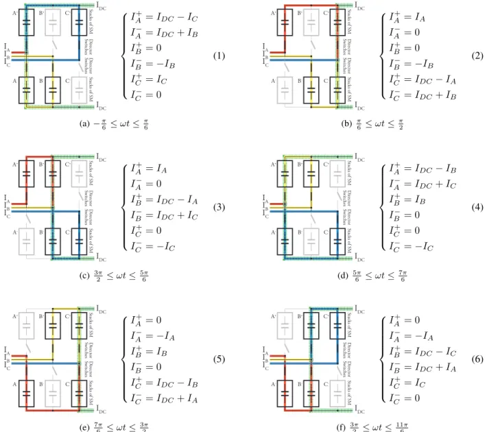
B. Conduction States
The EO-AAC has very different modes of operation
com-pared to the SO-AAC. With an overlap period of 60◦ there
are six different arm conduction states, as illustrated in Fig. 2, and in each conduction state there are exactly four arms conducting, two top arms and two bottom arms, with one top and one bottom arm in the same phase (thus being in overlap mode). The currents flowing in the six arms for each of the six conduction states are noted in (1)-(6) within Fig. 2. The fact that there is always one phase with both of its arms conducting is important because there is therefore always a path for DC current (the dashed green path in Fig. 2) to circulate through a pair of arms resulting in the DC link current being independent from the rectification of AC phase currents. Examining the three AC phase currents (the solid red, yellow, blue paths in Fig. 2) in each state it can be seen that they meet at the midpoint of the arms of the phase that is in overlap and therefore, at this point, they sum to zero and do not circulate through the DC link.
These two features of the 60◦ extended overlap mode of
operation are important. The fact that the three AC currents
meet and cancel within the converter, and not in the DC link as was the case for the SO-AAC, means that the DC current waveform does not include the 6-pulse ripple arising from direct rectification by the simple alternation of the arm conduction periods, which in turn means that there is no need for a DC-side filtering capacitor to provide a low impedance path to the 6-pulse ripple. The fact that there is always a path for DC current through a pair of arms, not just for short periods as in the SO-AAC, means that the AC and DC side powers can be balanced, regardless of the AC to DC voltage ratio. This results in the elimination of the energy balancing sweet-spot limitation that was inherent to the SO-AAC.
C. AC Voltage Magnitude
The natural energy balance provided by the sweet-spot of the SO-AAC tied the converter to operating close to one AC voltage magnitude that was a certain ratio of the DC voltage. The EO-AAC is freed from this constraint and fresh optimization of the AC voltage magnitude can be undertaken. The changes of conduction path inherent to AAC operation (through the action of the DS) can lead to abrupt changes in the arm currents. It is possible to choose an AC voltage magnitude that reduces or eliminates sharp transitions in the arm current waveforms and thus eases the burden on the current regulators. Note that even when the arm currents have sharp transitions, the phase currents and DC current remain smooth.
The approach adopted here is that, by equating the arm current equations (1)-(6) at their respective period boundaries, a pair of alternative conditions for smooth arm currents can be obtained (10) and (11). To illustrate this, the change in current equation of the upper arm in phase A when the transition from
State (1) to State (2) is made atωt= π
6 is taken as an example: (1) :IA+ (π 6 ) =IDC−IˆACsin ( 5π 6 + ΦAC ) (2) :IA+ (π 6 ) = ˆIACsin (π 6 + ΦAC ) (7)
The current magnitudes in (7) can be substituted by the voltage magnitudes by using the definition of active power (8) so that the condition for smooth arm current waveform can be expressed as (9). P = 3 2 ˆ VACIˆAC cos (ΦAC) =VDCIDC (8) 3 ˆVAC cos (ΦAC) = 2VDC cos (ΦAC) (9)
There are two possible solutions for (9). The first solu-tion (10) indicates that if the peak AC phase voltage is equal to two-thirds of the DC bus voltage magnitude, then the mix of DC and AC currents in the arm current (under constant power flow conditions) will lead to smooth transitions into or out of the overlap period. The second solution (11) states that, regardless of the AC to DC voltage ratio, the arm current will always be smooth if only reactive power is generated by the converter (i.e. no active power).
I A I B I C IDC I DC S tacks o f SM S tacks o f SM D ir ecto r S w itches D ir ecto r S w itches A+ B+ C+ A- B- C - IA+=IDC−IC IA− =IDC+IB IB+= 0 IB− =−IB IC+=IC IC− = 0 (1) (a)−π 6 ≤ωt≤ π 6 I A I B I C IDC I DC S tacks o f SM S tacks o f SM D ir ecto r S w itches D ir ecto r S w itches A+ B+ C+ A- B- C - IA+ =IA IA− = 0 IB+ = 0 IB− =−IB IC+ =IDC−IA IC− =IDC+IB (2) (b) π 6 ≤ωt≤ π 2 IA IB IC I DC IDC S tacks o f SM S tacks o f SM D ir ecto r S w itches D ir ecto r S w itches A+ B+ C+ A- B- C - IA+=IA IA−= 0 IB+=IDC−IA IB−=IDC+IC IC+= 0 IC−=−IC (3) (c) 32π ≤ωt≤ 56π IA IB IC I DC IDC S tacks o f SM S tacks o f SM D ir ecto r S w itches D ir ecto r S w itches A+ B+ C+ A- B- C - IA+ =IDC−IB IA− =IDC+IC IB+ =IB IB− = 0 IC+ = 0 IC− =−IC (4) (d) 56π≤ωt≤76π I A I B I C IDC I DC S tacks o f SM S tacks o f SM D ir ecto r S w itches D ir ecto r S w itches A+ B+ C+ A- B- C - IA+= 0 IA− =−IA IB+=IB IB− = 0 IC+=IDC−IB IC− =IDC+IA (5) (e) 7π 6 ≤ωt≤ 3π 2 I A I B I C IDC I DC S tacks o f SM S tacks o f SM D ir ecto r S w itches D ir ecto r S w itches A+ B+ C+ A- B- C - IA+= 0 IA− =−IA IB+=IDC−IC IB− =IDC+IA IC+=IC IC− = 0 (6) (f) 3π 2 ≤ωt≤ 11π 6
Fig. 2: The six different conduction states of the EO-AAC, showing the current paths and arm current equations.
(9)⇒VˆAC= 2 3VDC (10) or ⇒ΦAC= π 2 +kπ (11)
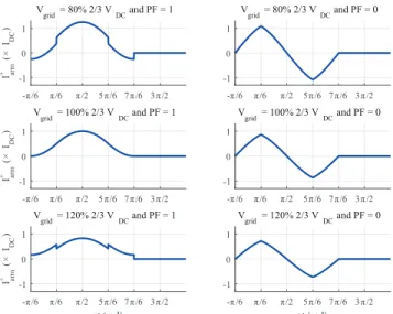
The two conditions (10) and (11) for smooth arm current waveforms are illustrated in Fig. 3 in which the expected arm current waveform (for the upper arm in phase A) is shown for 6 operating conditions: three choices of AC voltage and two choices of power factors. On the left hand side are the results for real power only (unity power factor) and for an AC grid voltage that is 120%, 100% and 80% of the optimal ratio (10) of the DC voltage. Only for the optimal case is the waveform seen to be smooth; at 80% and 120%, the waveform has discontinuities at the boundaries of the conduction states. However, even with a voltage 20% away from the optimal case, the discontinuities are not as pronounced as for the SO-AAC. On the right hand side of Fig. 3 are the results for reactive power only (power factor zero) and here it can be
seen that the waveforms are continuous for all AC voltage magnitudes (although the slope changes abruptly). It can be expected that in general the arm current waveforms will be smoother when reactive power is flowing in addition to real power. A smooth current waveform at the conduction state boundaries is important in easing the burden on the current regulators but also means that the current returns to zero at the end of the arm’s conduction period and thus soft switching of the director switch can be ensured without additional control action. These are good reasons to operate at or close to the optimal voltage ratio.
D. Triplen Harmonic Voltage Injection
Extending the overlap period directly influences the required voltage rating of the SM stacks because they are required to match the AC voltage waveform for longer than half a cycle and therefore for a voltage swing of more than half of the peak-to-peak phase voltage. A means to mitigate this rating increase was suggested in [43] and consists in injecting a
-π /6 π /6 π /2 5 π /6 7 π /6 3 π /2 -1 0 1 Iarm + ( × ID C ) V grid = 80% 2/3 VDC and PF = 1 -π /6 π /6 π /2 5 π /6 7 π /6 3 π /2 -1 0 1 Iarm + ( × ID C ) V grid = 100% 2/3 VDC and PF = 1 -π /6 π /6 π /2 5 π /6 7 π /6 3 π /2 ωt (rad) -1 0 1 Iarm + ( × ID C ) V grid = 120% 2/3 VDC and PF = 1 -π /6 π /6 π /2 5 π /6 7 π /6 3 π /2 -1 0 1 V grid = 80% 2/3 VDC and PF = 0 -π /6 π /6 π /2 5 π /6 7 π /6 3 π /2 -1 0 1 V grid = 100% 2/3 VDC and PF = 0 -π /6 π /6 π /2 5 π /6 7 π /6 3 π /2 ωt (rad) -1 0 1 V grid = 120% 2/3 VDC and PF = 0
Fig. 3: Arm current waveforms for different AC to DC voltage ratios and power factors.
-1 -0.5 0 0.5 1 Voltage ( × V DC ) Voltage ( × V DC ) Voltage ( × V DC ) k3 = 0 -1 -0.5 0 0.5 1 k3 = 0.5 -π /6 π /6 π /2 5 π /6 7 π /6 3 π /2 ωt (rad) -1 -0.5 0 0.5 1 k3 = 1
Converter Stack + Director + Stack - Director
-Fig. 4: Stack of SM and DS voltage waveforms for triplen harmonic injection magnitudes.
specific triplen harmonic voltage. Equation (12) describes this
triplen harmonic voltage, where k3 represents the magnitude
relative to half the peak AC voltage and tri(3t) is a triangle
wave at three times the AC grid frequency.
V3(t) =k3
ˆ VAC
2 tri(3t) (12)
Equation (13) describes the voltage that appears across an arm which is thus split between the SM stack and DS within the arm. VArm+ (t) =VDC 2 −(VAC(t) +V3(t))
VArm+ (t) =VStack+ (t) +VDirector+ (t)
(13)
Figure 4 illustrates the voltages of the SM stacks and
DSs needed to create the arm voltage for k3 = 0, 0.5 and
1.0. With no triplen harmonic, the SM stack must produce
+0.86and−0.27times VDC. Adding the triangle wave term
reduces the peak positive voltage of the stack and increases the negative voltage (making better use of the bipolar capability
of FB SMs within the stacks) until at k3 = 1.0 the use is
symmetric at ±0.5VDC. Another way of looking at this is
that adding the triplen voltage in this fashion has flattened the region of the zero-crossing of the converter voltage and accentuated the peak voltage. This is the opposite sense and effect with which triplen harmonic injection is normally used in power converters. This use of triplen harmonic voltage has the benefits of lowering the voltage rating of the stacks, thus reducing the number of SMs required but it also increases the voltage rating (and number of devices) of the DSs due to the increased value of the peak converter voltage.
The voltage rating of the stacks of SMs and DSs are dictated by two points in the fundamental cycle. The following
example considers the upper arm in phase A (A+) but it
can be reworked for the other arms, using the symmetry of the converter. First, at the end of the overlap period, i.e.
the transition from State (4) to State (5) at ωt = 76π in
Fig. 2, the stack should ideally generate its maximum voltage while the DS voltage is still zero (necessary for zero-current, zero-voltage soft-switching). Second, at the minimum point of the converter voltage waveform, i.e. at the transition from
State (5) to State (6) at ωt = 32π in Fig. 2, arm A+ is not
conducting and the DS has to support the difference between the AC and DC grid voltages minus the contribution from the stack which should be its maximum voltage. Implementing the above factors into (13) leads to the following voltage equations: ˆ VStack= VDC 2 + ˆVAC ( 1 2 − k3 2 ) ˆ VDirector = ˆVAC ( 1 2+k3 ) (14)
At k3 = 1, the converter voltage waveform is flat for the
entire overlap period thus reducing the SM stack voltage rating to its lowest possible value at exactly half the DC bus voltage.
However, under this same condition (k3= 1), the SM stacks
would also be rated at less than the AC peak voltage magnitude which would mean that insufficient SM stack voltage is present to fully control the arm currents with a DC-side short circuit
fault. A better solution lies at k3 = 0.5 where the converter
voltage waveform is only half its usual voltage magnitude during the overlap period. Under this condition, the SM stack voltage rating is exactly equal to the AC grid peak voltage at
the end of the overlap period. Substitutingk3= 0.5in (14) and
using the optimal AC voltage magnitude (10) leads to equal voltage ratings for the SM stack and DS as defined in (15).
ˆ
VStack= ˆVDirector =
2
3VDC (15)
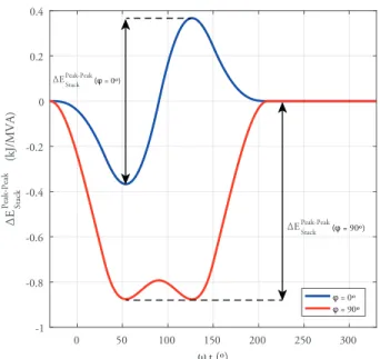
The number of SMs in the stacks and the number of series-connected power modules in the DSs can be found from (15) based on the voltage ratings of a SM and of a single DS power module. E. Capacitor Sizing 0 50 100 150 200 250 300 ω t (º) -1 -0.8 -0.6 -0.4 -0.2 0 0.2 0.4 ∆ E Sta ck Peak -Peak (kJ/MVA ) φ = 0º ∆E Stack Peak-Peak (φ = 0º) φ = 90º ∆E Stack Peak-Peak (φ = 90º)
(a) Energy deviation profile (in kJ/MVA) of one stack in the EO-AAC for two different AC current angles, assuming 50 Hz operation. 10 20 30 40 30 210 60 240 90 270 120 300 150 330 180 0 Inverter Inductive Rec tifie r Capacitive MMC SO-AAC EO-AAC
(b) Total relative energy requirement (in kJ/MVA) in the 6 SM stacks of the EO-AAC and other modular converters, depending
on the AC current phase angle, assuming∆V = 10%and 50 Hz
operation.
Fig. 5: Numerical analysis of the energy deviation and capac-itor sizing in the AAC and MMC.
Like all modular converters, the EO-AAC requires sufficient voltage on the SM capacitors of each stack to maintain control of the arm currents. The SM capacitance has to be chosen large enough to ensure that the voltage deviation over a fundamental cycle caused by conduction of current is within some specified range. In the methodology developed in [7] and summarized in (16), the minimum SM capacitance is obtained by first estimating the peak-to-peak energy deviation for operation
across the region of P + j Q plane that is required and
identifying the worst case. This highest energy deviation is
then combined with the allowed SM voltage deviation (∆V)
to identify the capacitance. ∆EStack(t) = ∫ t 0 VStack(θ)IStack(θ)dθ
EStackN ominal≥ ∆E
P eak−P eak Stack 4 ∆V CSM = 2EN ominal Stack NSMVN ominal 2 SM (16)
Fig. 5b plots the total relative energy requirement for all power factor angles, indicated in total nominal capacitive stored energy across all 6 stacks (in kJ) per units of converted apparent power (in MVA). It is seen that the EO-AAC has a somewhat higher intra-cycle energy deviation than the SO-AAC but both are significantly less than the MMC. Taking a simple case where there is no restriction on power factor angle, the highest value of normalized stack energy deviation of the
EO-AAC is 0.895∥3Sω∥ (this assumed the AC to DC voltage
ratio defined in (10) and triangular triplen harmonic voltage
injection of k3 = 0.5), with ∥S∥ being the apparent power
magnitude. Using this value in (16) with∆V = 0.1leads to a
stored energy specification for the SM capacitance across all
6 stacks of14.25kJ/MVA.
The SM capacitive energy storage of the EO-AAC is greater
than the SO-AAC (10.25kJ/MVA) but it is important to note
that the absence of ripples (6-pulse or otherwise) in the DC current has obviated filtering on the DC side. It was estimated in [7] that a DC bus capacitance equivalent to two additional stacks worth of SM capacitors would be needed with the SO-AAC. Thus it can be said that the EO-AAC requires an equivalent volume of capacitance to the SO-AAC with its DC bus capacitance included, thus conserving the compact design which was one of the attractive characteristics of the SO-AAC. F. Inductive Elements
The stacks of SMs act like voltage sources because of the ability to switch charged capacitors in and out of the conduction path. It is the action of these imposed voltages over the inductors of the AAC, or MMC, that facilitates control of the currents and the size of the inductances plays an important role in control of current flow, e.g. the arm inductors in the MMC [8]. Furthermore, the number of inductors needed is no greater than the number of independent currents in the circuit. The EO-AAC only has four arms in conduction at any time. The two phases with only one arm in conduction have that arm directly in series with the AC-side phase reactor. The phase in overlap mode can have its DC-side current regulated by
DC-side inductors. Since the AC transformer already provides the phase reactor through its leakage inductance, that leaves the EO-AAC only requiring two DC inductors for current control purposes and these only need to be specified for current control purposes since fault-ride through capability is present.
Therefore, the DC-side inductors can be small (e.g.≤0.1 pu).
A reduction in the number of explicit inductors from six in the MMC to two in the EO-ACC, in addition to the small total capacitive energy storage as explained in the Section II-E, could represent a significant space saving if these are all air-cored inductors with large clearance distances from other structures.
G. Control Systems
A complex converter topology such as the EO-AAC requires the support of an extensive control system to ensure proper operation, as detailed in Sections II-B to II-D. The general architecture of the EO-AAC controller is illustrated in Fig. 6. The extensive nature of this controller would require a paper on its own but a summary of its architecture is explained below to give a better context to the operation of the EO-AAC, especially for the experimental results presented in Section III.
Power Management Arm Conduction Controller Reference Creator Director Switch Controller Low Level Controller Current Controller P, Q ref Firing Commands VDC , VAC Energy Management VSM IARM
Fig. 6: Block diagram of the control architecture. Starting with the measurement of the AC and DC voltages, the “Power Management” synchronises the converter to the grids and translates the P-Q demands into AC and DC current references. The “Energy Management” monitors the capacitors voltages of the SMs within the converter, and computes appropriate actions in terms of internal voltage and current adjustments in order to keep the energy level within the stacks close to their nominal value. It operation is closely related to the one of the MMC [44], [45] and SO-AAC [34]. The “Arm Conduction Controller” determines which 4 of the 6 arms of the EO-AAC are conducting, in synchronisation with the AC phase angle. Knowing which arms are in conduction also allows the “Director Switch Controller” to determine the conduction state of the DS, especially the ideal timing to ensure their soft-switching. Using all the above information, the “Reference Creator” [46] computes the current wave-forms which should be flowing through each arm at each controller time step, using a state-space model-based feed-forward supplemented by proportional gains computed through the LQR method. The “Current Controller” compares these reference waveforms with the measured arm currents and computes the optimal stack voltage, similarly to the method described in [47], [48]. Finally, the “Low Level Controller” converts the stack voltage commands into individual SM firing commands, taking into account the state of their respective DS and voltage deviations between the individual SMs using sorting algorithms similar to [49], [50].
III. EXPERIMENTALVALIDATION
A. Experimental Setup
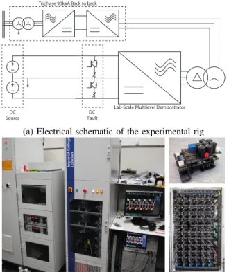
The experimental EO-AAC is a 12 kVA, ±600 V DC
converter with 10 SMs per stack. It was first presented in its prototype form in [51] and upgraded for [52]. The converter is controlled through an OPAL-RT real-time computing system running with a sampling frequency of 10 kHz. The converter is connected to a DC bus consisting of a unidirectional DC power supply, a load bank and a DC-side fault emulator in the form of a low resistance switched across the two DC poles, as shown in Fig. 7. The AC voltage is generated by Triphase inverters which allows the emulation of different grid conditions. Table I lists all the parameters of the experimental setup. The IGBTs in the SMs are however switching at a higher frequency than the grid frequency due the fact that there are only 10 SMs per arm, as opposed to hundreds in an actual HVDC converter. In all the following figures showing experimental data, the following variables have been measured directly using an oscilloscope with high frequency bandwidth in order to capture most of the fast transients: the arm currents, DC currents and stack voltages. All the other variables (AC currents, AC voltage, SM voltages) are recorded by the OPAL-RT system running at the sampling frequency of the controller, the architecture of which is detailed in Section II-G.
Triphase 90kVA Back to back
DC Source
DC Fault
Lab-Scale Multilevel Demonstrator
(a) Electrical schematic of the experimental rig
(b) Converter in its cabinet (left), one full-bridge SM (top-right) and the 6 stacks of series-connected SMs with the DS at the bottom (bottom-right).
Fig. 7: Experimental rig used in this study.
The DC fault apparatus consists of IGBTs in series with
a low impedance resistors (4.7 Ω) connected across the DC
terminals. The firing signals for the IGBTs are generated independently of the converter control system. This imple-mentation was motivated to ensure that the controller has no
prior knowledge to the inception and clearance of a fault. During the initial instance of the fault, the controller has to cope with the fault conditions by itself before the fault detection algorithm establishes the nature of the fault and applies the pre-determined fault response. The detection of the presence or removal of a DC-side fault is based on hysteresis threshold crossing by the DC bus voltage. A fall of the DC bus voltage magnitude below 60% of its nominal magnitude triggers the fault response by the converter which consists, in this experiment, of moving into the STATCOM mode where the active power is dropped to zero and a constant capacitive power at 0.3 pu is provided to the grid. During this period, the DC power supply, which is used to provide power to the DC bus in the test rig, remains in current limit mode set at 12 A. This results in a retained DC voltage of around 120 V (i.e. 0.1 pu). When the fault resistance is disconnected, the DC power supply starts recharging the DC bus. After the DC bus voltage magnitude has remained above 80% for at least one full cycle, the controller considers that the fault is cleared and moves back into recovery mode by ramping the power back up (at a rate of 10 pu/s) up to its pre-fault set point. In a real system it would be feasible for the AAC to recharge the network capacitance, if required, as shown in [52].
Sections III-B to III-C present the results from three tests which illustrate and verify the material presented in Section II. Further experimental results from the EO-AAC were presented in [52] such as power reversal, and both symmetrical and asymmetrical AC faults.
TABLE I: Characteristics of the EO-AAC experiment
Characteristic Symbol Value
Power rating |S| 12 kVA
DC bus voltage VDC ±600 V AC line voltage (RMS) Vline 846 V Nominal SM voltage VSM 90 V Number of SMs per stack NSM 10 SM capacitor CSM 1,000µF
Phase reactor L 24 mH
Arm inductor Larm 1.3 mH
DC inductor LDC 23 mH
DC fault resistor Rf ault 4.7Ω Control sampling frequency FS=T1S 10 kHz
B. Normal Operation
The EO-AAC experimental rig generates the electrical waveforms as described in Section II when operated under normal conditions. Fig. 8 shows the experimental EO-AAC
operating under steady state power flow of P = 1 pu
(12 kW) inverting and no capacitive power. The electrical
waveforms are as described in Section II in that the AC and
DC current waveforms (2nd and 4th plots) are smooth (apart
from some switching noise evident). Operation is close to
VAC= 23VDC (the optimal point defined in (10)) and the arm
currents (6th plot) show the absence of discontinuities at the
conduction state transitions, as discussed in Section II-C. The
0 0.005 0.01 0.015 0.02 0.025 0.03 0.035 0.04 0.045 0.05 -2 0 2 VAC (kV) 0 0.005 0.01 0.015 0.02 0.025 0.03 0.035 0.04 0.045 0.05 -10 0 10 IA,B,C (A ) 0 0.005 0.01 0.015 0.02 0.025 0.03 0.035 0.04 0.045 0.05 -1 0 1 VDC (kV) 0 0.005 0.01 0.015 0.02 0.025 0.03 0.035 0.04 0.045 0.05 0 5 10 I + DC (A ) 0 0.005 0.01 0.015 0.02 0.025 0.03 0.035 0.04 0.045 0.05 -1 0 1 V + (kA V ) 0 0.005 0.01 0.015 0.02 0.025 0.03 0.035 0.04 0.045 0.05 -5 0 5 10 I + (AA ) 0 0.005 0.01 0.015 0.02 0.025 0.03 0.035 0.04 0.045 0.05 Time (s) 80 90 100 VSM (V )
Fig. 8: Experimental results from the hardware converter operating at a set-point of 1 pu P and 0 pu Q. Top-bottom: converter AC line voltages, converter phase currents, DC pole to ground voltages, DC current, phase A upper arm stack voltage, phase A upper arm current, average SM voltage in each stack of SM.
stack voltages (5th plot) show the smaller rate of voltage rise
during the overlap periods and the heightened voltage peak in the middle of the conducting states expected from triplen harmonic voltage injection.
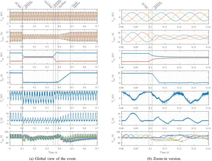
C. DC-Side Fault
The EO-AAC retains the property of the SO-AAC of being able to fully control the arm currents even in the presence of a DC-side short-circuit fault to the extent that it can operate as a STATCOM [34], [38], [39]. Fig. 9 shows the main converter waveforms with a short-circuit applied to the
DC-side at 0.10 s and released at 0.35 s. At the instance of
the fault, the controller maintains the currents close to their references despite the change in operating condition. After the fault detection declares the presence of the DC-side fault, the controller moves to a STATCOM operation by setting the real power reference to zero and a 0.3 pu capacitive reactive power reference. Subplots 2, 4, 6 and 7 from the top of Fig. 9 demonstrate that the arm, phase and DC currents, and SM voltages exhibit only minor deviations from their reference
0 0.1 0.2 0.3 0.4 0.5 0.6 0.7 -2 0 2 VAC (kV) 0 0.1 0.2 0.3 0.4 0.5 0.6 0.7 -10 0 10 IA,B,C (A ) 0 0.1 0.2 0.3 0.4 0.5 0.6 0.7 -1 0 1 VDC (kV) 0 0.1 0.2 0.3 0.4 0.5 0.6 0.7 0 5 10 I + DC (A ) 0 0.1 0.2 0.3 0.4 0.5 0.6 0.7 -1 0 1 V + (kV)A 0 0.1 0.2 0.3 0.4 0.5 0.6 0.7 -5 0 5 10 I + (AA ) 0 0.1 0.2 0.3 0.4 0.5 0.6 0.7 Time (s) 80 90 100 VSM (V ) DC F ault End of F ault Detection (80% Thr eshold) Detection (60% Thr eshold)
Start Ramp NormalOperation
(a) Global view of the event.
0.08 0.09 0.1 0.11 0.12 0.13 0.14 -2 0 2 VAC (kV) 0.08 0.09 0.1 0.11 0.12 0.13 0.14 -10 0 10 IA,B,C (A ) 0.08 0.09 0.1 0.11 0.12 0.13 0.14 -1 0 1 VDC (kV) 0.08 0.09 0.1 0.11 0.12 0.13 0.14 0 5 10 I + DC (A ) 0.08 0.09 0.1 0.11 0.12 0.13 0.14 -1 0 1 V + (kV)A 0.08 0.09 0.1 0.11 0.12 0.13 0.14 -5 0 5 10 I + (AA ) 0.08 0.09 0.1 0.11 0.12 0.13 0.14 Time (s) 80 90 100 VSM (V ) DC F ault Detection (60% Thr eshold) (b) Zoom-in version.
Fig. 9: Experimental results showing the DC-side fault blocking and STATCOM capabilities of the EO-AAC, followed by the restoration of the DC bus voltage by the converter and back to normal operation. The format is the same as in Fig. 8.
waveforms through the fault inception and clearance. There is a small amount of retained voltage (about 120V) when the DC fault is active due to the DC power supply in current limiting mode at around 12A still connected to the DC bus. This retained DC voltage does not impact the capability of the converter to maintain current control, as in the case of a 0 V DC bus voltage. When the fault is cleared, the DC bus voltage can rise under the control of the DC power supply. Once the detection algorithm concludes that the fault is cleared (i.e. DC bus voltage above 80% nominal value for at least one full cycle), the converter resumes normal operation by transitioning through a power ramp of at a rate of 10 pu/s.
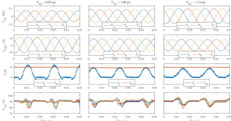
D. AC Voltage Magnitude Variation
In order to demonstrate the ability of the EO-AAC to operate across a wider range of AC/DC voltage ratios (in other words, freedom from the restrictions of the SO-AAC sweet-spot), the experimental converter was subjected to steps in the AC voltage magnitude, generated by the Triphase inverters. Each column in Fig. 10 shows a different AC voltage magnitude, with one operating point below the optimal voltage ratio and one above. The EO-AAC is seen to adapt and operates stably
in each case. When operated away from the optimal point (10), the arm current waveforms (but not the phase currents) start to show discontinuities when the arms move from one conduction state to another, similar to Fig. 3. The amplitude of these discontinuities can be predicted in relation to the nominal DC current magnitude, as stated in (17), by noting the variation of the AC voltage magnitude around its optimal point (10) by
the factor kAC and the per unit amount of power kS going
through the converter. ∆I=I + A (π 6 +)−I+ A (π 6− ) IN om DC =kS ( 1− 1 kAC ) cos (ΦAC) (17)
However, the magnitude of these discontinuities remains small, especially compared to those observed in the SO-AAC. The discontinuities are approximately 18% of the DC current magnitude in the case of an AC voltage magnitude
of 0.85 pu and unity power factor. As noted in Section II-C
and demonstrated in (17), operation at unity power factor corresponds to the worst case scenario and the generation of reactive power reduces the magnitude of these arm current
discontinuities.
Finally, the voltage rating of the stacks in the EO-AAC has a small dependance to the AC voltage magnitude variation. This
is proven by (18) resulting from (14) with k3 = 0.5, where
kACmeasures the AC voltage magnitude’s relative variation to
its nominal value (10). This results in a voltage rating increase
of the stacks of SMs by ±2.5% for an AC voltage magnitude
variation of ±15%. ˆ VAC=kAC 2 3VDC ˆ VStack= VDC 2 ( 1 2 − kAC 6 ) (18) IV. DISCUSSION
The EO-AAC should be compared against its predeces-sor, the SO-AAC [34] and the incumbent technology, the MMC [4]. The Half-Bridge MMC (HB-MMC) is normally the preferred format because of its low power losses but the comparison here will also include the Hybrid-MMC (H-MMC) because it has DC fault ride-through capability that makes it a competitor to the AAC. Here the H-MMC is taken to have the same number of SMs as the HB-MMC but with half of them replaced by full-bridge SMs [16]. This format of the
H-MMC only allows under-modulation (i.e. VˆAC ≤ 12VDC) but
does allow continued current control with a short-circuited DC link. Note that the SO- and EO-AAC are both configured to over-modulate and have higher nominal AC voltages than the MMC of the same DC voltage, as defined by the sweet-spot and the optimal operating point (10) respectively.
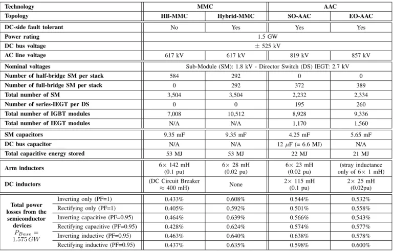
These four converter types are compared in Table II when
configured as a ±525 kV, 1.5 GW converter. The SMs have
been rated at 1.8 kV in order to use the 3.3 kV - 1.5 kA IGBT module (Infineon FZ1500R33HL3) at a voltage de-rating factor of 60% when allowing the SM voltage to
fluc-tuate by ±10%. For the DS, 4.5 kV - 1.5 kA Press-Pack
IEGTs (Toshiba ST1500GXH24) are used because of their tendency to fail short circuit; a desired behaviour for series-connected power devices. Applying the same de-rating factor (and ignoring the SM voltage deviation margin) leads to a voltage rating of 2.7 kV per IEGT. The SM capacitors were sized as described in Section II-E. The arm inductors in the HB-MMC were sized at 0.1 pu to limit the rate of rise of the current in case of a DC-side fault, as detailed in [8]. In the case of the H-MMC, this current limiting criteria no longer applies, thus the arm inductors have been reduced to 0.02 pu to achieve a good balance between control margins and inductor size, also in line with other works related to the H-MMC found in the literature [8], [16], [17]. Power losses in the semiconductors were assessed by running a time-domain simulation in Simulink, then calculating the voltage drops across all the IGBTs, IEGTs and internal diodes using polynomial approximations to the datasheet curves for the conduction losses and switching power losses added at each event, following the procedure detailed in [53], [54] and also used in [16].
The total number of SMs in the AAC is less than the MMC because the SM stacks need only to generate a lower peak
voltage while the arm is conducting, with the DS supporting the additional voltage when the arm is not conducting. Overall, the number of semiconductor devices in the EO-AAC is about 8% higher than the SO-AAC, 4% higher than the H-MMC also and 55% higher than the HB-H-MMC. This has implications for cost but for size and power losses there are other important factors to consider. Each AAC SM uses a smaller capacitor than the MMC SM (approximately half) and the AAC uses fewer SMs (approximately two-thirds) and so the stored capacitive energy and physical volume they occupy is smaller. The EO-AAC has the lowest number of explicit inductors (two) because it can use the leakage of the interface transformer and does not require arm inductors. The total size of the inductors is influenced by their number as well as stored energy because of clearance and shielding issues. The HB-MMC, being the only converter of the four unable to control arm currents during a DC-side short-circuit would need significant inductance somewhere (in the arms or DC link) to limit the rise of fault currents. The SO-AAC is the only one of the four to not provide inherently smooth DC current and therefore must include a large capacitance on the DC link.
The power efficiency results for six operating points are shown at the bottom of Table II. As expected, the H-MMC has higher losses than the HB-MMC because it has more semiconductor devices in the conduction paths for the same pattern of currents. The SO- and EO-AAC have broadly similar numbers of IGBTs overall but they are put to different use. Nonetheless, the losses in the EO-AAC are similar and a little bit less than the H-MMC (by about -9%). It is important to note that these losses are for only the semiconductor devices and other substantial losses in the transformer, inductors and cooling system need to be considered in a complete converter station [55].
In summary, all the DC fault ride-through converters here suffer a power loss penalty compared to the HB-MMC. The EO-AAC has solved the two major drawbacks of the SO-AAC: it is not tied to a sweet-spot and it does not need a DC-side filtering capacitor (a significant volume saving). The EO-AAC and H-MMC are similar in terms of controllability in normal and abnormal conditions, and in terms of power loss. The EO-AAC requires approximately half the volume of SM capacitance and 2 rather than 6 explicit inductors, contributing to a more compact design of the converter station.
V. CONCLUSION
The Extended Overlap Alternate Arm Converter (EO-AAC) is an improved version of the previously proposed Alternate Arm Converter which was operated with a Short Overlap (SO-AAC). Some of the advantages of the EO-AAC stem from its operating mode but there are also some from consequential changes in the circuit itself such as the removal of the DC-side filtering capacitor and reduction in the number of inductors.
The new mode of operation employs an overlap of 60◦ in the
conduction of top and bottom arms whereas previously the
SO-AAC used an overlap of about 10◦ as an opportunity to
circulate a balancing current between the arms and the DC link. The new operating mode ensures that there is always a
0 0.01 0.02 0.03 0.04 0.05 -1.5 0 1.5 VAC (kV) V AC = 0.85 pu VA VB VC 0 0.01 0.02 0.03 0.04 0.05 -10 0 10 IA,B,C (A) IA IB IC 0 0.01 0.02 0.03 0.04 0.05 0 10 I (A) I+A IDC 0 0.01 0.02 0.03 0.04 0.05 70 80 90 100 VSM (V) 0 0.01 0.02 0.03 0.04 0.05 V AC = 1.00 pu VA VB VC 0 0.01 0.02 0.03 0.04 0.05 IA IB IC 0 0.01 0.02 0.03 0.04 0.05 I+A IDC 0 0.01 0.02 0.03 0.04 0.05 0 0.01 0.02 0.03 0.04 0.05 V AC = 1.15 pu VA VB VC 0 0.01 0.02 0.03 0.04 0.05 IA IB IC 0 0.01 0.02 0.03 0.04 0.05 I+A IDC 0 0.01 0.02 0.03 0.04 0.05 Time (s) Time (s) Time (s)
Fig. 10: Experimental results of the EO-AAC operation under a wide range (±15%) of AC voltage magnitude variations.
path to circulate current between the DC side and the converter independent of the AC-side currents. It also means that the AC currents sum to zero within the converter phase that is in overlap and do not flow via the DC link. The EO-AAC has been shown to have these benefits over the SO-AAC: (i) smooth DC current waveform thus removing the need for a bulky low-frequency DC filtering capacitor, compensated by a small increase in the total capacitive energy storage in the SM but remains smaller than that of the MMC, (ii) release from the sweet-spot operating area for energy balancing reasons thus allowing the EO-AAC to operate at any AC to DC voltage ratio. It has also been shown that an optimal operating point
exists at VˆAC = 23VDC where there are no discontinuities in
the arm current waveforms between the different conduction periods leading to a further benefit which is (iii) the easing of the current control task and soft-switching of the director switches.
The EO-AAC retains the benefits of the original SO-AAC, namely (iv) DC fault ride-through capability (and a subsidiary benefit of not needing to size inductors for fault current limiting), (v) STATCOM mode of operation during a DC bus outage for additional AC grid support, (vi) the relatively
small capacitive energy storage requirement (14.25kJ/MVA),
(vii) reduced number of inductors (two DC-side inductors as opposed to six arm inductors). The EO-AAC requires more semiconductor devices than the SO-AAC (+8%) and H-MMC (+4%) but this increase has been mitigated by the use of a triangular triplen harmonic voltage injection technique. Comparing these three converter topologies (which are all capable of DC fault ride-through), the power losses in the
semiconductors are broadly similar at approximately0.6% and
above the HB-MMC at 0.43%.
A comparison between the HB-MMC and EO-AAC tech-nologies has identified two key facts. On the one hand, from a purely electrical point of view, the DC-side fault blocking capability comes at a premium of more semiconductor devices (+55%) and higher semiconductor power losses (+30%). On the other hand, from a converter station design point of view, the AAC technology reduces the bulk of several items: fewer submodules (-33%), smaller submodule capacitors (-50%) and fewer inductors (2 instead of 6) when compared to the MMC. All these facts combined mean that the premium usually associated with the DC-fault blocking capability of a VSC could now be offset by the smaller footprint of the converter station, thanks to the EO-AAC technology.
ACKNOWLEDGMENT
The authors gratefully acknowledge the financial support provided by the UK Power Electronic Centre: Converter Theme (ESPRC grant EP/K035096/1), HubNet Consortium (EPSRC grant EP/I013636/1), RESTORES (EPSRC grant EP/L014351/1), EDF Energy R&D UK and the cooperation of GE’s Grid Solutions, including the use of control algorithms for these tests which were developed on their behalf. There are no data sets associated with this publication to report.
REFERENCES
[1] British-Standard-Institution,Terminology for voltage-sourced converters for high-voltage direct current systems, 2014, bS EN 62747:2014. [2] N. Ahmed, A. Haider, D. Van Hertem, L. Zhang, and H.-P. Nee,
“Prospects and challenges of future hvdc supergrids with modular multilevel converters,” in Power Electronics and Applications (EPE 2011), Proceedings of the 2011-14th European Conference on. IEEE, 2011, pp. 1–10.
[3] M. Barnes, D. Van Hertem, S. P. Teeuwsen, and M. Callavik, “Hvdc systems in smart grids,”Proceedings of the IEEE, 2017.
TABLE II: Modular Converter Characteristics
Technology MMC AAC
Topology HB-MMC Hybrid-MMC SO-AAC EO-AAC
DC-side fault tolerant No Yes Yes Yes
Power rating 1.5 GW
DC bus voltage ±525 kV
AC line voltage 617 kV 617 kV 819 kV 857 kV
Nominal voltages Sub-Module (SM): 1.8 kV - Director Switch (DS) IEGT: 2.7 kV
Number of half-bridge SM per stack 584 292 0 0
Number of full-bridge SM per stack 0 292 372 389
Total number of SM 3,504 3,504 2,232 2,334
Number of series-IEGT per DS 0 0 195 260
Total number of IGBT modules 7,008 10,512 8,928 9,336
Total number of IEGT modules N/A N/A 1,170 1,560
SM capacitors 9.35 mF 9.35 mF 4.25 mF 5.65 mF
DC bus capacitor N/A N/A 12µF (= 6.6 MJ) N/A
Total capacitive energy stored 53 MJ 53 MJ 22 MJ 21 MJ
Arm inductors 6×142 mH (0.1 pu) 6×28 mH (0.02 pu) 6×23 mH (0.02 pu) (stray inductance only of 6×1 mH)
DC inductors (DC Circuit Breaker
≈400 mH) None 2×115 mH (0.1 pu) 2×25 mH (0.02pu) Inverting only (PF=1) 0.433% 0.608% 0.544% 0.532% Rectifying only (PF=1) 0.405% 0.592% 0.501% 0.558% Inverting capacitive (PF=0.95) 0.464% 0.639% 0.566% 0.543% Rectifying capacitive (PF=0.95) 0.428% 0.624% 0.574% 0.577% Inverting inductive (PF=0.95) 0.463% 0.640% 0.638% 0.578% Total power
losses from the semiconductor
devices PBase=
1.575GW
Rectifying inductive (PF=0.95) 0.437% 0.635% 0.598% 0.600%
[4] A. Lesnicar and R. Marquardt, “An innovative modular multilevel converter topology suitable for a wide power range,” in Power Tech Conference Proceedings, 2003 IEEE Bologna, vol. 3, Jun. 2003. [5] K. Ilves, S. Norrga, L. Harnefors, and H.-P. Nee, “On energy storage
requirements in modular multilevel converters,”Power Electronics, IEEE Transactions on, vol. 29, no. 1, pp. 77–88, Jan. 2014.
[6] M. Merlin, T. Green, P. Mitcheson, F. Moreno, K. Dyke, and D. Trainer, “Cell capacitor sizing in modular multilevel converters and hybrid topologies,” in Power Electronics and Applications (EPE’14-ECCE Europe), 2014 16th European Conference on, Aug. 2014, pp. 1–10.
[7] M. M. Merlin and T. C. Green, “Cell capacitor sizing in multilevel converters: cases of the modular multilevel converter and alternate arm converter,”IET Power Electronics, vol. 8, no. 3, pp. 350–360, 2015. [8] Q. Tu, Z. Xu, H. Huang, and J. Zhang, “Parameter design principle of
the arm inductor in modular multilevel converter based hvdc,” inPower System Technology (POWERCON), 2010 International Conference on, 2010, pp. 1–6.
[9] L. Tang and B.-T. Ooi, “Locating and isolating dc faults in multi-terminal dc systems,”IEEE Transactions on Power Delivery, vol. 22, no. 3, pp. 1877–1884, 2007.
[10] C. Franck, “Hvdc circuit breakers: A review identifying future research needs,”Power Delivery, IEEE Transactions on, vol. 26, no. 2, pp. 998– 1007, Apr. 2011.
[11] Y. Wang and R. Marquardt, “Future hvdc-grids employing modular multilevel converters and hybrid dc-breakers,” inPower Electronics and Applications (EPE), 2013 15th European Conference on. IEEE, 2013, pp. 1–8.
[12] J. Hafner and B. Jacobson, “Proactive hybrid hvdc breakers - a key innovation for reliable hvdc grids,” inCigre - Bologna Conference, 2011. [13] M. M. Khorassani, “Hybrid dc circuit breaking device,” Dec. 2012, uS
Patent App. 14/367,991.
[14] O. Cwikowski, A. Wood, A. Miller, M. Barnes, and R. Shuttleworth, “Operating dc circuit breakers with mmc,”IEEE Transactions on Power Delivery, 2017.
[15] R. Zeng, L. Xu, and L. Yao, “An improved modular multilevel converter
with dc fault blocking capability,” inPES General Meeting— Conference & Exposition, 2014 IEEE. IEEE, 2014, pp. 1–5.
[16] R. Zeng, L. Xu, L. Yao, and B. W. Williams, “Design and operation of a hybrid modular multilevel converter,”IEEE Transactions on Power Electronics, vol. 30, no. 3, pp. 1137–1146, 2015.
[17] J. Qin, M. Saeedifard, A. Rockhill, and R. Zhou, “Hybrid design of modular multilevel converters for hvdc systems based on various submodule circuits,” Power Delivery, IEEE Transactions on, vol. 30, no. 1, pp. 385–394, Feb. 2015.
[18] R. Li, J. E. Fletcher, L. Xu, D. Holliday, and B. W. Williams, “A hybrid modular multilevel converter with novel three-level cells for dc fault blocking capability,” IEEE Transactions on Power Delivery, vol. 30, no. 4, pp. 2017–2026, 2015.
[19] S. Cui and S.-K. Sul, “A comprehensive dc short-circuit fault ride through strategy of hybrid modular multilevel converters (mmcs) for overhead line transmission,”IEEE Transactions on Power Electronics, vol. 31, no. 11, pp. 7780–7796, 2016.
[20] W. Lin, D. Jovcic, S. Nguefeu, and H. Saad, “Full-bridge mmc converter optimal design to hvdc operational requirements,”IEEE Transactions on Power Delivery, vol. 31, no. 3, pp. 1342–1350, 2016.
[21] R. Marquardt, “Modular multilevel converter: An universal concept for hvdc-networks and extended dc-bus-applications,” inPower Electronics Conference (IPEC), 2010 International, Jun. 2010, pp. 502–507. [22] R. Marquardt, “Modular Multilevel Converter topologies with DC-Short
circuit current limitation,” inPower Electronics and ECCE Asia (ICPE ECCE), 2011 IEEE 8th International Conference on, Jun. 2011, pp. 1425–1431.
[23] T. Modeer, H.-P. Nee, and S. Norrga, “Loss comparison of different sub-module implementations for modular multilevel converters in hvdc applications,”EPE Journal, vol. 22, no. 3, pp. 32–38, 2012.
[24] X. Yu, Y. Wei, and Q. Jiang, “Statcom operation scheme of the cdsm-mmc during a pole-to-pole dc fault,” IEEE Transactions on Power Delivery, vol. 31, no. 3, pp. 1150–1159, 2016.
[25] M. Pereira, “Submodule for a multi-stage power converter having additional energy storage device,” Nov. 4 2010, wO Patent App.
PCT/EP2009/003,352. [Online]. Available: https://www.google.co.uk/ patents/WO2010124706A1?cl=en
[26] K. ILVES, “Three-level submodule for a voltage source converter,” Jan. 9 2014, wO Patent App. PCT/EP2012/063,106. [Online]. Available: https://www.google.co.uk/patents/WO2014005634A1?cl=en
[27] M. Perez, S. Bernet, J. Rodriguez, S. Kouro, and R. Lizana, “Circuit topologies, modeling, control schemes, and applications of modular multilevel converters,”Power Electronics, IEEE Transactions on, vol. 30, no. 1, pp. 4–17, Jan. 2015.
[28] D. Trainer, C. Davidson, C. Oates, N. Macleod, D. Critchley, and R. Crookes, “A new hybrid voltage-sourced converter for hvdc power transmission,” inCigre Session, 2010.
[29] C. Davidson and D. Trainer, “Innovative concepts for hybrid multi-level converters for hvdc power transmission,” inAC and DC Power Transmission, 2010. ACDC. 9th IET International Conference on, Oct. 2010, pp. 1–5.
[30] R. Feldman, M. Tomasini, J. Clare, P. Wheeler, D. Trainer, and R. White-house, “A hybrid voltage source converter arrangement for hvdc power transmission and reactive power compensation,” inPower Electronics, Machines and Drives (PEMD 2010), 5th IET International Conference on. IET, 2010, pp. 1–6.
[31] R. Feldman, M. Tomasini, E. Amankwah, J. C. Clare, P. W. Wheeler, D. R. Trainer, and R. S. Whitehouse, “A hybrid modular multilevel voltage source converter for hvdc power transmission,”Industry Appli-cations, IEEE Transactions on, vol. 49, no. 4, pp. 1577–1588, 2013. [32] G. Adam, S. Finney, B. Williams, D. Trainer, C. Oates, and D.
Critchley, “Network fault tolerant voltage-source-converters for high-voltage applications,” inAC and DC Power Transmission, 2010. ACDC. 9th IET International Conference on, 2010, pp. 1–5.
[33] M. Merlin, T. Green, P. Mitcheson, D. Trainer, D. Critchley, and R. Crookes, “A new hybrid multi-level voltage-source converter with dc fault blocking capability,” inAC and DC Power Transmission, 2010. ACDC. 9th IET International Conference on, Oct. 2010.
[34] M. Merlin, T. Green, P. Mitcheson, D. Trainer, R. Critchley, W. Crookes, and F. Hassan, “The alternate arm converter: A new hybrid multilevel converter with dc-fault blocking capability,” Power Delivery, IEEE Transactions on, vol. 29, no. 1, pp. 310–317, Feb. 2014.
[35] A. Nami, J. Liang, F. Dijkhuizen, and G. Demetriades, “Modular multilevel converters for hvdc applications: Review on converter cells and functionalities,”Power Electronics, IEEE Transactions on, vol. 30, no. 1, pp. 18–36, Jan. 2015.
[36] H. R. Wickramasinghe, G. Konstantinou, and J. Pou, “Comparison of bipolar sub-modules for the alternate arm converter,”Electric Power Systems Research, vol. 146, pp. 115–123, 2017.
[37] G. Tang, Z. Xu, and Y. Zhou, “Impacts of three mmc-hvdc configurations on ac system stability under dc line faults,” Power Systems, IEEE Transactions on, vol. 29, no. 6, pp. 3030–3040, Nov. 2014.
[38] R. Feldman, A. J. Watson, J. C. Clare, P. W. Wheeler, D. R. Trainer, and R. W. Crookes, “DC fault ride-through capability and statcom operation of a hybrid voltage source converter arrangement for HVDC power transmission and reactive power compensation,” inPower Electronics, Machines and Drives (PEMD 2012), 6th IET International Conference on, Mar. 2012, pp. 1–5.
[39] R. Feldman, E. Farr, A. J. Watson, J. C. Clare, P. W. Wheeler, D. R. Trainer, and R. W. Crookes, “Dc fault ride-through capability and statcom operation of a hvdc hybrid voltage source converter,” IET Generation, Transmission & Distribution, vol. 8, no. 1, pp. 114–120, 2014.
[40] J. Ainsworth, M. Davies, P. Fitz, K. Owen, and D. Trainer, “Static var compensator (statcom) based on single-phase chain circuit converters,” Generation, Transmission and Distribution, IEE Proceedings-, vol. 145, no. 4, pp. 381 –386, Jul. 1998.
[41] K. Sharifabadi, L. Harnefors, H.-P. Nee, R. Teodorescu, and S. Norrga, Design, Control and Application of Modular Multilevel Converters for HVDC Transmission Systems. John Wiley & Sons, 2016.
[42] D. R. Trainer, “Converter,” Jun. 2011, uS Patent App. 14/129,923. [43] F. Moreno, M. Merlin, D. Trainer, T. Green, and K. J. Dyke, “Zero
phase sequence voltage injection for the alternate arm converter,” in AC and DC Power Transmission, 2015. ACDC. 11th IET International Conference on, Feb. 2015.
[44] P. Munch, D. Gorges, M. Izak, and S. Liu, “Integrated current control, energy control and energy balancing of modular multilevel converters,” inIECON 2010 - 36th Annual Conference on IEEE Industrial Electron-ics Society, Nov. 2010, pp. 150–155.
[45] P. Delarue, F. Gruson, and X. Guillaud, “Energetic macroscopic repre-sentation and inversion based control of a modular multilevel converter,”
in Power Electronics and Applications (EPE), 2013 15th European Conference on. IEEE, 2013, pp. 1–10.
[46] S. Fekriasl, M. Merlin, T. Green, K. Dyke, F. M. Munoz, O. Jasim, and B. Masoud, “Improvements in or relating to the control of converters,” European Patent EP2884653, 2015.
[47] P. M¨unch, S. Liu, and M. Dommaschk, “Modeling and current control of modular multilevel converters considering actuator and sensor delays,” inIndustrial Electronics, 2009. IECON’09. 35th Annual Conference of IEEE. IEEE, 2009, pp. 1633–1638.
[48] M. M. Belhaouane, F. Colas, F. Gruson, N. B. Braiek, and X. Guillaud, “Control of mmc converter integrated in hvdc link based on quadratic optimization approach,” inControl and Modeling for Power Electronics (COMPEL), 2016 IEEE 17th Workshop on. IEEE, 2016, pp. 1–7. [49] P. M. Meshram and V. B. Borghate, “A simplified nearest level control
(nlc) voltage balancing method for modular multilevel converter (mmc),” IEEE Transactions on Power Electronics, vol. 30, no. 1, pp. 450–462, 2015.
[50] K. Ilves, L. Harnefors, S. Norrga, and H.-P. Nee, “Predictive sorting algorithm for modular multilevel converters minimizing the spread in the submodule capacitor voltages,” IEEE Transactions on Power Electronics, vol. 30, no. 1, pp. 440–449, 2015.
[51] P. Clemow, P. Judge, G. Chaffey, M. Merlin, T. Luth, and T. C. Green, “Lab-scale experimental multilevel modular hvdc converter with temperature controlled cells,” in Power Electronics and Applications (EPE’14-ECCE Europe), 2014 16th European Conference on, Aug. 2014, pp. 1–10.
[52] P. Judge, G. Chaffey, P. Clemow, M. Merlin, and T. Green, “Hardware testing of the alternate arm converter operating in its extended overlap mode,” inCigre HVDC 2015, Seoul, Korea. Cigre, 2015.
[53] British-Standard-Institution,Power losses in voltage sourced converter (VSC) valves for high-voltage direct current systems. Part 1: General requirements, 2014, bS EN 62751-1:2014.
[54] British-Standard-Institution,Power losses in voltage sourced converter (VSC) valves for high-voltage direct current systems. Part 2: modular multilevel converters, 2014, bS EN 62751-2:2014.
[55] B. Jacobson, P. Karlsson, G. Asplund, L. Harnefors, and T. Jonsson, “Vsc-hvdc transmission with cascaded two-level converters,” inCigr´e session, 2010, pp. 1–8.