N A N O E X P R E S S
Open Access
Fabrication of nanowire network AAO and its
application in SERS
Qi Jiwei, Li Yudong, Yang Ming, Wu Qiang, Chen Zongqiang, Peng Jingyang, Liu Yue, Wang Wudeng, Yu Xuanyi,
Sun Qian
*and Xu Jingjun
*Abstract
In this paper, nanowire network anodized aluminum oxide (AAO) was fabricated by just adding a simple film-eroding process after the production of porous AAO. After depositing 50 nm of Au onto the surface, nanowire network AAO can be used as ultrasensitive and high reproducibility surface-enhanced Raman scattering (SERS) substrate. The average Raman enhancement factor of the nanowire network AAO SERS substrate can reach 5.93 × 10⁶, which is about 14% larger than that of commercial Klarite® substrates. Simultaneously, the relative standard deviations in the SERS intensities are limited to approximately 7%. All of the results indicate that our large-area low-cost high-performance nanowire structure AAO SERS substrates have a great advantage in chemical/biological sensing applications.
Keywords:Surface-enhanced Raman scattering; AAO; Nanowire network
Background
Surface-enhanced Raman scattering (SERS) as a power-ful and sensitive technique for the detection of chemical and biological agents received more attention since single-molecule detection with SERS was confirmed [1,2]. The enhancement of Raman signal was mainly at-tributed to the electromagnetic enhancement on the metal surface which was induced by the surface plasmon resonance (SPR). To obtain the huge Raman enhance-ment, noble metal nanogap structures, especially of sub-10-nm gap structures, have attracted considerable scholarly attention, which can support strong SERS due to the existence of enormous electromagnetic enhance-ment in the gap of metal nanostructure [3-16]. The enormous electromagnetic enhancement in the gap of metal nanostructure is caused by the strong coupling of the SPR, which is called ‘hot spot’. Apart from having a huge Raman enhancement, the high-performance SERS substrates should also be uniform and reproducible. Taking into account the commercial application, the high-performance SERS substrates should also be low cost and should achieve high output. Fabrication of high-performance SERS substrates has been the focus of
attention [3-16]. Many low-cost methods and techniques have been proposed, like self-assembly [17,18], indentation lithography [6,19-24], corroding ultrathin layer [25], and femtosecond laser fabrication [26-29]. However, to date, for the existence of many limits for these low-cost tech-niques, the fabrication of large-area high-performance SERS substrate with sub-10-nm gap size is still critical for the practical applications of SERS.
Porous anodized aluminum oxide (AAO) was widely used in the SERS substrate fabrication for the existence of large-area high-ordered array of nanopores and the simple production process. Porous AAO can be used directly as SERS substrate after depositing Au or Ag on the surface [30] and can also be used as template to fabri-cate ordered array nanostructure SERS substrate [31-36]. Previous studies have shown that nanorod array and nano-wire network, with dense nanojunctions and nanogaps, can support stronger SERS than porous structures [37-41]. The question, whether the nanorod array and nanowire network structure can be fabricated just by mak-ing a simple change to the production process of porous AAO, has not attracted the researcher's attention.
In this work, a simple film-eroding process was added after the production process of porous AAO to fabricate large-area low-cost nanowire network AAO which can be used as high-performance SERS substrate after de-positing 50 nm of Au onto its surface. The Raman * Correspondence:[email protected];[email protected]
The MOE Key Laboratory of Weak-Light Nonlinear Photonics, Tianjin Key Laboratory of Photonics and Technology, TEDA Applied Physics School and School of Physics, Nankai University, Tianjin 300457, China
spectra of benzene thiol on the nanowire network AAO SERS substrates are measured and the average Raman enhancement factors (EFs) are calculated. Comparing with the porous AAO SERS substrates, the Raman peak intensities and the average EFs of nanowire network AAO SERS substrates have a significant enhancement. The average EF of our sensitive SERS substrate can reach 5.93 × 10⁶, about 35 times larger than that of por-ous AAO SERS substrate and about 14% larger than that of Klarite® substrates (Renishaw Diagnostics, Glasgow, UK), which indicates an enormous electromagnetic enhancement that exists in the nanowire network AAO SERS substrate. Repeated measurements and spatial mapping show an excellent reproducibility of the nano-wire network AAO SERS substrate. The relative stand-ard deviations in the SERS intensities are limited to only approximately 7%. Comparing with other fabrication methods of the high-performance SERS substrates, our method based on the mature production process of porous AAO is simpler, has lower cost, and is easier for commercial production. Therefore, we believe that our nanowire network AAO SERS substrates have great potential for applications.
Methods
Sample fabrication
We commissioned Hefei Pu-Yuan Nano Technology Ltd to fabricate the porous AAOs and nanowire network AAOs. Production process [36] of porous AAO is already quite mature. The aluminum foil was first degreased with acetone under an ultrasonic bath for 10 min and then annealed at 350°C for 2 h. It was electropolished in a
mixed solution (20% H2SO4+ 80% H3PO3+ 2% K2CrO4)
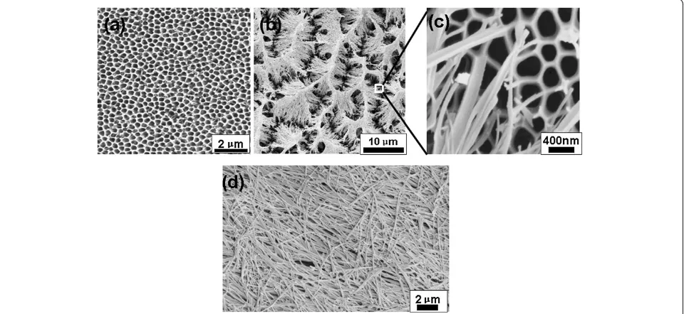
under a constant voltage of 9 V and a temperature of 90°C to 100°C for 10 min. During this process, the aluminum was used as the anode and a platinum plate as the cath-ode. To obtain ordered nanopore arrays, we used a two-step anodizing process. The foil was anodized first in 0.3 M oxalic acid at 33 V at 0°C to 5°C for 14 h. It was then immersed in a mixed solution of 5.0 wt.% phosphoric acid and 1.8 wt.% chromic acid (1:1 in volume) at 60°C for 3 h to remove the alumina layer. In the second step, the sample was again anodized for 2 h under the same condi-tions and then, the underlying aluminum was removed in a CuCl2/HCl (13.5 g CuCl2in 100 ml of 35% HCl) solution to expose the back-end AAO barrier. Finally, for pore wid-ening, the sample was immersed in a 5.0 wt.% phosphoric acid solution at 30°C for 1 h. The scanning electron micro-scope (SEM) image of the fabricated porous AAO (sign with P-AAO) is present in Figure 1a. According the meas-urement result from the commercial software, the pore diameter and the pore spacing are approximately 302 ± 47 nm and 381 ± 52 nm, respectively.
[image:2.595.59.539.494.715.2]To obtain the nanowire network AAOs, we required the manufacturer to add a film-eroding process after the pore-widening process. The P-AAOs were immersed again in mixed solution of 5.0 wt.% phosphoric acid and 1.8 wt.% chromic acid (1:1 in volume) at 60°C. The walls of the nanopores were damaged by the mixed acid solu-tion, the nanopore structure fell down, and leaf-like nanowire cluster structure formed. Figure 1b shows the sample with a film-eroding time of 5 min, signed as W-AAO1. Figure 1c is the partial enlargement of W-AAO1, which show that the nanowire formed from the broken wall of nanopores. With further eroding, the nanowires formed from walls of nanopores became longer and
thinner and could no longer prop each other. Therefore, the nanowire cluster fell down, and the nanowires lied on the surface as a uniform random layer. Figure 1d is the SEM image of the AAO with a film-eroding time of 10 min, called W-AAO2. The average diameter of nanowire on W-AAO1 and W-AAO2 was measured to be 68 ± 16 nm and 57 ± 15 nm, respectively. As shown in Figure 1b,d, dense junctions between the nanowires exist in W-AAO1 and W-AAO2. Previous studies have certif-icated that great amount of sub-10-nm gaps exist in these nanowire network structures [39-41].
After depositing 50 nm of Au onto the surface of P-AAO, W-AAO1, and W-AAO2, large-area high-performance SERS substrates were fabricated and were assigned as P-AAO-Au, W-AAO1-Au, and W-AAO2-Au, respectively.
Detail of SERS spectra measurement
The measurement of SERS is same with our previous work [42]. Benzene thiol was used as the probe molecule. To ensure that a complete self-assembled monolayer (SAM) of benzene thiol was formed on the substrate surface, all of the SERS substrates were immersed in a 1 × 10⁻³M solu-tion of benzene thiol in ethanol for approximately 18 h
[image:3.595.58.538.392.654.2]and were subsequently rinsed with ethanol and dried in nitrogen [8,42]. All the Raman spectra were measured with a confocal Raman spectroscopic system (model inVia, Renishaw Hong Kong Ltd., Kowloon Bay, Hong Kong, China). The spectrograph uses 1,200 g mm−1 gratings, a 785-nm laser and a scan type of SynchroScan. The incident laser power was set to be 0.147 mW for all SERS substrates. All the SERS spectra were collected using × 50, NA = 0.5, long working distance objective and the laser spot size is about 2μm. SERS spectra were recorded with an accumulation time of 10 s. After the SAM of benzene thiol was formed on the substrate surface, a single scan was performed. To get an accurate approximation of the enhancement factors, we measured the neat Raman spectrum of benzene thiol. For the measurement of the neat Raman spectrum of benzene thiol, the power of the 785-nm laser was 1.031 mW, the accumulation time was 10 s, the spot size was 20μm, and the depth of focus was 18μm.
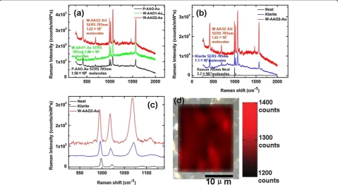
Figure 2a shows the Raman spectra of the benzene thiol SAM on the P-AAO-Au (black), W-AAO1-Au (green), and W-AAO2-Au (red) with all having been normalized to account for the accumulation time and laser power. To characterize the SERS performance of
Figure 2Comparison of substrates and neat benzene thiol,Raman spectra, and spatial mapping. (a)Comparison of the SERS of substrates P-AAO-Au, W-AAO1-Au, and W-AAO2-Au.(b)Comparison of the SERS of substrates W-AAO2-Au (red), Klarite® (blue), and neat Raman spectra (black) of benzene thiol collected at 785-nm incident.(c)Zoomed-in region of the spectra showing the three primary modes located near 1,000 cm−1, with the 998 cm−1used for calculation of the SERS enhancement factor. The number of molecules of benzene thiol that each
measurement is probing is denoted in the figure.(d)Spatial mapping of the SERS intensity at 998 cm−1of SERS substrate W-AAO2-Au over an
our substrates, commercial Klarite® substrates were used as reference samples which consists of gold-coated textured silicon (regular arrays of inverted pyramids of 1.5-μm wide and 0.7-μm deep) mounted on a glass micro-scope slide. Figure 2b shows the normalized Raman spec-tra of the benzene thiol SAM on the W-AAO2-Au (red), on the Klarite® substrate (blue), and neat thiophenol (black).
The calculation of EF
The average EFs were calculated from the following equation [8,42]:
EF¼ðISERS=IRamanÞ ðNRaman=NSERSÞ
whereISERSandIRamanare the normalized Raman inten-sity of SERS spectra and neat Raman spectrum of ben-zene thiol, respectively. NSERS and NRaman represent the numbers of molecules contributing to SERS signals and neat Raman signals of benzene thiol, respectively. ISERS and IRaman can be measured directly from the Raman spectra.NRamanis defined as follows [42]:
NRaman¼ρVMWNA
where ρ= 1.073 g mL−1 and MW= 110.18 g mol−1 are the density and molecular weight of benzene thiol, re-spectively, and V is the collection volume of the liquid sample monitor. NAis Avogadro's number.NSERS is de-fined as follows [42]:
NSERS¼ρsurfNASsurf
whereρsurfis the surface coverage of benzene thiol which has been reported as approximately 0.544 nmol cm−2 [8,42], and Ssurf is the surface area irradiated by exciting laser. For a clear comparison, NSERS and NRaman were quoted within Figure 2.
[image:4.595.304.538.629.707.2]As shown in Figure 2, the average EFs based on the neat benzene thiol are dependent on the choice of Raman mode strongly. However, the relative Raman enhancement between our SERS substrates (including Klarite® substrate) was found to be relatively independ-ent on the choice of Raman mode used for comparison. For comparison, the three Raman modes associated with vibrations about the aromatic ring are presented in Figure 2c. So, to get an accurate and comparable estima-tion of the average enhancement factor, Raman mode used for the calculation of the average EF must be se-lected carefully. Here, the intensities of the peak found at 998 cm−1, carbon-hydrogen wagging mode which is the furthest mode removed from the gold surface were used to compute the average EFs [8,42]. In addition, the average EF of Klarite® substrate was calculated to be 5.2 × 10⁶, which is reasonable because the enhancement
factor for the inverted pyramid structure of Klarite® sub-strates relative to a non-enhancing surface is rated to a lower bound of approximately 106[42].
Results and discussion
The average peak intensity at 998 cm−1, the number of molecules contributing to the Raman signal, the calcu-lated average EFs, and the relative standard deviation (RSD) for all SERS substrates are presented in Table 1. For each substrate, more than 80 spectra were collected at various positions to ensure that a reproducible SERS response was attained. Spatial mapping with an area larger than 20 μm × 20 μm of the SERS intensity of W-AAO2-Au was shown in Figure 2d as an example.
As shown in Figure 2a,b,c and Table 1, an obvious enhancement of Raman signal of the nanowire network AAO SERS substrates (W-AAO1-Au and W-AAO2-Au) is found, compared to that of porous AAO SERS sub-strate (P-AAO-Au). The Raman signal of W-AAO2-Au is the strongest in all of the SERS substrates (including the Klarite® substrate). Table 1 also shows a tremendous increase of average EF of the nanowire network AAO SERS substrate comparing with porous AAO SERS sub-strate. The average EFs of W-AAO1-Au and W-AAO2-Au are 2.56 × 10⁶and 5.93 × 10⁶, about 14 and 35 times larger than that of P-AAO-Au (1.56 × 10⁵), respectively. Moreover, the average EF of our best SERS substrate, W-AAO2-Au, is larger than that of commercial Klarite® substrate by about 14%. The enormous average EFs of the nanowire network AAOs SERS substrates suggest that a gigantic electromagnetic enhancement occurs in the dense ‘hot junctions’ between the nanowires which exist in W-AAO1-Au and W-AAO2-Au. Additionally, the higher density of hot junctions that exist in W-AAO2-Au is the reason the peak intensity and the average EF of W-AAO2-Au are larger than that of W-AAO1-Au.
The spatial mapping with an area larger than 20μm ×
20 μm of the SERS intensity of W-AAO2-Au as shown
in Figure 2d and the RSDs that are shown in Table 1 point out that the nanowire structure AAOs, especially W-AAO2-Au, are very uniform. Comparing with the RSD of P-AAO-Au, the RSD of W-AAO1-Au is larger, which is caused by the non-uniform leaf-like nanowire
Table 1 SERS performance parameters of SERS substrates
Sample Peak intensity (counts/mW/s)
Number of molecules
Average EF
RSD (%)
P-AAO-Au 351.62 1.58 × 10⁸ 1.65 × 10⁵ 8.02
W-AAO1-Au 997.92 2.88 × 10⁷ 2.56 × 10⁶ 8.25
W-AAO2-Au 1295.04 1.62 × 10⁷ 5.93 × 10⁶ 6.43
Klarite® 772.58 1.10 × 10⁷ 5.21 × 10⁶ 7.12
The average peak intensity at 998 cm−1
cluster structure on the surface of W-AAO1-Au, and the RSD of W-AAO2-Au is smallest, which can be at-tributed to the uniform random nanowire network structure formed on the surface of W-AAO2-Au. The reproducibility of our best SERS substrate, W-AAO2-Au, is even better than that of commercial Klarite® sub-strate. The RSDs of W-AAO2-Au in the SERS intensities were limited to only approximately 7% within a given substrate (that of Klarite® substrate is 7.12%), and the maximum deviation in the SERS intensities was limited to approximately 13%. The SERS response at a given point on the substrate was found to be highly reprodu-cible, with variations in the detected response being limited to about 5%.
Conclusions
In conclusion, we provide a simple, low-cost, and high output method, based on the riper production process of porous AAO, to fabricate large-area nanowire struc-ture AAO which can be used as high-performance SERS substrate. The measured Raman spectra and the calcu-lated average EFs show that compared with the porous AAO and commercial Klarite® substrates, the nanowire structure AAO SERS substrates are sensitive and uni-form in large area. The average EF of our sensitive SERS substrate can reach 5.93 × 10⁶, which indicates the exist-ence of enormous electromagnetic enhancement in the nanowire network AAO substrate. Repeated measure-ments and spatial mapping show an excellent uniformity of the nanowire network AAO substrate. The RSDs in the SERS intensities of W-AAO2-Au are limited to ap-proximately 7%. For these superiorities, we believe that our nanowire structure AAO SERS substrates are suit-able choice for chemical/biological sensing applications.
Abbreviations
AAO:Anodized aluminum oxide; EF: Raman enhancement factor; RSD: Relative standard deviation; SAM: Self-assembled monolayer; SEM: Scanning electron microscope; SERS: Surface-enhanced Raman scattering; SPR: Surface plasmon resonance.
Competing interests
The authors declare that they have no competing interests.
Authors' contributions
QJ conceived of the study, carried out the fabrication of the SERS substrates, the measurement and analysis, the simulation, and drafted the manuscript. LY (Yudong) participated in the SERS spectra analysis and discussion. YM, PJ, LY (Yue), and WQ participated in the SEM measurements and SERS spectra measurements. CZ, WW, and YX participated in the fabrication of the SERS substrates. XJ and SQ were the PI of the project and participated in the design and coordination of the study and revised the manuscript. All authors read and approved the final manuscript.
Authors' information
QJ is a lecturer at Nankai University. His research interest includes fabrication of the nanostructure, nonlinear optical properties of nanostructures, fanoresonance, and surface plasmon resonance and their applications in SERS, sensor, and so on.
Acknowledgements
This study is supported by the National Natural Science Foundation of China under grant no. 61178004, the Tianjin Natural Science Foundation under grant nos. 12JCQNJC01100 and 06TXTJJC13500, the Doctoral Program of Higher Education of China under grant no. 20110031120005, the Program for Changjiang Scholars and Innovative Research Team in Nankai University, 111 Project under grant no. B07013, and Fundamental Research Funds for the Central Universities. We are also very grateful to Professor Zhou Q. L., Professor Xie J. H., and their group for providing solution of benzene thiol in ethanol.
Received: 25 October 2013 Accepted: 15 November 2013 Published: 21 November 2013
References
1. Nie S, Remory S:Probing single molecules and single nanoparticles by surface-enhanced Raman scattering.Science1997,275:1102–1106. 2. Kneipp K, Wang Y, Kneipp H, Perelman LT, Itzkan I, Dasari RR, Field MS:Field
single molecule detection using surface-enhanced Raman scattering. Phys Rev Lett1997,78:1667–1670.
3. Li JF, Huang YF, Ding Y, Yang ZL, Li SB, Zhou XS, Fan FR, Zhang W, Zhou ZY, Wu DY, Ren B, Wang ZL, Tian ZQ:Shell-isolated nanoparticle-enhanced Raman spectroscopy.Nature2010,464:392–395. 4. Liang HY, Li ZP, Wang WZ, Wu YS, Xu HX:Highly surface-roughened
"flower-like" silver nanoparticles for extremely sensitive substrates of surface-enhanced Raman scattering.Adv Mater2009,21:4614–4618. 5. Liu FX, Cao ZS, Tang CJ, Chen L, Wang ZL:Ultrathin diamond-like carbon
film coated silver nanoparticles-based substrates for surface-enhanced Raman spectroscopy.ACS Nano2010,4:2643–2648.
6. Ryckman JD, Liscidini M, Sipe JE, Weiss SM:Direct imprinting of porous substrates: a rapid and low-cost approach for patterning porous nanomaterials.Nano Lett2011,11:1857–1862.
7. Schmidt MS, Hubner J, Boisen A:Large area fabrication of leaning silicon nanopillars for surface enhanced Raman spectroscopy.Adv Mater2012,
24:11–18.
8. Caldwell JD, Glembocki O, Bezares FJ, Bassim ND, Rendell RW, Feygelson M, Ukaegbu M, Kasica R, Shirey L, Hosten C:Plasmonic nanopillar arrays for large-area, high-enhancement surface-enhanced Raman scattering sensors. ACS Nano2011,5:4046–4055.
9. Zhang L, Lang X, Hirata A, Chen M:Wrinkled nanoporous gold films with ultrahigh surface-enhanced Raman scattering enhancement.ACS Nano
2011,5:4407–4413.
10. Duan H, Hu H, Kumar K, Shen Z, Yang JKW:Direct and reliable patterning of plasmonic nanostructures with sub-10-nm gaps.ACS Nano2011,
5:7593–7600.
11. Wang HH, Liu CY, Wu SB, Liu NW, Peng CY, Chan TH, Hsu CF, Wang JK, Wang YL:Highly Raman-enhancing substrates based on silver nanoparticle arrays with tunable sub-10 nm gaps.Adv Mater2006,18:491.
12. Siegfried T, Ekinci Y, Solak HH, Martin OJF, Sigg H:Fabrication of sub-10 nm gap arrays over large areas for plasmonic sensors.Appl Phys Lett2011,
99:263302.
13. Cho WJ, Kim Y, Kim JK:Ultrahigh-density array of silver nanoclusters for SERS substrate with high sensitivity and excellent reproducibility. ACS Nano2012,6:249–255.
14. Hu X, Meng G, Huang Q, Xu W, Han F, Sun K, Xu Q, Wang Z:Large-scale homogeneously distributed Ag-NPs with sub-10 nm gaps assembled on a two-layered honeycomb-like TiO2 film as sensitive and reproducible SERS substrates.Nanotechnology2012,23:385705.
15. Jin M, van Wolferen H, Wormeester H, van den Berg A, Carlen ET:Large-area nanogap plasmon resonator arrays for plasmonics applications.Nanoscale
2012,4:4712–4718.
16. Alexander KD, Skinner K, Zhang S, Wei H, Lopez R:Tunable SERS in gold nanorod dimers through strain control on an elastomeric substrate. Nano Lett2010,10:4488–4493.
17. Zhang X-Y, Hu A, Zhang T, Lei W, Xue X-J, Zhou Y, Duley WW:Self-assembly of large-scale and ultrathin silver nanoplate films with tunable plasmon resonance properties.ACS Nano2011,5:9082–9092.
19. Kostovski G, Chinnasamy U, Jayawardhana S, Stoddart PR, Mitchell A:
Sub-15 nm optical fiber nanoimprint lithography: a parallel, self-aligned and portable approach.Ad Materials2011,23:531.
20. Gong J, Lipomi DJ, Deng J, Nie Z, Chen X, Randall NX, Nair R, Whitesides GM:Micro- and nanopatterning of inorganic and polymeric substrates by indentation lithography.Nano Lett2010,10:2702–2708.
21. Liu GL, Lee LP:Nanowell surface enhanced Raman scattering arrays fabricated by soft-lithography for label-free biomolecular detections in integrated microfluidics.Appl Phys Lett2005,87:074101.
22. Xu M, Lu N, Xu H, Qi D, Wang Y, Chi L:Fabrication of functional silver nanobowl arrays via sphere lithography.Langmuir2009,25:11216–11220. 23. Xue M, Zhang Z, Zhu N, Wang F, Zhao XS, Cao T:Transfer printing of
metal nanoparticles with controllable dimensions, placement, and reproducible surface-enhanced Raman scattering effects.Langmuir2009,
25:4347–4351.
24. Wu W, Hu M, Ou FS, Li Z, Williams RS:Cones fabricated by 3D nanoimprint lithography for highly sensitive surface enhanced Raman spectroscopy.Nanotechnology2010,21:255502.
25. Im H, Bantz KC, Lindquist NC, Haynes CL, Oh S-H:Vertically oriented sub-10-nm plasmonic nanogap arrays.Nano Lett2010,10:2231–2236. 26. Diebold ED, Mack NH, Doom SK, Mazur E:Femtosecond laser-nanostructured
substrates for surface-enhanced Raman scattering.Langmuir2009,
25:1790–1794.
27. Lin C-H, Jiang L, Chai Y-H, Xiao H, Chen S-J, Tsai H-L:One-step fabrication of nanostructures by femtosecond laser for surface-enhanced Raman scattering.Opt Express2009,17:21581–21589.
28. Jiang L, Ying D, Li X, Lu Y:Two-step femtosecond laser pulse train fabrication of nanostructured substrates for highly surface-enhanced Raman scattering.Opt Lett2012,37:3648–3650.
29. Wang C, Chang Y-C, Yao J, Luo C, Yin S, Ruffin P, Brantley C, Edwards E:
Surface enhanced Raman spectroscopy by interfered femtosecond laser created nanostructures.Appl Phys Lett2012,100:023107.
30. Terekhov SN, Mojzes P, Kachan SM, Mukhurov NI, Zhvavyi SP, Panarin AY, Khodasevich IA, Orlovich VA, Thorel A, Grillon F, Turpin PY:A comparative study of surface-enhanced Raman scattering from silver-coated anodic aluminum oxide and porous silicon.J Raman Spectrosc2011,42:12–20. 31. Chung AJ, Huh YS, Erickson D:Large area flexible SERS active substrates
using engineered nanostructures.Nanoscale2011,3:2903–2908. 32. Dickey MD, Weiss EA, Smythe EJ, Chiechi RC, Capasso F, Whitesides GM:
Fabrication of arrays of metal and metal oxide nanotubes by shadow evaporation.ACS Nano2008,2:800–808.
33. Giallongo G, Durante C, Pilot R, Garoli D, Bozio R, Romanato F, Gennaro A, Rizzi GA, Granozzi G:Growth and optical properties of silver
nanostructures obtained on connected anodic aluminum oxide templates.Nanotechnology2012,23:325604.
34. Huang C-H, Lin H-Y, Chen S, Liu C-Y, Chui H-C, Tzeng Y:Electrochemically fabricated self-aligned 2-D silver/alumina arrays as reliable SERS sensors. Opt Express2011,19:11441–11450.
35. Huang Z, Meng G, Huang Q, Chen B, Zhu C, Zhang Z:Large-area Ag nanorod array substrates for SERS: AAO template-assisted fabrication, functionalization, and application in detection PCBs.J Raman Spectrosc
2013,44:240–246.
36. Ruan C, Eres G, Wang W, Zhang Z, Gu B:Controlled fabrication of nanopillar arrays as active substrates for surface-enhanced Raman spectroscopy.Langmuir2007,23:5757–5760.
37. Prokes SM, Alexson DA, Glembocki OJ, Park HD, Rendell RW:Effect of crossing geometry on the plasmonic behavior of dielectric core/metal sheath nanowires.Appl Phys Lett2009,94:093105.
38. Prokes SM, Glembocki OJ, Rendell RW, Ancona MG:Enhanced plasmon coupling in crossed dielectric/metal nanowire composite geometries and applications to surface-enhanced Raman spectroscopy.Appl Phys Lett2007,90:093105.
39. Tao A, Kim F, Hess C, Goldberger J, He RR, Sun YG, Xia YN, Yang PD:
Langmuir-Blodgett silver nanowire monolayers for molecular sensing using surface-enhanced Raman spectroscopy.Nano Lett2003,
3:1229–1233.
40. Tian C, Ding C, Liu S, Yang S, Song X, Ding B, Li Z, Fang J:Nanoparticle attachment on silver corrugated-wire nanoantenna for large increases of surface-enhanced Raman scattering.ACS Nano2011,5:9442–9449. 41. Feng M, Zhang M, Song J-M, Li X-G, Yu S-H:Ultralong silver trimolybdate
nanowires: synthesis, phase transformation, stability, and their
photocatalytic, optical, and electrical properties.ACS Nano2011,
5:6726–6735.
42. Qi J, Li Y, Yang M, Wu Q, Chen Z, Wang W, Lu W, Yu X, Xu J, Sun Q:
Large-area high-performance SERS substrates with deep controllable sub-10-nm gap structure fabricated by depositing Au film on the cicada wing.Nanoscale Res Lett2013,8:437.
doi:10.1186/1556-276X-8-495
Cite this article as:Jiweiet al.:Fabrication of nanowire network AAO
and its application in SERS.Nanoscale Research Letters20138:495.
Submit your manuscript to a
journal and benefi t from:
7Convenient online submission
7Rigorous peer review
7Immediate publication on acceptance
7Open access: articles freely available online
7High visibility within the fi eld
7Retaining the copyright to your article