N A N O E X P R E S S
Open Access
Preparation and Characterization of
Solution-Processed Nanocrystalline
p
-Type
CuAlO
2
Thin-Film Transistors
Shuang Li, Xinan Zhang
*, Penglin Zhang, Xianwen Sun, Haiwu Zheng and Weifeng Zhang
Abstract
The development ofp-type metal oxide thin-film transistors (TFTs) is far behind then-type counterparts. Here,p-type CuAlO2thin films were deposited by spin coating and annealed in nitrogen atmosphere at different temperature. The effect of post-annealing temperature on the microstructure, chemical compositions, morphology, and optical
properties of the thin films was investigated systematically. The phase conversion from a mixture of CuAl2O4and CuO to nanocrystalline CuAlO2was achieved when annealing temperature was higher than 900 °C, as well as the
transmittance, optical energy band gap, grain size, and surface roughness of the films increase with the increase of annealing temperature. Next, bottom-gatep-type TFTs with CuAlO2channel layer were fabricated on SiO2/Si substrate. It was found that the TFT performance was strongly dependent on the physical properties and the chemical
composition of channel layer. The optimized nanocrystalline CuAlO2TFT exhibits a threshold voltage of−1.3 V, a mobility of ~ 0.1 cm2V−1s−1, and a current on/off ratio of ~ 103. This report on solution-processedp-type CuAlO2TFTs represents a significant progress towards low-cost complementary metal oxide semiconductor logic circuits.
Keywords:Solution-processed,p-type thin-film transistor, Nanocrystalline films, Mobility
Background
Over the past decades, metal oxide thin-film transistors (TFTs) have been extensively investigated for the next-generation active-matrix liquid crystal displays, or-ganic light-emitting diode displays, and other emerging electronic circuits applications due to their excellent electrical properties and outstanding optical transpar-ency [1,2]. However, a majority of the metal oxide TFTs reported to date were focused on n-type materials [3]. The p-type oxide semiconductors are usually character-ized with localcharacter-ized oxygen2porbitals with large electro-negativity, self-compensation from oxygen vacancies, and the incorporation of hydrogen as an unintentional donor. Therefore, it is difficult in achieving effective hole doping [4]. Up to now, only a fewp-type oxide materials (Cu2O, CuO, SnO, etc.) were proved to be suitable for
TFT application [5,6], but their performance lags far be-hind ofn-type counterparts. This limits the development
of all oxide p-n junctions and complementary metal oxide semiconductor (CMOS) logic circuits.
To obtain a good p-type metal oxide, it is critical to modify the energy band structure and reduce the Cou-lomb force exerted by the oxygen ions on holes. thus motivating the discovery of a group ofp-type delafossite oxides, such as CuMO2(M=Al, Ga, In) and SrCu2O2[7,
8]. Among them, CuAlO2 has a wide bandgap of ~
3.5 eV, and its valence band maximums are dominated by a large hybridization of the oxygen orbitals with 3d10 electrons in the Cu1+closed shell, which leads to a dis-persive valence band. Meanwhile, the cations with closed shells (d10s0) are beneficial to achieve high optical trans-parency because such an electronic structure can avoid light absorption from the so-called d-d transitions. Therefore, it has attracted considerable attention since the first fabrication in 1997 [9]. However, there are only a few reports focusing onp-type TFTs using CuAlO2as
channel layers. The primary difficulty is poor crystallinity and impurity phases, such as Cu2O, CuO, Al2O3, and
CuAl2O4. The first report of a CuAlO2 TFT was
fabri-cated by magnetron sputtering, and the device exhibits a * Correspondence:[email protected]
School of Physics and Electronics, Key Laboratory of Photovoltaic Materials, Henan University, Kaifeng 475004, People’s Republic of China
the thin films was investigated systematically. Finally, bottom-gate TFTs using the obtained nanocrystalline CuAlO2thin films as channel layers were fabricated and
they exhibit a mobility of ~ 0.1 cm2V−1s−1, a threshold voltage of−1.3 V, and a current on/off ratio of ~ 10 [3].
Methods/Experimental
Precursor Preparation and Thin-Film Fabrication
The CuAlO2 thin films were prepared by spin coating
using copper nitrate trihydrate (Cu(NO3)2·3H2O) and
aluminum nitrate nonahydrate (Al(NO3)3·9H2O) as
starting materials. The molar ratio of two metal salts is 1:1, and the concentration of each salt in ethylene glycol methylether is 0.2 mol/L; acetylacetone was added to form a stable solution in deep green. The entire mixing process was carried out in 80 °C water bath with stirring. Prior to film deposition, the substrates were ultrasonic-ally cleaned with acetone, ethanol, and deionized water for 5 min in each solution. Then, the final precursor was spin-coated with a low rotating speed of 500 rpm for 9 s and followed by a high rotating speed of 5000 rpm for 30 s. After spin-coating, the substrate was annealed at 350 °C for 20 min. The procedures from coating to an-nealing were repeated four times until the desired thick-ness (~ 40 nm) of the films was reached. Finally, the as-deposited films were annealed at 700–1000 °C for 2 h in nitrogen atmosphere and cooled down to room temperature at same atmosphere.
Fabrication of CuAlO2TFTs
The CuAlO2 TFTs with a bottom-gate structure were
fabricated on SiO2/Si substrate. Three
hundred-nanometer-thick SiO2serves as the gate dielectric. After
CuAlO2film deposition, 50 nm gold source/drain
elec-trodes were thermal evaporated on the channel layer through a shadow mask. The evaporation rate was 0.08 nm/s, and the channel width (W) and length (L) were 1000 μm and 100 μm, respectively. Finally, an in-dium layer was welded to the Si substrate as the back-gate electrode.
Film and TFT Characterization
The CuAlO2film structure was studied by X-ray
diffrac-tion (XRD, DX2500) with CuKα radiation (λ=
tometer (Varian Cary 5000). The electrical characteristics were measured by a semiconductor par-ameter analyzer (Keithley 2612B).
Results and Discussion
Figure 1a shows the XRD patterns of CuAlO2 thin films
annealed at a different temperature. For the film annealed at 700 °C, only weak CuO phase diffraction peaks at 35.8° and 38.9° were observed, indicating that 700 °C is not enough for the formation of CuAlO2phase [11]. Two new
peaks at 31.7° and 37.1° assigned to CuAlO2and CuAl2O4
phases, respectively, were observed after 800 °C annealing. When the temperature reached to 900 °C, the intensity of the CuO peaks decrease and the CuAl2O4phase peaks
dis-appear. Several new peaks at 36.8°, 42.5°, 48.5°, 57.5°, and 31.7°, assigned to CuAlO2 phase, dominated the film [9,
12]. The temperature was further increased to 1000 °C, the peaks intensity increased, and single CuAlO2 phase were
obtained. The enhancement of the crystallinity may be at-tributed to the fact that more energy absorption accelerated the growth of crystallites at higher annealing temperature.
Figure 1b shows the Raman spectra of CuAlO2 thin
films. The four-atom primitive cell of delafossite struc-ture CuAlO2leads to 12 normal modes, but only the A1g
(416 cm−1) and Eg (771 cm−1) modes are Raman active.
As shown in Fig.1b, it is obvious that two Raman vibra-tion modes, A1g and Eg, both are present for all films
[13]. Unlike bulk analysis of XRD, Raman scattering originates from the molecular vibration and lattice vibra-tion that can detect Raman active molecule vibrate from a very small amount of concentration. That explains the existence of CuAlO2phase in the 700 °C annealed film,
which is not observable in XRD spectrum. Others peaks at 798 cm−1, 297 cm−1, and 632 cm−1were also observed which are assigned to the F2gmode of CuAl2O4, Ag, and
Bg modes of CuO, respectively [14]. The peaks of CuO
and CuAl2O4 phases decrease as the annealing
temperature increases from 700 to 1000 °C, and both phases convert to phase CuAlO2 after 1000 °C
anneal-ing, which is consistent with XRD results.
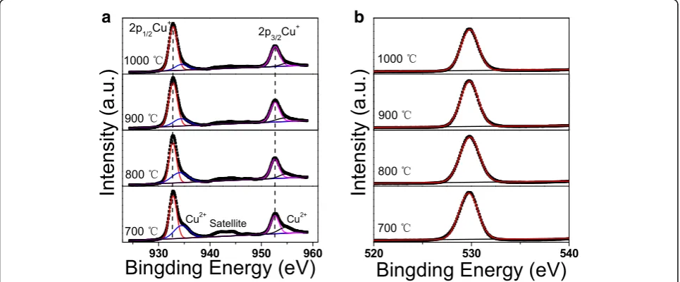
To understand the chemical compositions of CuAlO2
be fitted into two peaks located at ~ 932.8 and ~ 934.2 eV, which can be attributed to Cu+ and Cu2+, re-spectively. Similarly, fitted Cu 2p1/2 deconvolution two peaks are centered at ~ 952.6 (Cu+) and ~ 954.1 eV (Cu2
+
), respectively [15]. Since the spin-orbital splitting of Cu 2p is ~ 19.8 eV, the 2p3/2 and 2p1/2 peaks were not constrained for the area ratio during fitting. Neverthe-less, the area ratio of the Cu 2p3/2 peak and the Cu 2p1/2 peak is ~ 1.90, being close to the ideal value of 2 determined from electron state densities [14]. The domi-nated peaks at ~ 932.8 eV (Cu+) and ~ 952.6 eV (Cu+) indicate that Cu cations mainly exist in Cu+ form in CuAlO2lattice. Note that Cu2+state is presented in all
films, even no CuO peaks were detected in the high temperature annealed samples by XRD. Meanwhile, the satellite peaks observed from 941.2 to 944.4 eV also im-plied the presence of CuO. However, satellite peaks are almost negligible after high-temperature annealing,
which is consistent with the above XRD observations. Quantitative analysis of the XPS spectra gave Cu+/ [Cu++Cu2+] atomic ratios of 62.5%, 68.9%, 73.7%, and 78.9% for CuAlO2thin films annealed at 700, 800, 900,
and 1000 °C, respectively, indicating reduction of Cu2+ with the increase of annealing temperature [10,16]. The XPS O 1s peaks are shown in Fig.2b. It was interesting that the binding energies exhibit symmetrical dominant peaks centered at ~ 529.8 eV, indicating most of oxygen atom are bonded to nearest neighbor metal ions (Cu+, Al3+, or Cu2+) in the lattice. It should be noted that the peak at ~ 531.3 eV, attributed to oxygen-related defects, can hardly be distinguished. This result can be explained by the introduction of surface etch process and high crystallization quality.
The surface morphologies of the CuAlO2 thin films
were observed by SEM, as shown in Fig.3a. All the films exhibit continuous, smooth, and dense structure
a
b
Fig. 1aXRD patterns.bRaman spectra of the CuAlO2thin films annealed at different temperature
a
b
[image:3.595.57.540.87.250.2] [image:3.595.57.540.514.714.2]morphology without obvious micro-cracks. The grain size is homogeneous and increases with the increase of annealing temperature. The gradually enlarged grain size would lead to the fewer grain boundaries, which act as trapping sites and significantly reduce the mobility for the nanocrystalline CuAlO2 films [17]. Thus, the
CuAlO2 thin films annealing at high temperature is
beneficial to the charge transport and may result high performance TFTs [18]. Surface roughness is another factor which can seriously influence the electrical per-formance of oxide TFTs [19]. To obtain the root mean square (RMS) roughness, the CuAlO2thin films were
in-vestigated by AFM, as shown in Fig. 3b. The RMS roughness of films annealed at 700 °C, 800 °C, 900 °C, and 1000 °C were 0.92, 1.82, 2.12, and 2.96 nm, respect-ively. Obviously, the RMS increases with the increase of annealing temperature. Generally, rough surface would result in presence of electrical defects or trapping sites resulting in inferior device performance [20]. Therefore, it was supposed that there should be a competition rela-tion between grain size and surface roughness to affect the performance of nanocrystalline oxide TFTs.
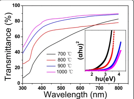
The optical transmission spectra of the CuAlO2 thin
films on fused silica were measured in wavelength range from 200 to 800 nm, as shown in Fig. 4. It was observed that all films have steep absorption edge and strong ultraviolet absorption, which is an indica-tion of the good crystallinity of the films. The average transmittance in the visible light region was calculated from ~ 60 to ~ 80%, increasing with the increase of annealing temperature. Tauc’s relation αhν=A(hν− Eg)
1/2
is carried out to calculate the optical band gap, where α is the absorption coefficient, A is the con-stant for a direct transition, h is the Planck’s constant, and ν is the photon frequency [21]. The value of Eg
is given by the linear extrapolation of the plot of
(αhν)2 versus hν to the energy axis, as shown in the inset of Fig. 4. The Eg were calculated to be 3.25 eV, 3.40 eV, 3.60 eV, and 3.80 eV for the CuAlO2 thin
films annealed at 700 °C, 800 °C, 900 °C, and 1000 ° C, respectively.
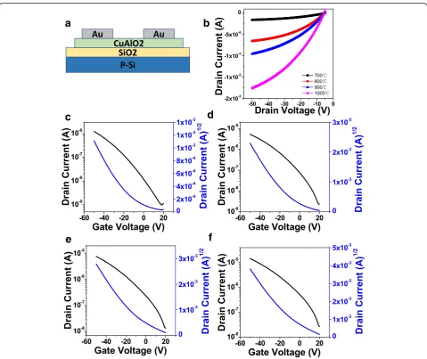
Finally, we fabricated the bottom-gate top-contact TFTs on SiO2/p-Si substrates to investigate the electrical
performance of CuAlO2 as channel layers. The
sche-matic diagram of device is illustrated in Fig.5a. The out-put curves of the CuAlO2TFTs at a gate-source voltage
(VGS) of −50 V are shown in Fig.5b. It clearly indicates
the on-state current (Ion) increases with the increase of
annealing temperature. This is mainly attributed to the elimination of insulator-like CuAl2O4phase and the
en-hancement of nanocrystalline CuAlO2phase. The
trans-fer curves are shown in Fig.5c–f, and the CuAlO2TFTs
exhibit a typical p-type behavior. All the devices show a moderate on/off current ratio (Ion/Ioff) of ~ 103 which
perhaps can be further improved by optimizing channel thickness, cation doping, or changing source/drain ma-terial [22–24]. The threshold voltage (VT) is determined
as a horizontal axis intercept of a linear fitting to the
IDS1/2-VGS curve. TheVTshift towards the positive with
Fig. 3aSEM.bAFM of the CuAlO2thin films annealed at different temperature
Fig. 4The optical transmission spectra for CuAlO2films annealed at
different temperature. The inset shows a plot of (αhν)2vs. hνof
[image:4.595.57.539.88.238.2] [image:4.595.306.539.521.693.2]the increase of annealing temperature. The filed effect mobility (μFE), the subthreshold slope (SS), and the interface trap density (Nt) can be calculated by the
fol-lowing equations [25,26]:
IDS¼ 1 2μFECOX
W
L ðVGS−VTÞ
2 ð
1Þ
SS¼ d log10IDS
dVGS
−1
ð2Þ
Nt¼
SSlogð Þe kT=q −1
Cox
q
ð3Þ
where k is the Boltzmann constant, T is the temperature,q is the elementary charge of electron, and
Cox is the areal capacitance of the gate insulator [27].
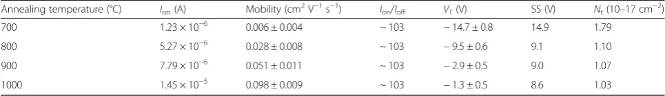
The key electrical parameters of the devices are listed in Table1. It can be seen the SS values, largely higher than reported n-type devices, decrease with the increase of annealing temperature, which is consistent with the trend of VT. The results can be explained by the reduction of
traps at the channel/dielectric interface [28]. The μFE values increase from 0.006 to 0.098 cm2V−1s−1as the an-nealing temperature increased from 700 to 1000 °C, which indicates an improvement of hole transport due to phase conversion from a mixture to nanocrystalline CuAlO2and
enlargement of grain size. The μFE are lower than solution-processed CuCrO2 TFTs reported by Nie et al
[16]. The reason may be the delafossite nanocrystalline CuAlO2structure is lack of Cu-O-Cu lattice content than
that of CuCrO2[29]. In spite of the annealing temperature
of the devices is high for practical applications, this is the first report about solution-processed CuAlO2 TFTs.
a
c
e
f
d
b
Fig. 5aSchematic diagram of the CuAlO2TFTs.bSummarized output curves.c–fTransfer curves of the CuAlO2TFTs annealed at 700 °C, 800 °C,
[image:5.595.58.538.85.488.2] [image:5.595.73.207.586.681.2]sis is now underway [23,30,31].
Conclusions
In summary, solution-processed CuAlO2thin films were
fabricated and annealed in nitrogen atmosphere at dif-ferent temperature. With the temperature increased from 700 to 1000 °C, the film structure phase transforms from a mixture of CuAl2O4and CuO to nanocrystalline
CuAlO2, as well as the optical transmittance, energy
band gap, grain size, and surface roughness of the films increase. The p-type CuAlO2 TFTs performance was
strongly dependent on the physical properties and the chemical composition of channel layer. The optimized nanocrystalline CuAlO2TFT exhibits a threshold voltage
of−1.3 V, a mobility of ~ 0.1 cm2V−1s−1, and a current on/off ratio of ~ 103. Compared to vacuum-based mag-netron sputtering, our work demonstrates a low-cost, solution-processed CuAlO2 TFTs, which represents an
important advancement towards the development of complementary metal oxide semiconductor logic circuits.
Abbreviations
AFM:Atomic force microscopy;Cox: The areal capacitance of the gate
insulator;Ion/Ioff: On/off current ratio;k: The Boltzmann constant;L: The
channel length;Nt: The interface trap density;q: The elementary charge of
electron; SEM: Scanning electron microscopy; SS: The subthreshold slope;
T: The absolute temperature; TFTs: Thin-film transistors;VT: Threshold voltage;
W: The channel width; XPS: X-ray photoelectron spectroscopy; XRD: X-ray diffraction;μFE: Filed effect mobility
Funding
This work was supported by the National Natural Science Foundation of China (U1504625), Youth Backbone Teacher Training Program in Henan province (2017GGJS021), Program for Innovative Research Team in Science and Technology in University of Henan Province (19IRTSTHN019), and Foundation of Henan Educational Committee (12A510003).
Availability of Data and Materials Presented in the main paper.
Authors’Contributions
SL carried out the main part of the experiments and drafted the manuscript. XZ designed the experiment and polished the manuscript. PZ participated in the measurements and performed the analysis. XS and HZ participated in the design of the study. WZ gave suggestions on the experimental design and polished the manuscript. All authors read and approved the final manuscript.
Competing Interests
The authors declare that they have no competing interests.
published maps and institutional affiliations.
Received: 28 May 2018 Accepted: 21 August 2018
References
1. Li Z-Y, Yang H-Z, Chen S-C, Lu Y-B, Xin Y-Q, Yang T-L, Sun H (2018) Impact of active layer thickness of nitrogen-doped In–Sn–Zn–O films on materials and thin film transistor performances. J Phys D Appl Phys 51(17):175101 2. Yu X, Marks TJ, Facchetti A (2016) Metal oxides for optoelectronic
applications. Nat Mater 15(4):383–396
3. Park JS, Maeng W-J, Kim H-S, Park J-S (2012) Review of recent developments in amorphous oxide semiconductor thin-film transistor devices. Thin Solid Films 520(6):1679–1693
4. Wang Z, Nayak PK, Caraveo-Frescas JA, Alshareef HN (2016) Recent developments in p-type oxide semiconductor materials and devices. Adv Mater 28(20):3831–3892
5. Sung S-Y, Kim S-Y, Jo K-M, Lee J-H, Kim J-J, Kim S-G, Chai K-H, Pearton SJ, Norton DP, Heo Y-W (2010) Fabrication of p-channel thin-film transistors using CuO active layers deposited at low temperature. Appl Phys Lett 97(22):222109
6. Yabuta H, Kaji N, Hayashi R, Kumomi H, Nomura K, Kamiya T, Hirano M, Hosono H (2010) Sputtering formation of p-type SnO thin-film transistors on glass toward oxide complimentary circuits. Appl Phys Lett 97(7):072111 7. Yanagi H, Hase T, Ibuki S, Ueda K, Hosono H (2001) Bipolarity in electrical
conduction of transparent oxide semiconductor CuInO2 with delafossite structure. Appl Phys Lett 78(11):1583–1585
8. Nagarajan R, Draeseke AD, Sleight AW, Tate J (2001) p-type conductivity in CuCr1−xMgxO2 films and powders. J Appl Phys 89(12):8022–8025 9. Kawazoe H, Yasukawa M, Hyodo H, Kurita M, Yanagi H, Hosono H (1997) P-type
electrical conduction in transparent thin films of CuAlO2. nature 389:939–942 10. Yao ZQ, He B, Zhang L, Zhuang CQ, Ng TW, Liu SL, Vogel M, Kumar A,
Zhang WJ, Lee CS, Lee ST, Jiang X (2012) Energy band engineering and controlled p-type conductivity of CuAlO2 thin films by nonisovalent Cu-O alloying. Appl Phys Lett 100(6):062102
11. Jiang HF, Lei HC, Zhu XB, Li G, Yang ZR, Song WH, Dai JM, Sun YP, Fu YK (2009) Effects of citric acid on properties of single phase CuAlO2 thin films derived by chemical solution deposition. J Alloys Compd 487(1–2):404–408 12. Ehara T, Abe H, Iizaka R, Abe K, Sato T (2017) Crystalline orientation control in sol–gel preparation of CuAlO2 thin films. J Sol-Gel Sci Technol 82(2):363–369 13. Byrne D, Cowley A, Bennett N, McGlynn E (2014) The luminescent
properties of CuAlO2. J Mater Chem C 2(37):7859–7868
14. Liu S, Wu Z, Zhang Y, Yao Z, Fan J, Zhang Y, Hu J, Zhang P, Shao G (2015) Strong temperature-dependent crystallization, phase transition, optical and electrical characteristics of p-type CuAlO2 thin films. Phys Chem Chem Phys 17(1):557–562
15. Ghosh CK, Popuri SR, Mahesh TU, Chattopadhyay KK (2009) Preparation of nanocrystalline CuAlO2 through sol–gel route. J Sol-Gel Sci Technol 52(1):75–81 16. Nie S, Liu A, Meng Y, Shin B, Liu G, Shan F (2018) Solution-processed ternary
p-type CuCrO2 semiconductor thin films and their application in transistors. J Mater Chem C 6(6):1393–1398
17. Murali KR, Balasubramanian M (2013) Properties of CuAlO2 thin films deposited by polyacrylamide gel route. Mater Sci Semicond Process 16(1):38–42
[image:6.595.56.539.99.169.2]19. Hou JJ, Wang F, Han N, Zhu H, Fok K, Lam W, Yip S, Hung T, Lee JEY, Ho JC (2013) Diameter dependence of electron mobility in InGaAs nanowires. Appl Phys Lett 102(9):093112
20. Wang F, Yip S, Han N, Fok K, Lin H, Hou JJ, Dong G, Hung T, Chan KS, Ho JC (2013) Surface roughness induced electron mobility degradation in InAs nanowires. Nanotechnology 24(37):375202
21. Zhang X, Zhai J, Yu X, Ding L, Zhang W (2013) Fabrication and characterization of flexible Ag/ZnO Schottky diodes on polyimide substrates. Thin Solid Films 548:623–626
22. Qu Y, Yang J, Li Y, Zhang J, Wang Q, Song A, Xin Q (2018) Organic and inorganic passivation of p-type SnO thin-film transistors with different active layer thicknesses. Semicond Sci Technol 33(7):075001
23. Liu A, Zhu H, Guo Z, Meng Y, Liu G, Fortunato E, Martins R, Shan F (2017) Solution combustion synthesis: low-temperature processing for p-type Cu: NiO thin films for transparent electronics. Adv Mater 29:1701599 24. Zhang X, Wang B, Sun X, Zheng H, Li S, Zhang P, Zhang W (2018) Highly
transparent and conductive W-doped ZnO/Cu/W-doped ZnO multilayer source/drain electrodes for metal-oxide thin-film transistors. IEEE Electron Device Lett 39(7):967–970
25. Jiao Y, Zhang X, Zhai J, Yu X, Ding L, Zhang W (2013) Bottom-gate amorphous In2O3 thin film transistors fabricated by magnetron sputtering. Electron Mater Lett 9(3):279–282
26. Dahiya AS, Opoku C, Poulin-Vittrant G, Camara N, Daumont C,
Barbagiovanni EG, Franzo G, Mirabella S, Alquier D (2017) Flexible organic/ inorganic hybrid field-effect transistors with high performance and operational stability. ACS Appl Mater Interfaces 9(1):573–584 27. Liu A, Liu G, Zhu H, Shin B, Fortunato E, Martins R, Shan F (2016) Hole
mobility modulation of solution-processed nickel oxide thin-film transistor based on high-k dielectric. Appl Phys Lett 108(23):233506
28. Ding X, Qin C, Song J, Zhang J, Jiang X, Zhang Z (2017) The influence of hafnium doping on density of states in zinc oxide thin-film transistors deposited via atomic layer deposition. Nanoscale Res Lett 12(1):63 29. Sanal KC, Jayaraj MK (2014) Room temperature deposited p-channel
amorphous Cu 1−x Cr x O 2−δthin film transistors. Appl Surf Sci 315:274– 278
30. Zhang H, Meng Y, Song L, Luo L, Qin Y, Han N, Yang Z, Liu L, Ho JC, Wang F (2018) High-performance enhancement-mode thin-film transistors based on Mg-doped In2O3 nanofiber networks. Nano Res 11(3):1227–1237 31. Wang F, Song L, Zhang H, Meng Y, Luo L, Xi Y, Liu L, Han N, Yang Z, Tang J,