tDlEX
'"
STD-SASI1
(J[]
1"FEATURES
o STD-Z80 Bus Compatible o 4 MHz Operation
o Supports Shugart Associates Systems Interface (SASI)
o Auto Handshake Logic o Polled or Interrupt Driven
o 1/0 Addressing on 4 Byte Boundary o IOEXP Supported
o
+
5 Volt only o 1 year warrantyDESCRIPTION
The Colex STD-SASIl is designed to in-terface to the Shugart Associates System Interface
T:
This interface is designed to allow users at a system level to connect mass storage peripherals without affec-ing software. The STD-SASIl implements the host adapter on the STD Bus. This interface is the standard for Winchester 5% inch disk subsystems. The STD-SASIl can operate in either a polled or interrupt transfer mode.The STD-SASIl consists of two major parts, a parallel data port and auto hand-shaking logic. This port is designed with a 3881 PIO chip. Port A is designated for data and will accept bi-directional infor-mation transfers. Port B is designated for status and control. The status signals are inputs, the control signals are outputs from the port. AU signals are fully buff-ered to and from the PIO.
The STD-SASIl will fully support Z-80 mode 2 interrupts as well as polled oper-ation. The board also has an external con-nector JA allowing DMA operation. A twisted pair wire can be run from JA to the Colex STD-FLP2 card. The output sig-nals an external READY output from this card. Both commands, data and status may be DMA'd to or from the
STD-SASIl.
Automatic handshaking is supported. Jumper J3 enables a circuit that asserts the SASI ACK (acknowledge) signal after reading or writing to the SASI Bus. This provides an increase in throughput since software does not have to toggle the ACK control line.
'"Trademark of Shugart Associates
COLEX AMERICA. INC PO Box 801462, Dallas, Texas 75380. Un,ted States 214/458.2779 COLEX UK. LTD Index House. Ascot Berks, ~L57EU, England, [Q99OJ-23377
COLEX ASIA PACIFIC Luk Hop Industrial Bldg, 15th Floor. 8 Luk Hop St , San Po Kong, Kowloon. Hong Kong 3/7265651
S10 BUS
SPECIFICATIONS
ELECTRICAL
~ )
A(loress
Decooe
ana
Data Huller"
i
Address Select
,2
o System clock: 4.0 MHz
o Data bus: 8 bits, bi-directional
o Address bus: 16 bits
o Signal Loading: Inputs: One 74LS
maximum
Outputs: - 3mA min
(a 2.4 volts
24mA min (i:/ 0.5 volts
o Operating Temperature: O°C to 60°C
o System Interrupt Units: 1 SIU
o Interrupts: All three Z80 modes
o Power Requirements:
MECHANCIAL
o Card Dimensions:
Pori A
Form Factor H W L Units
STD-Bus
I
0.60I
4.5 6.5I
inchesI
o PC Board thickness: 0.062 inches
o Connectors:
STD-Bus (1):
SAS[ Bus (JB):
Ext. Ready (JA):
56 pin dual readout; 0.125 inch centers
50 pins; 0.100 inch
centers
2 pin; 0.100 inch
centers
SASI BUS
JB
rml
~
JA
ORDERING INFORMATION
Part Number STD-SASIl
STM-SASIl
Description
STD-SASI Bus Interface
Card
STD-SASll Technical Manual
I-~~~"'-.. ~ T ~~,;.o., 1I""--:-'1j~:-"'l'''I -J-_·--,....-!'!""~T·-~-I ... l~\ ,.~ - ' ,
. Colex reserves the right to make changes to the circUitry or specifications without notice
. :", '" ;. __ ~ .. ',=-r.1-":..:..:.Colex and the Colex logo are trademarks of Colex Amertca. Inc
:. - ,.. . I :. c'''~~~-;;~Colex America, 1983 Prtnted In U S.A All rtghts Reserved Rev 1.1
,
FEATURES
o
SlD-Z80 Bus Compatibleo
Supports Shugart AssociatesSystems Interface (SASO
o
Auto Handshake Logico
Polled or Interrupt Driveno
[/0 Address on 4 Byte Boundaryo
[OEXP Supportedo
4
MHz Operationo
Single+5
Volt Supplyo
I Year WarrantyDESCRIPTION
The Colex STD-SASII is designed to inter-face to the Shugart Associates System Interinter-face ' •.
This interface is designed to allow users at a system
level to connect mass storage peripherals without affecting software. The STD-SASII implements the host adapter on the STD Bus. This interface is
the standard for Winchester
5 1/4
inch disksub-systems. The STD-SASII can operate in either a polled or interrupt transfer mode.
The STD-SASII consists of two major parts: a parallel data port and status control logic. This
port is designed with a 3881 Pia chip. Port A is
designated for data and will accept bi-directional information transfers. Port B is designated for sta-tus and control. The stasta-tus signals are inputs; the control signals are outputs from the port. All signals are fully buffered to and from the P[O.
. The STD-SASII will fully support Z 80
mode
Z
interrupts as well as polled operation. Theboard also has an external connector JA allowing
STD-SAS11
- - " , - - -
-SASI1
STD-SASII
DMA operation. A twisted pair wire can be run from JA to the DMA on board the COLEX STD-FLPZ card. The output signals an external
READY output to the DMA which controls
a
reador write operation. Both commands, data and sta-tus may be DMA'd to or from the STD-SAS[1.
Automatic hilOdshaking is supported Jumpet)3 enables a circuit that asserts the SAS[ ACK
(Acknowledge) signal after reading or writing to the SASI Bus. This provides an increase in throughput since software does not have to toggle the ACK control line.
, M
Trademark of Shugart
AssociatesPage I
•
,
Address Port A STD- Decode
BUS and
Data Bullers
H
IH
3881-4 PIO'rl
.
IH
Port B
I I
I
Address Select
J2
Figure 2_ Block Diagram of STD-SASII
liD
ADDRESSING
The STD-SASII is addressed on any 4 byte boundary_ The address selection is made using)2 with 6 address lines, A2-A 7 and 10EXP. Insertion of a jumper selects a logic zero, no jumper selects a logic L For example, to select I/O port OOH, with
10EXP active low, all jumpers must
be
installedSTO-SAIl
'I
Data
V
,
SASt , BUS
[>
Control ,
•
Status
<J
JB
rr::J.
EXT.~ DMA
JA
Address line j2 Pin Pairs ' Sel~ct 100" i Selecl .t I" A7 13-14 jumpered Open A6 11-12 jumpered Open
A5 9-10 jumpered Open
•
A4 7-8 , jumpered Open
A3 5-6 jumpered Open
Al H jumpered Open
I !IOEXP 1-2 jumpered Open
Figure 3. Address Srrapping Options
[image:4.602.17.556.29.467.2]. PORT UTILIZATION
The PIO on-board the STD-SASli responds to four sequential port addresses. These four port , addresses control data flow, set-up, and interrupt
Initialization. Below is the base address map for the PIO Data and Control Registers.
A7·Al AI AO ; Description
..
X 0
,:
0 . PortA DataX 0 I Port B Data
X I 0 ' Port A Control
X I I . Port B Control
Figure 4. Port Utilization
Port A is the bi-directional data port The data is
buffered by bi-directional transceivers connecting the
SASI Bus. Port B data is connected to the eight SASI Bus control and status signals. The PIO register designation is as follows:
. Port 7 6 5 4 J 2 I :0
A Data 'D7
106
IDS 104 !DJ D2 DIDO
[image:5.611.28.575.45.846.2]B Data RES ISEL lACK IBSY :MSG c/D REQ 1110
Figure
5.
SASI Data Port DefinitionThe Port A and Port B control registers are used
for PIO initialization. .
STO-SASI1
:
JAc;:!J I : : . . :
I f 1 JB
, ,
LUJ
J3"
"
~~6elor?u
[ooooooo!J2
1 0 0 0 0 0 0 0 1
123'561)
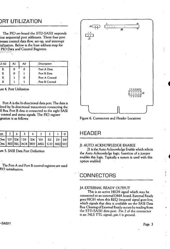
Figure
6.
Connectors and Header LocationsHEADER
]l
AUTO ACKNOWLEDGE ENABLE•
j I is the Auto Acknowledge Enable which selects
the Auto Acknowledge logic. Insertion of a jumper
enables this logic. Typically a system is used with this •
option enabled
CONNECTORS
JA EXTERNAL READY OUTPUT
This is an active HIGH signal which may be connected to an external DMA board External Ready goes HIGH when th is REQ (request) signal goes low, which signals that data is available on the SASI Data
Bus. Clearing of External Ready occurs by reading from •
. the STD·SASli data port. Pin 2 of the connector
is an 74LS TTL signal; pin I is ground. '
.,
JB SASI BUS
Figure 7 shows the symbol, direction and func-tion of the pins of JB, the 50-pin connector for the SASI Bus. The odd pins (I, 3, 5, ... ) are all grounded, the even pins active or unused. Interconnect is made typically with a 50-pin ribbon cable.
Pin No. Symbol ! Direction Function
2 DBO
I
,
Bi-directional Data Bit 0 4 OBI Bi·direcrional Data Bit I 6 DB2 Bi-directional Data Bit 2 8 DB3 Bi-directional Data Bit 310 OM Bi-directional Darn. Bit-4
12 DB5 Bi-direc'tional Data Bit 5
14 DB6 Bi-directional Data Bit 6 16 DB7 1 Bi-directional Data Bit 7
18
'N/C
! --20
N/C
!
-
-Z2
N/C
:-
-Z4
N/C
i
-
-26
N/C
I
.-
-28
N/C
i
,
-
-30
N/C
,
I-
-32
N/C
I
-
.-34
N/C
I ,i
-
-36 BSY Input Controller Busy 38 ACK Output . Request Acknowledge 40 RST
,
Output Reset Controller42 MSG I
Input Complete Message
44 SCL.
I
Output Select Controller46 ClD ! I· Input Comm.1ndlDatn Mode 48
REQ
J
Input Request Acknowledge 50. vo
!
Input Data DirectionFigure 7. SASI
Bus
Signal DefinitionsSTD-SAS11
-
,
'SPECIFICATIONS
o
System clock: 4.0 MHzo
Data Bus: 8 bits, bi-directionalo
Address Bus: 16 bitso
Signal Loading: Inputs: One 74LS maximumOutputs: IOH='-3mA min @
2.4 volts
. IOL =24mA @ 0.5 volts
o
Operating T emperatute:O°C
to60°C
o
System Interrupt Units: 1 SIUo
Interrupts: All three ZSO modeso
Power Requirements: @ 25· CParameter ~ Condition , Min. : Typ. i Max. : Units
Vee
, -
4.75 5.0 .5.25 ' Volts Icc @5.0V-
355 : 600 rnAMECHANICAL
o
Card Dimensions:Form Factor ,H W ,L i Units
STD-Bus 0.60 4.5 .6.5 1 inches
.0
PC Board thickness: 0.062 incheso
Connectors:STD-Bus UI): 56-pin dual readou~ 0.12 inch
•
centers •
SASI Bus UB): 50 pins; 0.100 inch centers Ext Ready UA): 2-pin; 0.100 inch centers
[image:6.602.42.544.28.851.2],
•
Q
U
"
C~
«
•
'"
oja:
•
!
0 I£1
.
g
0·
~
I
"- i!
01'
\
~
...
1 gV)
i
,~
,
«
i
~
V) 0,
'
, ,
f- !~ ! !
i
CI V) •
f
U~
31
I
•
N
:;
•
A
,
,
•
(
;;
~
~
rl'
!I
!
I
!
ti
iii •,
.
~
:f-'!t-
"
~~!-
u\~r
8n):;
t•
.
-
.
;
(~51
4
P
';i
,.'>
.
=
..
!
-1.1,1.1
.~·A
cA
~1J
~I~ ~ ~ ~
.
;/
,
~!
~" :> :IIU.U.U'
.~,
~ :
.
..
-
.
1~
~.
... !'-
.
0~ '
-
.-" f - ~ r-. ' ,
.
>-•
t.~~~j
~.
,;
,
l
I~!
•
•i<
~~,
•
,
l,!! a;il:.
•,
3;~
~
514
.
~ .-;,
•
..
.
"
.I~·
of" " ' ; :
I-;.!L
~a
D~~"~
.. : iii ;."
;.~
;
~-~
.. ".: I
d,
.
'I~·
Il! ii ! ~ .~~
-,
:II
:~
I~
Ii!~
;
I:
i
•
! \~=(10"'!"~2'CU)
:;
..
..
Q
,
•
!
!
I
•
~ ~N
"
•
0
•
•
~2 •
~~
"·
l!-F
-•
!
11
.
•
.~ ~ ei[
:;,.... 0
-~ <
"r
-•
•
; ~
..
- 0 •
"- r
~
~ <> co
I I I
,
o
CD
....,
r-;.
~
~
~L,
u
u
:I:
"'
,
..
«
....,
..
..
!
g
I
<Jl«:
~
<Jl I 0
I-a
<Jlu~
~
~0
i
<;> jO
~
,?
~
.
\
of
j •
I
i
j
.
.
...
11~ 3i
•
1
1=
I
g
0:"· a
•
N