Theoretical analysis of GaAs/AlGaAs
quantum dots in quantum wire array for
intermediate band solar cell
Sogabe, T, Kaizu, T, Okada, Y and Tomic, S
http://dx.doi.org/10.1063/1.4828359
Title
Theoretical analysis of GaAs/AlGaAs quantum dots in quantum wire array
for intermediate band solar cell
Authors
Sogabe, T, Kaizu, T, Okada, Y and Tomic, S
Type
Article
URL
This version is available at: http://usir.salford.ac.uk/37366/
Published Date
2014
USIR is a digital collection of the research output of the University of Salford. Where copyright
permits, full text material held in the repository is made freely available online and can be read,
downloaded and copied for noncommercial private study or research purposes. Please check the
manuscript for any further copyright restrictions.
intermediate band solar cell
Tomah Sogabe, Toshiyuki Kaizu, Yoshitaka Okada, and Stanko Tomi
Citation: Journal of Renewable and Sustainable Energy 6, 011206 (2014); doi: 10.1063/1.4828359
View online: http://dx.doi.org/10.1063/1.4828359
View Table of Contents: http://scitation.aip.org/content/aip/journal/jrse/6/1?ver=pdfcov
Published by the AIP Publishing
Articles you may be interested in
Effect of spacer layer thickness on multi-stacked InGaAs quantum dots grown on GaAs (311)B substrate for application to intermediate band solar cells
J. Appl. Phys. 111, 074305 (2012); 10.1063/1.3699215
Publisher’s Note: “Structural atomic-scale analysis of GaAs/AlGaAs quantum wires and quantum dots grown by droplet epitaxy on a (311)A substrate” [Appl. Phys. Lett. 98, 193112 (2011)]
Appl. Phys. Lett. 99, 139901 (2011); 10.1063/1.3633014
Structural atomic-scale analysis of GaAs/AlGaAs quantum wires and quantum dots grown by droplet epitaxy on a (311)A substrate
Appl. Phys. Lett. 98, 193112 (2011); 10.1063/1.3589965
Intermediate-band material based on GaAs quantum rings for solar cells
Appl. Phys. Lett. 95, 071908 (2009); 10.1063/1.3211971
Absorption characteristics of a quantum dot array induced intermediate band: Implications for solar cell design
Theoretical analysis of GaAs/AlGaAs quantum dots
in quantum wire array for intermediate band solar cell
Tomah Sogabe,1Toshiyuki Kaizu,1Yoshitaka Okada,1and Stanko Tomic´2,a)
1
Research Center for Advanced Science and Technology, The University of Tokyo, 4-6-1 Komaba, Meguro-ku, Tokyo 153-8904, Japan
2
Joule Physics Laboratory, School of Computing, Science, and Engineering, University of Salford, Manchester M5 4WT, United Kingdom
(Received 31 May 2013; accepted 1 August 2013; published online 12 November 2013)
A GaAs quantum dot (QD) array embedded in a AlGaAs host material was fabricated using a strain-free approach, through combination of neutral beam etching and atomic hydrogen-assisted molecular beam epitaxy regrowth. In this work, we performed theoretical simulations on a GaAs/AlGaAs quantum well, GaAs QD and QD array based intermediated band solar cell (IBSC) using a combined multiband
kp and drift-diffusion transportation method. The electronic structure, IB band dispersion, and optical transitions, including absorption and spontaneous emission among the valence band, intermediate band, and conduction band, were calculated. Based on these results, maximum conversion efficiency of GaAs/AlGaAs QD array based IBSC devices were calculated by a drift-diffusion model adapted to IBSC under the radiative recombination limit. VC 2013 AIP Publishing LLC.
[http://dx.doi.org/10.1063/1.4828359]
I. INTRODUCTION
Intermediate band solar cells (IBSC) concept have recently drawn a lot of attention, due to the reported high conversion efficiency of 63% under radiative recombination limit and maxi-mum light concentration.1,2 In order to reach this theoretical efficiency limit, the optimal loca-tion of the intermediate band (IB) between the valence band (VB) and conducloca-tion band (CB) of the host materials is required to be EgðVB;CBÞ ¼1:9 eV and EgðIB;CBÞ ¼0:7 eV. To date, a great number of material combinations have been employed to fabricate IBSCs. Among them, self-assembled InAs quantum dot (QD) arrays fabricated by molecular beam epitaxy (MBE) have been widely studied as a building block to create the IB in the GaAs host material. However, the band gap combination and the location of IB in InAs/GaAs QD based IBSCs is not favourable and the upper limit efficiency is around 20% (1 sun) and 34% (1000 suns).3–7In order to improve the IBSC efficiency, host materials with much wider band gap such as AlGaAs or GaP are required. Recently, we have succeeded in the fabrication of GaAs QD arrays embedded in AlGaAs quantum-wire (QWR) host material by using a combination of neutral beam etching and atomic hydrogen-assisted MBE regrowth.8 This top-down lithography and etching method is a strain-free approach, with the advantages of being able to precisely control the size, spacing, and arrangement of the QD during growth, which is difficult to achieve by self-assembling growth. In this study, we performed theoretical simulation of GaAs/AlGaAs QD arrays using a combined multi band kp and drift-diffusion transport method. The electronic structure, IB band dispersion, and optical transitions, including absorp-tion and spontaneous emission among the VB, IB, and CB, were calculated. Based on these pa-rameters, the theoretical conversion efficiency limit of GaAs/AlGaAs QD array based IBSC devices were calculated by a drift-diffusion model adapted to IBSC.9–11
a)
Electronic mail: [email protected]
II. THEORETICAL MODEL
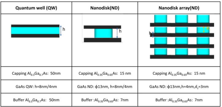
The QD array model considered here consists of GaAs QDs. As shown in Fig. 1, in order to better simulate the realistic, experimentally grown, structures, we have used the experimental results for structural parameters. A GaAs quantum well embedded in an Al0.3Ga0.7As matrix was used as a control sample. For the QD array, we have chosen a QD of height 4 nm, with vertical spacing set to dz ¼3 nm. The quantum mechanical description of the IBSC was based on the solutions of the Schr€odinger equation, H^kpwnðrÞ ¼EnwnðrÞ, with multi-band kp
Hamiltonian
^
Hkp¼
p2 2m0
þVðrÞ þh
2
k2 2m0
þhkp
m0
þ 1
4m2 0c2
½r rVðrÞðkþpÞ þDeeþVPZðeÞ; (1)
where the first term is the electron kinetic energy of the unperturbed system, the second is the potential due to QD shape and band edges of the QD or bulk material, and the rest are perturba-tive elements: the kinetic energy, coupling between zones in the system (thekp term), the spin orbit split off energy, the Pikus-Bir strain Hamiltonian, and the piezoelectric potential, respec-tively. The whole Hamiltonian, H^kp, is expanded using only the s-anti-bonding and px, py, pz
-bonding orbitals, all spin degenerate, into so called the 8-bandkpHamiltonian. The wave func-tions, wnðrÞ, are expanded into the plane-wave basis, jkþKi ¼eiðkþKÞr, where K is the wave
vector of the QD array, in order to provide the periodic boundary conditions suitable for the anal-ysis of such structures. More details about methodology can be found elsewhere.11,13
From the kp calculation, we obtained the position of EL, EH, and information about the density of states of NV B, NCB, and NIB. With the energy levels and wave functions, following the dipole approximation, the absorption coefficient is given as
aðhxÞ ¼ pe
2
c0m2 0nxX
X
K
X
i;f
jhij^e pðKÞjfij2d½EfðKÞ EiðKÞ hxðfiffÞ; (2)
where his the reduced Planck constant, xis the photon frequency, e is the electron charge, n is the refractive index, 0 is the dielectric permittivity of a vacuum, c is the vacuum speed of light,Xis the volume of the structure, ^eis the unit vector of light polarization, andpðKÞis the momentum operator. The optical dipole matrix element is given by hij^epðKÞjfi, and varies inside the Brillouin zone (BZ) of an QD array.9 The initial and final state energies are EiðKÞ
[image:4.612.126.488.539.715.2]andEfðKÞ, which also vary throughout the QD array BZ, hxis the photon energy, and fiðfÞ is the initial (final) state Fermi-Dirac distribution function.
The characteristic function for a QD of arbitrary shape, R, can be expressed in reciprocal space as12–14
vðkÞ ¼ 1 ð2pÞ3
ð
R
expðikrÞdr: (3)
The disk like shape of the QD in a quantum wire structure, used in our analysis, in the recipro-cal space suitable for modelling periodic arrays becomes
vdiskðkÞ ¼ 2pi kjjkz
½eikzH1DJ
1ðkjjDÞ; (4)
where kjj¼kxx^þky^y is the in-plane wave-vector, kz the wave-vector in the z-direction, J1 is the Bessel function of the first kind, andD andH are the diameter and height of the quantum nano-disk, respectively.
III. RESULTS
A. Band edge profile of GaAs/AlGaAs QD
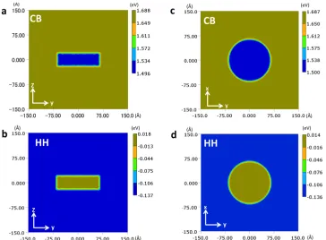
Figure 2 shows the two dimensional band edge profile of the GaAs/AlGaAs QD, with
[image:5.612.125.489.436.704.2]D¼15 nm and H¼4 nm. In the simulation we have used a shape function, Eq. (4), in recipro-cal space to describe the QD geometric structure. Figure 2shows the CB and heavy hole (HH) band edge profile of the GaAs QD projected in the xy-plane (c,d) and yz-plane (a,b). The num-ber of Fourier components was set as Nx¼Ny¼Nz¼50. The CB band edge is found at around 1.688 eV with the band offset CB¼0.19 eV, as shown in Figures2(a)and2(c). The HH edge is located at 0.018 eV with HH¼0.137 eV. These values are fairly close to the preset CB edge value 1.678 eV with CB¼0.16 eV and HH edge value 0.0 eV with HH¼0.124 eV.
FIG. 2. Band edge profile for GaAs QD: (a) CB edge profile inyzplane, (b) HH band edge profile inyzplane, (c) CB edge profile in xy plane, (d) HH band edge profile in xy plane. The Fourier components used in the simulation are
Nx¼Ny¼Nz¼50.
B. Electronic and optical properties of GaAs QW and GaAs QD
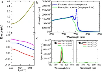
Figure3(a)shows the subband dispersions, along in-plane wave-vectorkjj, of the GaAs QW embedded in Al0.3Ga0.7As barrier material. The well width is 4 nm. It can be clearly seen here that nonparabolic (warping) subband dispersion curves exist in the valence band, which reflects the band mixing behavior in quantum wells due to the strong coupling between heavy-hole (HH), light-hole (LH) and spin-orbit split-off (SO) subbands in the VB. The valence band mixing has a profound impact on the calculation of the absorption or gain spectrum in a quantum well. Figure
3(b) shows the absorption spectrum calculated between the optically allowed transitions of CB and VB. In order to fit the experimental results, we have also calculated the absorption spectra under a two-dimensional exciton model.
The spontaneous emission spectrum was calculated using the following formula:15–18
RspðEÞ ¼ 8pnE
2
h3c2
1
eEkBTDF1
aðEÞ; (5)
wherehis the Planck constant, cis the speed of the light in a vacuum, nis the refractive index of GaAs, a(E) is the absorption coefficient, Eq. (2), kB is the Boltzmann constant, T is the temperature, and DF is the separation of the quasi-Fermi levels. The key step to calculate spontaneous emission is to accurately determine the DF. Near the BZ center, a parabolic band approximation is valid for QW. Meanwhile, if assuming that electrons occupy the ground state of both CB and VB, the injected carrier density can be expressed as,
Ne¼ ðmkBTÞ=ðph2LQWÞln½1þeðFcECB1Þ=kBT. Here, LQW is the QW width, m is the electron effective mass, and the quasi-Fermi level for electron, Fc, can be calculated as
Fc¼ECB1þkBTðeNeLQW=Ns1Þ, where Ns¼ ðmkBTÞ=ðph2Þ. The quasi-Fermi level for hole,
[image:6.612.126.487.442.697.2]Fv, can be determined similarly as Fv¼EHH1kBTðeNhLQW=Ns1Þ. Due to negligible differ-ence between perpendicular and in-plane electron effective mass in GaAs, we adopted the effective bulk mass m¼0:067m0.19,20 For a doped material, the charge neutrality relation
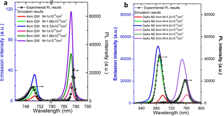
Nh¼NeþNAND holds and for an undraped QW,Nh is simply equal to Ne. In our simula-tion, we have examined three different carrier sheet densities:Ne¼11018, 1:661018, and 2:331018 cm2. Taking Ns¼21011 cm2 for the 4 nm wide GaAs QW structure, we can obtain the following values for DF: 1.65 þ 0.034 eV, 1.65 þ 0.102 eV, and 1.65 þ 0.311 eV for the three sheet densities, respectively. Assuming a finite broadening in the density of states of the QW, the final spontaneous emission spectrum is obtained, as shown in Figure3(c). It is found here again that the TM polarization gives rise to weak emission spectra. This can be quantitatively explained by the shape anisotropic effect of the wave function in the QW. Fitting of experimental PL data is plotted in Figure4(b). The emission spectra, including both TE and TM polarization, were averaged by (2TEþTM)/3. The simulation and experimental results are consistent to each other. The slighter larger value of FWHM (full width at half maximum) is due to the larger broadening factor used in the simulation and can be effectively tailored to match the experimental results. We also plotted experimental and simulated results for the QW with 8 nm width for better comparison.
In order to compare with the experimental PL results, we carried out a detailed calculation of the spontaneous emission spectra of the GaAs QD. Similar to the QW case, separation of quasi-Fermi levels DF¼FcFv has to be estimated first. The quasi-Fermi levels for electron
and hole in GaAs QD is determined by the following formulae:16
n2D¼
2N2D QD H
ð1
0 1 ffiffiffiffiffiffi 2p
p
rc
eðEECB1Þ2=2r2c 1
1þeðEFcÞ=kBTdE; (6)
p2D¼
2N2D QD H
ð1
0 1 ffiffiffiffiffiffi 2p
p
rv
eðEEHH1Þ2=2r2v 1
1þeðEFvÞ=kBTdE; (7) whereN2D
QD is areal density of GaAs QDs and n2Dand p2D are the electron and hole
concentra-tion normalised by the QD height, H. In order to better simulate the experimental results, we have taken the inhomogenous broadening effect due to the size fluctuations of the QDs into consideration. Carrier distribution is described by a Gaussian function centered at the discrete energy levelsECB1 andEHH1 with FWHM denoted as rc andrv, where rc is much larger than
rv due to large effective mass in VB (hererc¼0:025 eV and rv¼0:0012 eV). Ifn2Dandp2D
[image:7.612.127.488.529.716.2]are known, quasi-Fermi levels Fc and Fv can be determined from formulae Eqs. (6) and (7). Standard numerical simulation methods such as Newton-Raphson iteration are not suitable here. However, a simple “graphical method,” by plottingn2D orp2D as a function ofFcor Fv, can be used to determine the value of Fc andFv. Fig. 4(b) shows the simulated spontaneous emission
results along with the experimental PL results. From experimental fabrication conditions, we obtain the areal density of GaAs QD as 51010 cm2. We have chosen three different electron concentrations:n3D¼3:21018 cm3, 4:01018 cm3, and 5:91018 cm3. The temperature
was set at 30 K. It is found that at an electron concentration of 4:01018 cm3, corresponding quasi-Fermi level separation is in good agreement with the experimental PL results.
C. GaAs QD array based IBSC device simulation
Figure 5 shows the device structure for the GaAs QD based IBSC. We have adopted a
[image:8.612.126.485.98.262.2]pin structure where in the i region, ten layers of GaAs QD were embedded in the Al0.3Ga0.7As barrie material. Band edge profile is presented in Figure 5(b). In order to obtain miniband information due to the vertical coupling of the ten-layer GaAs QD, we have per-formed band dispersion calculations assuming periodic boundary conditions. The initial struc-ture simulation parameters were presented in Figure 1(see the QD array). Compared to a QD of width 8 nm, the wave function in QD of with 4 nm shows a stronger tendency to delocalize. FIG. 5. Device structure model (left) and Poison equation derived potential profile (right) for AlGaAs/GaAs/AlGaAs
pinsolar cell device.
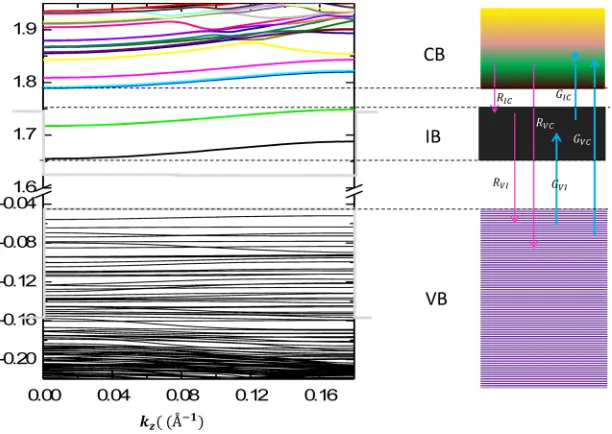
[image:8.612.154.460.490.707.2]We therefore chose GaAs QD, of width 4 nm in the array simulation. Band dispersion along wave vector Kz is presented in Figure 6. It can be seen that the band dispersion in VB is fea-tureless due to the large effective mass of holes (HH, LH) which flatten the band dispersion. In contrary, we found two minibands in CB, labeled, e1 and e2. Each has band width around 45 meV. However, since the band gap between these two bands is less than 25 meV, these two mini-bands are treated as one band by taking thermal fluctuation at room temperature (300 K) into consid-eration. A sketch of the band model for VB and IB is CB is plotted in the right side of Figure6. After having obtained band width and positions, we calculated the optical absorption coefficients
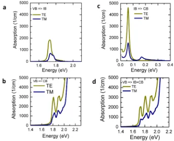
av;i,ai;c, andav;c for the three transitions: VB!IB, IB!CB, and VB!CB, respectively, which
are shown in Figure7. We also calculated the absorption spectrum from VB! ðCBþIBÞ, which is shown in Fig. 7(d). This transition accounts for the case where the quasi-Fermi level in IB is not separable from CB. In this case, we need to treat the IB and CB as one band. It should be noted that the broadening parameter has a strong effect on the magnitude of absorption coefficients. As we have mentioned before, the QD array studied here was fabricated using a top-down lithography and etching method, the advantage of which is the high accuracy in QD size control. Therefore, we used a fairly small broadening width of 10 meV in the absorption coefficient calculation.
All information obtained from the electronic structure calculations were used with the drift-diffusion model, adapted for a IBSC. The main contents of the IBSC drift-drift-diffusion model are given as follows.21–23 The generation rate of electrons per unit surface area from a band i to a band f higher in energy is denoted by Gif. The recombination rate of electrons per unit surface area from a bandf to a bandilower in energy is denoted by Rif. For the intermediate band to be in equilibrium, the net result of all the transitions into and out of the band must be zero, i.e.,
Gv;iRv;iþRi;cGi;c¼0. Once a system that is in steady state is found, the corresponding
cur-rent out of the conduction band can be evaluated: J¼eðGv;cþGi;cRi;cRv;cÞ. The flux of
[image:9.612.133.476.438.716.2]photons per unit solid angle from a blackbody would be given by Planck’s law if in a vacuum. We however will carry out all our analysis inside the cell, a material of refractive indexn^, which due to Snell’s law requires a different angular dependence. Inside a material of refractive index,
FIG. 7. Optical absorption coefficients for (a) VB to IB, (b) VB to CB, and (c) CB to IB transitions. We also calculated the continuous absorption from VB to (IBþCB), as shown in (d).
the flux of photons per unit surface area, per unit solid angle, in the range E!EþdE from a blackbody at temperature Tis given as/ifdE¼ ð2n2=h3c2ÞðE2=eE
=kBT1ÞdE. In this model, we assumed non-overlapping, constant, absorption coefficients aif. This means that the flux of
pho-tons able to cause a transition between any two energy levelsiand fis given by
Uif ¼ 2n
2
h3c2 ðEhigh
Elow
E2dE
ekBTE 1
; (8)
whereElowis the energy gap corresponding to the transition i!f andEhigh is the next lowest energy gap. The flux from the sun is received outside the material up to an anglehs at a
tem-perature of 6000 K, and for angles larger than this the flux is received from the surroundings at a temperature of 300 K. These angles must be converted using Schnell’s law to angles inside the materialhs andhc (critical angle of total internal reflection). Now, if we consider a point a
distance z from the surface of the solar cell, the generation follows Beer-Lambert’s law but with two terms, one taking into account photons reflected off the back of the solar cell. However, the optical path traveled to our point clearly has an angular dependence, and so the generation rate per unit volume,gif involves an integral overh,
gif ¼2p
ðhc
0
UifðhÞaif exp aif z
cosh
þexp aif
2Wz
cosh
" #
coshsinhdh: (9)
The angular dependence of UðhÞ takes care of the fact that some radiation comes from sun, 0<h<hs and some from the ambient surroundingshs<h<hc. The rate per unit surface area
is found by integrating overz, so that for a solar cell of widthW,Gif ¼Ð0Wgifdz.
This model differs from the traditional approach to the intermediate band solar cell by allowing both the absorption coefficients and the filling of the inter-mediate band to vary. They are coupled by assuming the absorption coefficients depend linearly on the carrier density in the intermediate band, i.e., aic¼ricnib, avi¼rviðNibnibÞ, where ric is the absorption cross
section for the transition,nibis the electron concentration in the IB, andNibis the density states in the IB. This is to say that the absorption coefficient into the IB is proportional to the concen-tration of empty states there, and the absorption coefficient out of the IB is proportional to the concentration of electrons in there.
The net rate rif of electrons per unit volume, per unit solid angle, de-excited from a band f
to a band of lower energy i whilst radiating into the same energy range of photons, which drives the corresponding absorption, is given by the generalised Planck formula,
rif ¼aif
2n2
h3c2 ðEhigh
Elow
E2dE
e
ðElifÞ
kBT 1
; (10)
wherelif ¼FfFi is the difference in energy of the Fermi levels, and Tis the temperature of
the solar cell, i.e., 300 K. Due to total internal reflection, this radiation can only escape the cell if it is emitted within a cone of semi-anglehc, the critical angle of total internal reflection,
ei-ther towards the front surface of the cell or the back surface of the cell (from which it will reflect). Since this emitted radiation may stimulated transitions along this optical path and be reabsorbed, we find an expression for the effective recombination rate per unit volume,
qif ¼2p
ðhc
0
rifðlifÞaif exp aif z
cosh
þexp aif
2Wz
cosh
" #
coshsinhdh: (11)
We note that rifis angular independent and the rate per unit surface area is again found by the integral,Rif ¼Ð0Wqifdz.
In the steady state relevant for SC operation, @=@t¼0. We adopt the charge conservation rulenþnibpþNþd ¼0, whereN
þ
have assumed that all donor atoms are ionized. The concentrations n, p, and nib are given by the relevant Fermi-Dirac distributions: n¼Nc=½eðEcFcÞ=kBT1, p¼N
v=½eðFvEvÞ=kBT1, and
nib ¼Nib=½eðEiFiÞ=kBT1, where Nc, N
v, and Nib are the effective density of states in the re-spective band.
For a current extracted from the solar cell at voltage V, the split between the valence and conduction band Fermi-levels in electron-volts is equal to that voltage, i.e., FcFv¼eV.
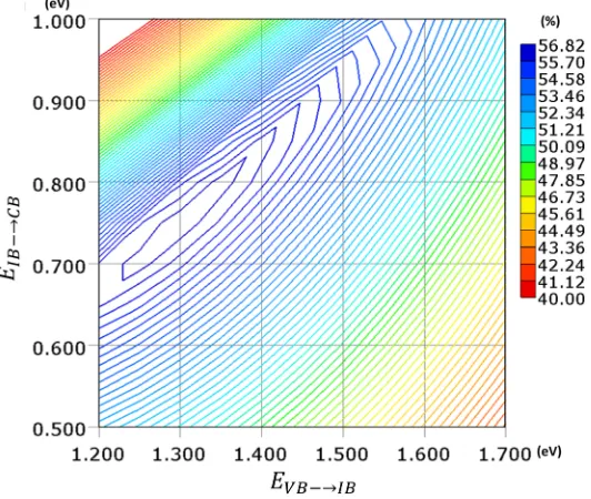
Figure8shows the efficiencies contour plot of a pre-filled IBSC with filling factor of 0.5 under light concentration of X¼1000 suns. At the subband gap combination ofEgðVB;IBÞ ¼1:3 eV, and EgðIB;CBÞ ¼0:74 eV, a maximum efficiency of 57% is obtained. This value is slightly lower than the detailed balance limit because of the limited device thickness (here 5lm). Setting the thickness large enough and under maximum concentration, we obtained exactly the 63.2%, the idealised efficiency value reported before.
Next, we performed efficiency calculations for the GaAs QD using the density of states, absorption coefficients, band width and location obtained by multiband kp calculation. The results are shown in Figure 9. Under the radiative recombination limit, we obtained 22.3% for a GaAs QD array based IBSC under 1 sun. Under 1000 suns, the efficiency can reach 33%. In Figure9, the current density plotted on the x-axis has been normalized by the concentration ra-tio,X, and is expressed asJ/X. In a conventional single junction solar cell, the short circuit cur-rent under concentration has the relation, JscðXÞ ¼XJsc (1 sun), thus J/X is constant and equal toJsc(1 sun). However, as can be seen in Figure9, for IBSC, the relation of JscðXÞto X is non-linear and the ratioJ/X is increases with increase of X, until saturation at large X. In our recent work, we have demonstrated that the nonlinear relation betweenJsc(X) and X is one crucial fin-gerprint to evaluate the carrier dynamics via IB for IBSC serving under light concentration.24 Effect of non-radiative transition like electron-phonon interaction or Auger effects11,25 on the efficiency of such QD in QWR structures is yet to be examined both experimentally and theoretically.
[image:11.612.175.441.492.717.2]In addition, it should be noted that the efficiency for a GaAs/AlGaAs QD is much lower than the ideal IBSC efficiency of 47% under 1 sun and 63% under full sun. This is due to the fact that the location of the IB in the current case is not optimal and the IB here is functioning as a recombination centre rather than an extra carrier generation centre. However, if we choose an appropriate material combination in order to create IB in the optimal position between CB and VB, the efficiency will be greatly improved and will approach the ideal value. One feasible
FIG. 8. Conversion efficiency contour map of IBSC calculated using the drift-diffusion model including the photofilling effect in IB. The contour plotted the relation by varying the energy separation between VB!IB and IB!CB.
solution is to replace the GaAs QD with a lower band gap material such as InGaAs to lower down the position of the IB. Although there exists some issues such as lattice mismatch, using the lithographic and etching methods developed in our group will greatly reduce the difficulties as one need only to control the epitaxial growth of InGaAs QW/AlGaAs.
IV. CONCLUSIONS
In conclusion, we have simulated an IBSC made of a GaAs QD array embedded in AlGaAs barrier material by combining a multiband kp and drift-diffusion model adapted for IBSC. Detailed calculations of the optical absorption and spontaneous emission of both GaAs QW and GaAs QD were performed and the results were in good agreement with experimental photoluminescence results. Using a drift diffusion model adapted for IBSC, we obtained con-version efficiency of 22.3% for a GaAs QD based IBSC under 1 sun and 33% under 1000 suns. The efficiency will be effectively improved by replacing the GaAs QD with a lower band gap material so as to lower the position of IB.
ACKNOWLEDGMENTS
The authors are grateful to the New Energy and Industrial Technology Development Organisation (NEDO), Japan, for financial support under grant: Research and Development on Innovative Solar Cells: Post-Silicon solar cells for ultra-high efficiencies. S.T. also wishes to thank the Royal Society, London, grant High Performance Computing in Modelling of Innovative Photo-Voltaic Devices, to the STFC e-Science, UK, for providing the computational resources and to M. Lundie for useful discussions.
1
A. Luque and A. Martı,Phys. Rev. Lett.78, 5014 (1997).
2A. Luque, A. Martı, and C. Stanley,Nature Photon.6, 146 (2012). 3
R. Oshima, A. Takata, and Y. Okada,Appl. Phys. Lett.93, 083111 (2008).
4
A. Luque, A. Martı, C. Stanley, N. Lopez, L. Cuadra, D. Zhou, J. L. Pearson, and A. McKee,J. Appl. Phys.96, 903 (2004).
5S. M. Hubbard, C. D. Cress, C. G. Bailey, R. P. Raffaelle, S. G. Bailey, and D. M. Wilt,Appl. Phys. Lett.92, 123512
[image:12.612.177.440.94.337.2](2008).
6
S. Blokhin, A. Sakharov, A. Nadtochy, A. Pauysov, M. Maximov, N. Ledentsov, A. Kovsh, S. Mikhrin, V. Lantratov, S. Mintairov, N. Kaluzhniy, and M. Shvarts,Semiconductors43, 514 (2009).
7
S. Tomic´, T. Sogabe, and Y. Okada, “In-plane coupling effect on absorption coefficients of InAs/GaAs quantum dots arrays for intermediate band solar cell,” Progress in Photovoltaics (submitted).
8
T. Kaizu, Y. Tamura, M. Igarashi, W. G. Hu, R. Tsukamoto, I. Yamashita, S. Samukawa, and Y. Okada,Appl. Phys. Lett.101, 113108 (2012).
9
S. Tomic´, T. S. Jones, and N. M. Harrison,Appl. Phys. Lett.93, 263105 (2008).
10R. Strandberg and T. W. Reenaas,J. Appl. Phys.105, 124512 (2009). 11
S. Tomic´,Phys. Rev. B82, 195321 (2010).
12
A. D. Andreev, J. R. Downes, D. A. Faux, and E. P. O’Reilly,J. Appl. Phys.86, 297 (1999).
13
S. Tomic´, A. G. Sunderland, and I. J. Bush,J. Mater. Chem.16, 1963 (2006).
14S. Tomic´, P. Howe, N. M. Harrison, and T. S. Jones,J. Appl. Phys.99, 093522 (2006). 15
E. Zielinski, F. Keppler, S. Hausser, M. H. Pilkuhn, R. Sauer, and W. T. Tsang,IEEE J. Quantum Electron.25, 1407 (1989).
16
S. L. Chuang,Physics of Photonic Devices(John Wiley and Sons, 2009).
17J. Kim and S. L. Chuang,IEEE J. Quantum Electron.42, 942 (2006). 18
S. Tomic´, E. P. O’Reilly, R. Fehse, S. J. Sweeney, A. R. Adams, A. D. Andreev, S. A. Choulis, T. J. S. Hosea, and H. Riechert,IEEE J. Sel. Top. Quantum Electron.9, 1228 (2003).
19
A. Danicic´, J. Radovanovic´, V. Milanovic´, D. Indjin, and Z. Ikonic´,J. Phys. D: Appl. Phys.43, 045101 (2010).
20D. Timotijevic´, J. Radovanovic´, and V. Milanovic´,Semicond. Sci. Technol.27, 045006 (2012). 21
L. Cuadra, A. Martı, and A. Luque,IEEE Trans. Electron Devices51, 1002 (2004).
22
M. J. Keevers and M. A. Green,J. Appl. Phys.75, 4022 (1994).
23
A. Luque, A. Martı, N. Lopez, E. Antolın, E. Canovas, C. Stanley, C. Farmer, and P. Dıaz,J. Appl. Phys.99, 094503 (2006).
24
T. Sogabe, Y. Shoji, M. Ohba, K. Yoshida, H.-F. Hong, C.-H. Wu, C.-T. Kuo, S. Tomic´, and Y. Okada, unpublished results (2013).
25
S. Tomic´, A. Marti, E. Antolin, and A. Luque,Appl. Phys. Lett.99, 053504 (2011).