International Journal of Emerging Technology and Advanced Engineering
Website: www.ijetae.com (ISSN 2250-2459, ISO 9001:2008 Certified Journal, Volume 6, Issue 7, July 2016)
72
To Improve Noise by Reducing Rise Time, Fall Time for
Dynamic CMOS Logic with Stack Techniques
Mayura Upasani
1, Sachin Bandewar
2Abstract:- The most common way to decrease noise is to add one or more stack transistors to the system. This decreases charge sharing and charge leakage problem and thus decreases noise problem. Stack transistors or transistor stacking has proven to be exceedingly most effective in reducing and minimizing sub threshold leakage or charge leakage in stand by mode of operation of circuit. It has been observed that this technique of using stack transistors saves around 33% in total leakage in 50nm devices. Dynamic CMOS circuits are extensively used in high performance Very Large Scale Integrated systems (VLSI). Conversely they undergo commencing limitations like noise tolerance, charge leakage, charge sharing, delay etc. Because of growing impact of process variations on design performance, belligerent technology scaling noise in dynamic CMOS has become than essential challenge. Noise is basically result of charge sharing problem and thus charge leakage problem. The noise stimulate in circuit would affect the performance of circuit, which should be so improved for reliable operation of VLSI systems.
Keywords-- Micro wind 3.0.
I. INTRODUCTION
There are several techniques that reduce the rise time, fall time and output current or fan-out in efficient way but the disadvantage of each technique that limit the switching speed and fan-out. Due to this there are so many limitations are occurs. In this dissertation we had use stack techniques that can improved switching response and fan-out.
For the calculation of rise time, fall time and delay time of the any CMOS logic circuit we are using computer simulation as well as analytical techniques.
Whenever we are using more complex CMOS logic circuit then we are considering appropriate transistor model for the simulation of Dynamic CMOS logic circuits.
The propagation delay tp of a gate defines how quickly it responds to a change at its inputs, it expresses the delay experienced by a signal when passing through a gate. It is measured between the 50% transition points of the input and output waveforms as shown in the figure for an inverting gate.
τp=( τpHL+ τpLH) / 2 eq.(1)
The τpHL defines the response time of the gate for a low to high output transition, while τpLH refers to a high to low transition. The propagation delay τp as the average of the two
1.1.1 Quick Design
International Journal of Emerging Technology and Advanced Engineering
Website: www.ijetae.com (ISSN 2250-2459, ISO 9001:2008 Certified Journal, Volume 6, Issue 7, July 2016)
73
V50% = VOL +(VOH-VOL)/2V50%=(VOH+VOL)/2 eq. (2)
V90% = VOL + 0.9(VOH-VOL) eq. (3)
V10% = VOL +0.1(VOH-VOL) eq.(4)
The τpHL defines the response time of the gate for a low to high output transition, while τpLH refers to a high to low transition. The propagation delay τp as the average of the two
1.1.2 Rise and Fall Times
Figure shows the familiar CMOS inverter with a capacity load CL that represents the load capacitance (input of next gates, output of this gate and routing) Of interest is the voltage waveform Vout(t) when the input is driven by a step waveform, Vin(t) as shown in figure
The equivalent circuits that illustrate the above behaviour are show in figure
Saturated : VOUT > VDD – Vt
Non-saturated : 0 < VOUT < VDD – Vtn
II. MOTIVATION
CMOS Technology was one of the main streams of VLSI Design. In 50nm and above technology switching speed is one of the main factors of system response. But when technology feature size shrinks switching speed create major issues. If we are design a small circuit with the help of CMOS design then switching speed cannot create major problem but when we are design a complex circuitry then switching speed cerate major problem.
For the solution of this problem we can used a technique that is called Stack technique. Through this we can improve the Switching speed or response of design circuitry. This technique is also used to reduce leakage current that can improve static power also.
Problem’s Formulation
There are certain issues of process variations, timing, noise tolerance, and power which are looked into together for operation optimization [2]. We will use stack technique to improve following aspects:-
Improve Rise time, Fall time, charge sharing, charge leakage problem in dynamic CMOS circuits.
Optimize dynamic CMOS circuits with MOSFET-based keepers to enable and improve the rise time, fall time and output current etc, when we equate them to their initial performances.
Background Work
International Journal of Emerging Technology and Advanced Engineering
Website: www.ijetae.com (ISSN 2250-2459, ISO 9001:2008 Certified Journal, Volume 6, Issue 7, July 2016)
74
Here we analyse previous technique that primarily target for reducing rise time, fall time and increasing fan-out. These techniques are shown in below. The approaches that are adopted in VLSI design. Hear we are using source voltage using NMOS, source voltage using PMOS, Feedback Keeper and Pre-charge internal nodes.III. METHODOLOGY
The most common way to decrease noise is to add one or more stack transistors to the system[12]. This can solve rise time, fall time and fan-out problem. Using faster flip-flops decreases the setup (tsu) and hold times (Vth) of the flip-flop, which in change decreases the time window that the flip-flop is vulnerable to Noise. When the input frequency is less, the chances of the input turning during the setup and hold time studied for their optimization using the ac small-signal frequency-domain analysis. To date, simulations and ensuing analyses for the Noise problem have been performed mostly in the time domain. Designers of digital systems has time and again confronted with the problem of Noise. The problem could be rectified by the effective use of stack transistors.
Dynamic Logic
In static logic families the pull up and pull down networks operate concurrently. Dynamic logic on the other hand uses a sequence of pre-charge and conditional evaluation phases which are controlled by the clock to realize complex logic functions. A dynamic logic block is shown in Figure. Both forms of Figure 4 can be used. In our analysis we will concentrate in Figure n-logic network. The operation of the pull-down network (PDN) can be divided into two major phases. The pre-charge and the evaluation phase. In what mode the circuit is operating is determined by the signal φ, the “clock” signal.
Propose Stack Method
In stack technique, MOS transistor is divided and stacked into two half width size transistors. When two half size stacked MOS transistors are turned off together, it induces reverse bias between them which results in the reduction of sub threshold leakage power. However, with increase in the number of transistors overall propagation delay of the circuit increases [12]. Using CMOS technology is basically for consuming less power. In this design criterion it focuses on sub threshold leakage power consumption and it also focuses on body biasing effect and stack effect. One of the main contributors for the static power consumption is sub threshold leakage current which is shown in the Figure i.e., the drain to source current when the gate voltage is smaller than the threshold voltage. As the technology feature size shrink sub current is increases exponentially as the decrease of threshold voltage. Stacking transistor can reduce sub-threshold leakage. So it is called stacked effect. Where two or more stacked transistor is turned off together, the result can reduce the leakage power.
International Journal of Emerging Technology and Advanced Engineering
Website: www.ijetae.com (ISSN 2250-2459, ISO 9001:2008 Certified Journal, Volume 6, Issue 7, July 2016)
75
Working PrincipalIn working principal, we solve all 8 cases and give their output with designed circuit. Here we are using 7-NMOS (3-7-NMOS with W and 4-7-NMOS with W/2),1-PMOS,3-source voltage and 1-LED. In circuit diagram red colour indicate high voltage or 1, brown colour indicate hold circuit and blank colour indicate low voltage or 0.
Case 1 :-
When we are taking CLK=0, A=0 and B=0 then circuit give high or 1 output
Case 2:-
When we are taking CLK=0, A=0 and B=1 then circuit give high or 1 output.
Case 3:-
When we are taking CLK=0, A=1 and B=1 then circuit give high or 1 output.
Case 4:-
International Journal of Emerging Technology and Advanced Engineering
Website: www.ijetae.com (ISSN 2250-2459, ISO 9001:2008 Certified Journal, Volume 6, Issue 7, July 2016)
76
Case 5:-When we are taking CLK=1, A=0 and B=0 then circuit is in hold mode.
Case 6:-
When we are taking CLK=1, A=0 and B=1 then circuit is in hold mode.
Case 7:-
When we are taking CLK=1, A=1 and B=0 then circuit is in hold mode.
Case 8:-
When we are taking CLK=1, A=1 and B=1 then circuit give high or 0 output.
International Journal of Emerging Technology and Advanced Engineering
Website: www.ijetae.com (ISSN 2250-2459, ISO 9001:2008 Certified Journal, Volume 6, Issue 7, July 2016)
77
IV. FUNCTIONAL SIMULATION
4.1 Software Used
Software used For CMOS layout design is micro wind 3.0.
4.2 Microwind Layout
Integrated Circuit (IC) Layout or mask design is the description of an integrated circuit in terms of planar geometric shapes which correspond to the patterns of metal, oxide, or implementation with enough information to deduce all the relevant physical parameters of the circuit. A layout engineer„s job is to place and connect all the components that make up a chip so that they meet all criteria. Typical goals are performance, size, and manufacturability. MICROWIND supports both end and back-end design flow. In order to design front-end, we use the Digital schematic editor i.e. DSCH which has simulator used for simulating digital circuits.
MICROWIND generates an error free CMOS layout, and if any error occurs it reminds the user about the occurrence of error.
Digital schematic editor could convert the digital circuits into Verilog file which may be moreover synthesized for FPGA/CPLD devices of any trafficker.
Micro wind‟s version 3 also supports the back end design.
In distinguishable Verilog file is compiled for layout conversion in MICROWIND.
In Micro wind, the CMOS layouts could be demonstrated using inbuilt mix-signal simulator and analyzed further for DRC, delays, 2D cross section, 3D view and etc.
4.2 (a) Layout of Propose Stack Method
Firstly, we can draw propose stack circuit in DSCH screen. For this we can used 2-PMOS, 7-NMOS, 1-Supply, 1-Ground, 1-Butten, 1-LED, and connecting wire that can used to give proper connection. Through this we can design propose stack circuit. After the completion of design it save in MSK format. Now, we are open Micro wind screen and open saved file. It can generate Lay-out of design circuit, after simulation it can plot graph between:-
Layout.
Voltage Vs Time graph.
Voltage Vs Current graph.
Frequency and Time graph.
This is the layout of designed proposed method. This proposed circuit diagram is design in DSCH and layout is generated through microwimd. Here we are using microwind 3.0 software.
This is the simulation of proposed method which are generated through microwind software. This simulation shows all inputs and output wave and their relations. Here we are giving all input variable wave form.
International Journal of Emerging Technology and Advanced Engineering
Website: www.ijetae.com (ISSN 2250-2459, ISO 9001:2008 Certified Journal, Volume 6, Issue 7, July 2016)
78
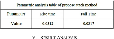
Parametric analysis table of propose stackFor the solution of this problem we can used a technique that is called Stack technique. Through this we can improve the Switching speed or response of design circuitry. This technique is also used to reduce leakage current that can improve static power also. Through this table we can give the value of rise time, fall time and output current. This table also shows that the stack technique improves the Rise time and fall time.
V. RESULT ANALYSIS
After implementing certain methods, we have found that stack method has proven to be enhancing current, decreasing rise time and fall time, Further it has found that delay is also reduced compared to other techniques.
Comparative Result Analysis
As we have compared different techniques of decreasing elements malfunctioning circuits like noise, charge leakage, charge sharing & delay. The comparison is shown in table 5.2. The comparison has clearly proved that proposed logic has proven advanced than other ones.
Comparative Parametric analysis table
In this table we are giving rise time and fall time values for all previous approaches and proposed stack technique. Through this table we compare all values of rise time, fall time and output current and says whose technique is best all of them.
VI. CONCLUSION
Through this technique we can improve rise time, fall time, and output current.
Future Scope
In this method we can improve the rise time, fall time and output current but here we can also increase the power dissipation that is the disadvantage of this method. So in future we can develop a new method that can overcome this problem. In other field work Noise is detected using 90nm technology and determining the various parametric estimations techniques for reducing power dissipation could be employed. The performance of the proposed Noise testing circuits should be improved, technique of improving power dissipation should be employed. With all the effects and errors cause due to scaling should be consider in the design of noise testing circuits ,design and optimization of systems using them.
The performances of the proposed Noise testing circuits should evaluate in terms of speed, area, and power and other stuck at faults.
With all non-ideal effects and soft errors cause due to scaling should be consider in the design of Noise testing circuits design and optimization of systems using them.
The responses from the tested devices were shown to correspond with simulation at lower clock frequency, below at higher clock frequency device is slower in the deep Noise region than it is in the deterministic region. Higher frequency MOSFET models require analysis of parasitic switching capacitances.
REFERENCES
[1] Hailong Jiao, Student Member, and Volkan Kursun publish their
paper on title "Reactivation Noise Suppression With Sleep Signal Slew Rate Modulation in MTCMOS Circuits" in IEEE transactions on Very Large Scale Integration (VLSI) systems, vol. 21, no. 3, march 2013.
[2] Kumar Yelamarthi, and Chien-In Henry Chen "Timing
[image:7.595.48.290.419.502.2]International Journal of Emerging Technology and Advanced Engineering
Website: www.ijetae.com (ISSN 2250-2459, ISO 9001:2008 Certified Journal, Volume 6, Issue 7, July 2016)
79
[3] Massimo Alioto,Gaetano Palumbo, and Melita Pennisi
"Understanding the Effect of Process Variations on the Delay of Static and Domino Logic" IEEE transactions on very large scale integration (vlsi) systems, vol. 18, no. 5, may 2010.
[4] Gaetano Palumbo, Melita Pennisi, Member. and Massimo Alioto
"A Simple Circuit Approach to Reduce Delay Variations in Domino Logic Gates" IEEE transactions on circuits and systems iregular papers, vol.59, no.10, october 2012.
[5] You-Gang Chen, I-Chyn Wey, and An-Yeu (Andy) Wu “A New
Noise-Tolerant Dynamic Circuit Design with Enhanced PDP Performance under Low SNR Environment” Graduate Institute of Electronics Engineering, National Taiwan University, Taiwan October 2012
[6] Farzan Fallah Fujitsu Labs. of America, Inc. Advanced CAD
Technology Group San Jose, California & Massoud Pedram University of Southern California Dept. of Electrical Engineering Los Angeles, California “Standby and Active Leakage Current Control” Los Angeles, California.
[7] H. Jiao and V. Kursun, “Ground-bouncing-noise-aware
combinational MTCMOS circuits,” IEEE Trans. Circuits Syst. I, Reg. Papers, vol. 57, no. 8, pp. 2053–2065, Aug. 2010
[8] P. Magnone, F. Crupi, G. Giusi, C. Pace, E. Simoen, C. Claeys, Fellow, IEEE, L. Pantisano, D. Maji, V. Ramgopal Rao, Senior Member, IEEE, and P. Srinivasan “1/f Noise in Drain and Gate Current of MOSFETs With High-k Gate Stacks”.
[9] You-Gang Chen, I-Chyn Wey, and An-Yeu (Andy) Wu Graduate
Institute of Electronics Engineering, National Taiwan University, Taiwan “A New Noise- Tolerant Dynamic Circuit Design with Enhanced PDP Performance under Low SNR Environment” [10] E-238 Analog VLSI Circuits Dr. Navakanta Bhat ECE department
Indian Institute of science Banglore 560012 August 2005.
[11] Razak Hossain “High Performance ASIC Design Using
Synthesizable Domino Logic in an ASIC Flow” Cambridge University Press.
[12] R.Divya, PG scholar, Karpagam University, Coimbatore, India.
NJ.Muralidharan M.E (Ph.D), Assistant Professor, Karpagam University, Coimbatore, India. “Leakage Power Reduction Through Hybrid Multi-Threshold C MOS Stack Technique In Power Gating Switch”
[13] Neil H.E. Weste, Kamran Eshragian Principles of CMOS VLSI
Design Second Edition, Pearson Education.
[14] Wikipedia, en.Wikipedia.org.
[15] P. Heydari and M. Pedram, “Ground bounce in digital VLSI
circuits,” IEEE Trans. Very Large Scale Integr. (VLSI) Syst., vol. 11, no. 2, pp. 180–185, Apr. 2003.
[16] A. Agarwal, D. Blaauw, and V. Zolotov, “Statistical timing
analysis for intra-die process variations with spatial correlations,” in Proc. ICCAD, 2003, pp. 900–907.
[17] K. Okada, K. Yamaoka, and H. Onodera, “A statistical gate-delay
model considering intra-gate variability,” in Proc. ICCAD, 2003, pp. 908–913.
[18] K. Okada, K. Yamaoka, and H. Onodera, “Statistical modeling of
gatedelay variation with consideration of intra-gate variability,” in Proc. ISCAS, 2003, pp. 513–516.
[19] J. W. Tschanz, J. T. Kao, S. G. Narendra, R. Nair, D. A.
Antoniadis, A. P. Chandrakasan, and V. De, “Adaptive body bias for reducing impacts of die-to-die and within-die parameter variations on microprocessor frequency and leakage,” IEEE J. Solid-State Circuits, vol. 37, no. 11, pp. 1396–1402, Nov. 2002.
[20] S. R. Nassif, “Modeling and forecasting of manufacturing
variations,” in Proc. ASP-DAC, 2001, pp. 145–150.
[21] W. Dai and H. Ji, “Timing analysis taking into account
interconnect process variation,” in Proc. IWSM, 2001, pp. 51–53.
[22] M.Orshansky, C.Spanos, and H.Chenming, “Circuit performance
variability decomposition,” in Proc. IWSM, 1999, pp. 10–13.
[23] I. Sutherland, B. Sproull, and D. Harris, Logical Effort. Designing
Fast CMOS Circuits. San Mateo, CA: Morgan Kaufmann, 1999
[24] S. Mutoh, T. Douseki, Y. Matsuya, T. Aoki, S. Shigematsu, and J.
Yamada, “1-V power supply high-speed digital circuit technology,” IEEE J. Solid-State Circuits, vol. 30, no. 8, pp. 847– 854, Aug. 1995.
[25] P. Larson and C. Svensson, “Noise in digital dynamic CMOS