© 2018, IRJET | Impact Factor value: 6.171 | ISO 9001:2008 Certified Journal | Page 269
DESIGN AND IMPLEMENTATION OF EFFICIENT ADDER USING VARIOUS
LOGIC STYLES
N.NAGARAJU
1, S.M.RAMESH
2,
SOUNDHARYA V
3, SOWMIYA K
41 Assistant Professor/ECE, Adhiyamaan college of engineering, Hosur, Tamil Nadu, India
2Professor/ECE, E.G.S pillay engineering college, Nagapattinam, Tamil Nadu, India
3,4ECE, Adhiyamaan college of engineering, Hosur, Tamil Nadu, India
---***---Abstract -In this paper, we present a comparison and study
of various adders. Adder's circuit is essential for designing various digital systems. The Complexity in VLSI design increases when the level of integration increases. In this paper, Adder is designed using a different technique which is based on MUX based adder, pass transistor, and logic 2-T logic. The efficiency of the system depends on the performance of internal components that are shown in the system. here, the internal components must be designed in such way that, they should consume less power with minimum time delay. The suggested circuit is better than the existing technique regarding area and delay. In several high-performance computing systems such as Digital Signal processors, FIR filters, Microprocessors, and Microcontrollers, the Multipliers are the key components where the adders are the basic building block. The design is targeted for the 0.18µm CMOS technology, and verification of the design is done by using TSPICE.
Index Terms: Adder, EDA tool, Multiplexer,
pass-transistor logic, 2-T logic
1.INTRODUCTION
In today's scenario, the demands of electronic devices are getting increased day by day. The use of portable electronic devices has been increased gradually[1]. The primary requirement of the portable electronic device is to reduce the power consumption and area and to increase the speed of operations. VLSI is a process where billions of transistors are embedded onto a tiny chip. The demand for the VLSI Designers is quite high for developing FPGA implementations, System on CHIP and ASIC. The Area along with minimum delay and power consumptions is one of the important design considerations for the IC designers in designing portable electronic devices and hardware circuits. The dependency of power consumption is based on the number of transistors used. The full adder[2] is one of the fundamental building blocks for many of the digital VLSI circuits. An adder is used to perform addition of numbers. In many computers and processors, adders are used in Arithmetic and Logic Units (ALU). They are also used in other parts of the processor, where they are used to calculate address table indices, increment and decrement operators and similar operations. A full adder has three inputs and two outputs which are A, B, C, SUM and CARRY.
The Logical circuit of this full adder can be implemented with XOR, AND and OR gates. The logic for sum involves XOR gate while the logic for CARRY involves AND and OR gates. The basic equation for SUM and CARRY of full adder is
SUM = A ⊕ B ⊕ C
CARRY = AB + BC + CA
[image:1.595.336.534.358.508.2]The logic diagram of the full adder using Boolean equations with basic gates can be represented as shown below.
Figure 1. Logic Circuit for Full Adder
The full adder[3] adds binary numbers and accounts for values carried in as well as out. The full adders are usually a component and cascade of adders, which adds 8, 16, 32, etc. bit binary numbers. The XOR gate is the basic element of any building block of the full adder concept. The performance of a full adder can be improved based on the performance of XOR gate. The previous designs of XOR gate were based on eight transistors or 6 transistors that are conventionally used in most of the designs. The main aim of reducing the transistor count is to reduce the size of XOR gate so that the maximum number of devices can be configured on a single silicon chip thereby reducing the area and delay. In the conventional full adder, two XOR gates are used whereas in the proposed method; we have used three different logic styles which are MUX based full adder which uses only one XOR gate, pass-transistor logic, and 2-T logic[5].
© 2018, IRJET | Impact Factor value: 6.171 | ISO 9001:2008 Certified Journal | Page 270 1.1 Proposed method
GDI Cell
[image:2.595.97.233.202.333.2]A Gate Diffusion Input [4]is a technique for low power digital circuit design in an embedded system. This technique is used to reduce power consumption, area, delay. This technique is used to reduce the number of transistors compared to conventional CMOS design.
Figure. 2.Basic GDI Cell
P G Out Function
0 B A AB F1
B 1 A A + B F2
1 B A A + B OR
B 0 A AB AND
C B A AB + AC MUX
0 1 A A NOT
Table 1 Boolean function of GDI cell
EXOR DESIGN USING GDI CELL:
When compared with other technologies GDI technology can reduce the number of transistor in this ex-or design.
Figure.3 EX-OR using GDI cell
Conventional MUX based full adder using GDI Cell:
To reduce the power and area, the conventional full adder in reduction phase of multiplier or any other processor is replaced by a modified full adder. The modified full adder circuits consist of 2:1 MUX and XOR gate. One XOR gate in the conventional full adder is replaced by a multiplexer block so that the delay path is minimized.
DELAY = XOR + MUX
[image:2.595.335.529.297.402.2]This can be implemented using second MUX with XOR output as a selection line. Since XOR involves most of the power consumption in adder circuits, by reducing the number of XOR gates power consumptions of the full adder can be reduced. This type of adder is employed in the multiplier, and so the efficiency is increased.
Figure 4. MUX Based Full Adder
The operation of adder is,
1. When both A and B are Zero or One, SUM = C,
2. When either of A or B is One, and another is Zero, SUM = C,
3. When both A and B are Zero or One, CARRY = A,
4. When either of A or B is One, and another is Zero, CARRY = C.
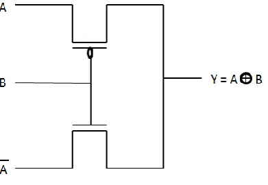
a) Pass Transistor Logic using GDI Cell:
In electronics, pass transistor logic describes various logic families used in the design of integrated circuits. Pass transistor logic is used to enhance the performance of arithmetic and logic circuits. This logic can be used to reduce the count of transistors used to make different logic gates by excluding redundant transistors.
[image:2.595.70.266.598.733.2]© 2018, IRJET | Impact Factor value: 6.171 | ISO 9001:2008 Certified Journal | Page 271 Figure 5. Pass Transistor Logic
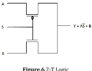
b. 2-T Logic using GDI Cell:
The 2-T logic[5] design which is a combination of both PMOS and NMOS. This logic is also known as CMOS logic. The 2-T logic is combined in a specific manner to get a full adder with SUM and CARRY output.
[image:3.595.315.553.357.510.2]This logic is very efficient when compared to MUX based full adder and pass transistor logic.
Figure.6.2-T Logic
1.1 Proposed method ripple carry adder-
In this paper, we have designed an 8-bit ripple carry adder using different logic styles such as pass transistor logic, mux-based logic, and 2T logic. An 8-bit ripple carry adder can be built by using eight 1-bit full adders. The Ripple carry adder creates a logic circuit using multiple full adders to add N-bit numbers.
Binary input A Binary input B Carry in
A0 00001111 B0
01010001 0
A1
00110011 B1 10010011 0
A2
01010101 B2 01010101 0
A3
10010011 B3 10101010 0
A4
10101010 B4 10010011 0
A5
01010101 B5 01010101 0
A6
10010011 B6 00110011 0
A7
[image:3.595.82.242.359.482.2]01010001 B7 00001111 0
TABLE 1. The truth table for Ripple Carry Adder (RCA).
The following truth table which consists of input from (A0-A7 AND B0-B7) the output (S0-S7) is as follows
[image:3.595.145.544.572.749.2]The above Figure shows the output for the first four inputs from a0 to a3 when added with the second four inputs b0 to b3 respectively.
© 2018, IRJET | Impact Factor value: 6.171 | ISO 9001:2008 Certified Journal | Page 272 The above Figure 9. shows the output for the first four inputs
from a4 to a7 when added with the second four inputs b4 to b7 respectively.
2. Performance Comparison:
Name Of The Design Number of
transistors Delay(ns)
Conventional MUX based full adder
(1-bit)
28 34.8
Proposed Pass Transistor
Logic (1-bit) 14 22
Proposed 2-T Logic (1-bit) 10 19
Conventional MUX based
RCA(8-bit) 224 32
Proposed Pass Transistor
RCA(8-bit) 112 24
Proposed 2-T RCA(8-bit) 80 22
The above table is used to compare the full adder designs that have been implemented using various logics. The various parameters such as some transistors and the time taken will be compared.
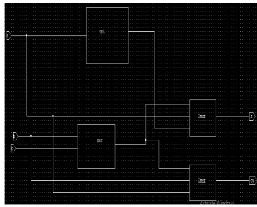
[image:4.595.308.564.80.265.2]3. Simulation Results:
[image:4.595.308.562.300.488.2]Figure 10. MUX based full adder design
Figure 10.1 MUX based full adder output
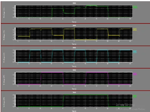
Figure 11. Pass transistor based full adder design
[image:4.595.47.276.387.542.2]Figure 11.1 Pass Transistor based full adder output
[image:4.595.304.559.521.726.2] [image:4.595.43.273.575.746.2]© 2018, IRJET | Impact Factor value: 6.171 | ISO 9001:2008 Certified Journal | Page 273 Figure 12.1 2-T full adder output
3. CONCLUSIONS:
In the project work, the full adder design is realized in three different logic styles with the help of MUX based full adder, pass-transistor logic, and 2-T logic. In this project work by using the obtained output for a 1-bit adder, the 8-bit adder has been designed and tested successfully, and the output is displayed. In the future, we will focus on various other logic designs which will provide a further improvement over various parameter and hence resulting in higher level of efficiency. The required logic can be realized within a smaller area when compared to the conventional full adder design. Simulation results show that this proposed full adder achieves better improvement regarding area and time delay when compared with other full adders.
REFERENCES:
[1] Hung Tien Bui, Yuke Wang, and Yingatao Jiang, "Design and Analysis of Low Power 10-Transistor full Adders Using Novel XOR-XNOR Gates", IEEE transactions on circuits and systems-ii: analog and digital signal processing Vol.49, No. 1, January 2002.
[2] Aditya Kumar Singh, Bishnu Prasad De, Santanu Maity, “Design and Comparison of Multipliers Using Different Logic Styles”, International Journal of Soft Computing and Engineering (IJSCE) ISSN: 2231-2307, volume-2, Issue-2, May 2012.
[3] Shen-Fu Hsiao, Ming-Roun Jiang, Jia-Sien Yeh, “Design of highspeed low-power 3-2counter and 4-2 compressor for fast multipliers”, IEEE Electronics Letters, 19th February 1998 Vol. 34 No. 4, ISSN: 0013-5194.
[4] Jashanpreet Kaur, Navdeep Kaur and Amit Grover “ A review on gate diffusion input(GDI)” in International Journal of Advance Research in
Electronics, Electrical & Computer Science Applications of Engineering & Technology Volume 2, Issue 4, July 2014, PP [385-391].
[5] N. Srinivasan Rao, B. Vijayasree, “Design the 2*1 MUX with 2T Logic and comparing the Power Dissipation and Area with different logics, “IJAREEIE, Vo1. 4. Issue 3, March 2015.