IMPLEMENTATION OF VISION-ASSISTED PATH PLANNING SYSTEM FOR BULK DIE SORTING IN SEMICONDUCTOR INDUSTRY
H.J. Yap1*, C. H. Ooi2 and S.W. Chang3
1Department of Mechanical Engineering, Faculty of Engineering, University of Malaya, Malaysia
2Department of Mechanical Engineering, Faculty of Engineering, University of Malaya, Malaysia
3Bioinformatics Programme, Institute of Biological Sciences, Faculty of Science, University of Malaya, Malaysia
ABSTRACT
Semiconductor integrated circuits (IC) are found in all of today’s electronic devices. Low cost mass production has enabled electronics to revolutionize the way people live and work. One major operation in IC assembly is die sorting, where individual die is categorized by grade. The traditional vision-assisted pick-and-place die sorting approach has high accuracy but low throughput. In this research, a bulk die sorting approach through vision-assisted path planning is studied and implemented. The objective of this system is to provide accurate die classification through vision processing and high die sorting throughput with efficient path planning. The system hardware consists of two parts, motion XY-stage used for wafer planar translation and optical unit used for acquiring wafer images. Firstly, the wafer image is acquired using the image mosaicing method. Then, die classification is performed to obtain the positions of functional and non-functional dies. Subsequently, point and coverage path planning algorithms are applied to determine the optimum path for physical die sorting operation. Overall, the proposed system showed significant improvement in the wafer image quality, low mismatch of dies, and obtained the shortest traversal time and distance for clustering dies by using the combined heuristic cluster with nearest neighbour algorithm. The system showed that the best coverage path planning method is the back-and-forth filling using decelerate-reaccelerate motion in terms of processing time (1.6 s), traversal time (137.2 s) and XY-stage stresses. As a conclusion, through the integrated implementation of hardware and software encompassing wafer image acquisition, die classification and path planning, the die sorting system is capable of achieving accurate die sorting with high throughput.
Keywords: die sorting, vision-assisted, path planning, semiconductor, bulk production
1 INTRODUCTION
Semiconductor manufacturing is a huge undertaking in terms of process steps and complexity. The entire manufacturing process involves upwards of 500 processing steps and takes up to 3 months to complete. The complexities involved include different chip types, package types, customer specifications and scale of integration. The processing steps can be broadly divided into 4 parts: wafer fabrication, wafer probing, device assembly and device testing [1]. The device assembly, also known as device packaging, can be further divided into multiple discrete steps: wafer dicing, wafer cleaning, die sorting, die attach, wire bonding, mould encapsulation, tin plating and lastly trim and form.
Die sorting is a major step in device assembly, which occurs after wafer dicing. It is the process of selecting and arranging the individual dies according to their grades [2]. This reduces waste from assembling sub-standard dies and assuring quality in the final product. The grade classification information is derived from wafer probing and wafer surface vision inspection. The information can be communicated either by black ink dots on the die surface or through inkless virtual wafer maps [3].
Traditionally, the die sorting step is combined with the die attach step. The vision and pick-and-place system would process each individual die in turn [4]. In order to cover all dies on the wafer, the back-and-forth scanning approach is used [5]. The process has high accuracy but low throughput as each die is processed independently. The die sorting process can be sped-up significantly by decoupling it from the die attach step. Instead of processing each die individually, dies on the wafer can be processed together as the inspection and sorting costs are high. In this study, a bulk die sorting approach through vision-assisted path planning is proposed. The proposed die sorting system is divided into three parts: wafer image acquisition, die classification and sorting path planning. In wafer image acquisition, super-resolution wafer images are acquired using the image mosaicing method with vision-motion correction. In die classification, image processing techniques are used to segment, interpolate and classify dies from the wafer image. In sorting path planning, the point path planning algorithms are used for individual die sorting whereas the coverage path planning algorithms are used for bulk die sorting.
2 MATERIALS AND METHODS 2.1 System Hardware
Semiconductor manufacturing at the leading edge of technology always require high speed and high accuracy of XY-stages in the range of microns for die bonding and wire bonding [6]. The mechanical XY-stage are motion stages that allow movement along the two major perpendicular axis (typically named X- and Y-axis), which is known as the serial structure. The other configuration is the parallel XY-stage where the mass and inertia is reduced [7]. The only drawback is limited stroke length. Besides that, precision XY Theta stages can also be found in industrial applications for high performance manufacturing [8].
The system hardware for the proposed die sorting system consists of motion XY-stage and vision optical system developed by a semiconductor industry. The motion XY-stage system is used for image acquisition and die sorting operation. It is a serially-connected linear XY-stage, driven by alternating current (AC) servo motors and controlled via computer. The motion hardware components and specifications are shown in Figure 1.
Figure 1: Motion Hardware Components
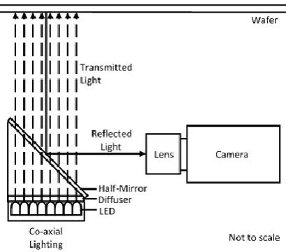
Figure 2: Vision Hardware Configuration 2.2 Wafer Image Acquisition
Image mosaicing is used for creating large composite images, typically in super-resolution from lower resolution images where there is a need for high resolution and large field of view [11-13]. In the image acquisition step, the complete wafer image with reference to the XY-stage coordinates must be captured. Image mosaicing technique is used here since a high resolution and large field of view image of the wafer is needed [11, 13]. The wafer's sub-segment images are taken in 2-dimension translational position offsets with overlaps between neighbouring images. Next, these sub-segment images are combined together to form a composite high resolution and large field of view image.
There is minimal information content in the repeating die patterns of the sub-segment wafer images. This limits the application of mosaicing algorithm [14]. As a result, offline vision-motion calibration is required to compensate for vision-vision-motion misalignment. The offline calibration step is used to overcome the rotation and shift deviations, which are the main errors in this type of image mosaicking [11]. At the start of die sorting, lighting intensity calibration and lighting uniformity calibration is performed. Next, online image acquisition and mosaicing are performed. At the start of each die sorting cycle, the wafer's sub-segment images are taken in fixed positions of the motion system. Up to 9 by 9 images are acquired in the X- and Y-direction to cover the complete wafer including overlap. The image acquisition pitches are calculated by using Equations (1)-(3).
#𝑖𝑚𝑎𝑔𝑒,𝑥 ≥
∅6-inch-wafer
𝐹𝑂𝑉𝑥 or #𝑖𝑚𝑎𝑔𝑒,𝑦 ≥
∅6-inch-wafer
[image:3.595.206.411.262.442.2]Assuming square active field of view,
#𝑖𝑚𝑎𝑔𝑒,𝑦= #𝑖𝑚𝑎𝑔𝑒,𝑥 (2)
𝑃𝑖𝑡𝑐ℎ𝑥 = 𝑃𝑖𝑡𝑐ℎ𝑦=
∅6-inch-wafer #𝑖𝑚𝑎𝑔𝑒,𝑥−1=
∅6-inch-wafer
#𝑖𝑚𝑎𝑔𝑒,𝑦−1 (3)
where,
∅6-inch-waferis the diameter of 6-inch wafer 𝐹𝑂𝑉𝑥 is the camera field of view in X direction 𝐹𝑂𝑉𝑦 is the camera field of view in Y direction
#𝑖𝑚𝑎𝑔𝑒,𝑥 is the number of images in X direction for acquisition #𝑖𝑚𝑎𝑔𝑒,𝑦 is the number of images in Y direction for acquisition 𝑃𝑖𝑡𝑐ℎ𝑥 is translational pitch for image acquisition in X direction 𝑃𝑖𝑡𝑐ℎ𝑦 is translational pitch for image acquisition in Y direction
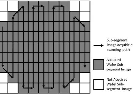
[image:4.595.182.398.389.541.2]Since the wafer is circular shaped, three images at each of the four corners do not contain wafer information, thus those images are not captured, leaving 69 sub-segment images required to cover a complete wafer. The image acquisition uses the back-and-forth filling method, scanning in the main X-axis from left to right, while moving back-and-forth along the Y-axis, as shown in Figure 3. During image mosaicing, the sub-segment images are first compensated for uniformity using the generated second-order polynomial curved grey surface image. Next, the sub-segment images are corrected in rotation and slant in order to correlate the vision system pixel positions to the motion system physical positions. Subsequently, the sub-segment images are tiled according to their relative 2D position and image pitch in pixels. This generates the final complete wafer image for the subsequent image processing step.
Figure 3: Wafer Sub-segment Image Acquisition Scanning Pattern: Back-and-Forth 2.3 Die Classification
Next, the die classification is performed. The functional die and ink die classification are performed based on the area hole and structure factor features. The maximum allowed area hole is used to define the largest dark patch on the die surface allowed and still remain as a functional die. This prevents miss-categorization due to minor stains on the die surface. Nonetheless, the maximum allowed area hole must be a value smaller than the smallest actual ink dot size, to prevent miss-categorization of actual ink dies as functional dies. Next, the structure factor feature was selected heuristically by comparing the list of available features between functional dies and ink dies. The structure factor feature is useful when the ink dot is off-centred, leading to a zero area hole.
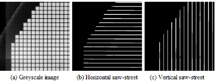
[image:5.595.124.489.375.518.2]For the non-functional dies interpolation, the wafer orientation and die pitch information are required. For wafer orientation, the dark saw-street regions are first segmented, but with grey level range between 0 and the next grey level histogram minima. Next, through the morphology erosion operator, the horizontal and vertical saw-street regions are selected using long rectangular erosion structure elements, as illustrated in Figure 4. Using the longest horizontal and vertical saw-street regions, the die pitch in the horizontal and vertical direction is determined through one-dimensional edge-pair measuring of the dies along the selected saw-streets. Using the die length, die width, die horizontal pitch, die vertical pitch and wafer orientation information, a 3 by 3 dies structure element is generated. The interpolated dies that do no intersect the functional dies and ink dies represent the non-functional pattern dies, edge dies and empty dies. All non-functional dies can be found by repeatedly executing the dilation operation until no new non-functional die is introduced. These regions are then passed to the path planning step for planning the transducer route for the physical die sorting operation.
Figure 4: Saw-street Segmentation 2.4 Path Planning
Path planning is important to minimize the travelling time and distance, which various optimization methods have been used in robotics and automation [17]. The physical die sorting operation is divided into two parts: individual die sorting and bulk die sorting. Individual sorting is used for high accuracy sorting, down to the single die control, which is suited for non-functional die sorting. In almost all cases, non-functional dies in a wafer occur in clustered but odd shapes, which require fine single die sorting capability. On the other hand, bulk sorting is used for high throughput sorting whereby the transducer is continuously scanned, which is suited for functional die sorting. In almost all cases, the functional dies in a wafer vastly outnumber the non-functional dies, hence requiring a faster sorting speed.
2.4.1 Point Path Planning
For individual die sorting of non-functional dies, the motion system XY-stage needs to move each non-functional die to the transducer for sorting operation to occur. This problem which is known as the Travelling Salesman Problem required both of the XY-stage travel distance and time to be minimized. The number of non-functional dies on a wafer can be in the thousands range, depending on the die size and wafer fabrication process. There are many approximate algorithms for the Travelling Salesman Problem in the literatures [18 & 19]. In this study, two algorithms which are heuristic cluster algorithm and nearest neighbour algorithm are tested and compared.
The heuristic cluster algorithm takes advantage of the concentrated spatial distribution of similar grade dies within a wafer [1]. Given a list of die positions, the adjacent dies are first clustered together to form die segments. The problem is then simplified to solving the Travelling Salesman Problem for traversing the die segments, instead of individual die positions. This greatly reduces the problem set size for the Travelling Salesman Problem. The nearest neighbour algorithm is a simple approximate algorithm for solving the Travelling Salesman problem [19]. It achieves local optimization of travel path, without regards to global optimality. The nearest neighbour algorithms work by selecting the initial XY-stage position as the first current position. Then, the nearest Euclidean distance position not yet visited is selected as the next current position. This is repeated until all die positions are traversed. The processing time and traversal time are measured using the computer's built-in time keeping system, as the point path planning algorithm is being executed and as the XY-stage is traversing the planned path during sorting. The travel distance (in mm) is calculated from the generated path distance (in pixels) using the distance per pixel ratio between the motion and vision system. The ratio used here is 45.7 μm per pixel.
2.4.2 Coverage Path Planning
The coverage path planning is used for high speed bulk functional die sorting. From the image processing die classification step, a coverage region is passed to the coverage path planning algorithm. The path planning algorithm is then used to find the shortest path to traverse the coverage region such that the transducer's contact area touches all points of the coverage region. Similar to the point path planning, the shortest traversal path in the coverage region problem would also lead to the shortest traversal time, which is important in this high speed, high throughput system. In the complete coverage problem, there are two main filling methods, which are back-and-forth [20] and spiral filling [21].
In order to investigate these two methods, a study is devised to check the processing time, traversal time, torque exerted and power drawn for the back-and-forth and spiral filling methods. In addition, two motions between straight line segments types are investigated: continuous motion and decelerate-reaccelerate motion. For continuous motion, the XY-stage does not decelerate, stop and reaccelerate between straight line segments. This motion is fast, but the XY-stage experiences stresses during direction change at sharp corners between straight line segments. In contrast, for decelerate-reaccelerate motion, the XY-stage decelerates, changes direction and reaccelerates between straight line segments. For this motion, the XY-stage experiences minimal stress during direction change at sharp corners between straight line segments. However, this comes at the expense of lower motion speeds. Data are collected for two different wafers.
3 RESULTS AND DISCUSSIONS 3.1 Die Classification
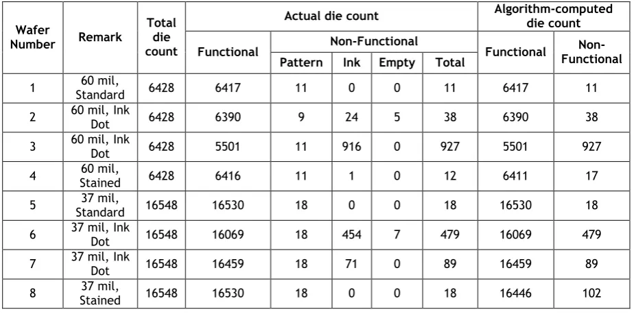
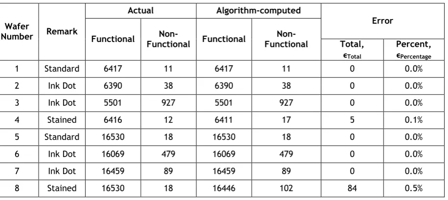
[image:7.595.77.541.266.495.2]The actual and algorithm-computed die classification count results are presented in Table 1. The die classification count is performed for 8 different wafers with different die sizes, functional die distribution, and die cleanliness. For actual die classification count, the non-functional die category is further divided into pattern die, ink die and empty die. From Table 1, 60 mil die wafers have a total die count of 6428 while 37 mil die wafers have total die count of 16,538. These total die count is consistent irrespective of method (actual or algorithm-computed), non-functional die distribution and wafer cleanliness. Besides that, the number of pattern dies for 60 mil and 37 mil die wafers are 11 and 18 respectively. For Wafer 2 (60 mil die size), the number of pattern dies is only 9 instead of 11, because the other 2 pattern dies are missing, and classified under the empty die label.
Table 1: Actual and algorithm-computed die classification count
Wafer
Number Remark
Total die count
Actual die count Algorithm-computed die count
Functional Non-Functional Functional Functional
Non-Pattern Ink Empty Total
1 Standard 60 mil, 6428 6417 11 0 0 11 6417 11
2 60 mil, Ink Dot 6428 6390 9 24 5 38 6390 38
3 60 mil, Ink Dot 6428 5501 11 916 0 927 5501 927
4 Stained 60 mil, 6428 6416 11 1 0 12 6411 17
5 Standard 37 mil, 16548 16530 18 0 0 18 16530 18
6 37 mil, Ink Dot 16548 16069 18 454 7 479 16069 479
7 37 mil, Ink Dot 16548 16459 18 71 0 89 16459 89
8 Stained 37 mil, 16548 16530 18 0 0 18 16446 102
Next, the error between the algorithm-computed and actual die classification count is presented in Table 2. The total error is presented as the absolute difference between the actual and algorithm-computed functional die count whereas the error percentage is presented as the percentage ratio of die count error to the actual total wafer die count. From the results, the error is zero for standard and inked dot wafers, for both 60 mil and 37 mil die size wafers. There is an error of 5 dies (0.1%) for Wafer 4 and 84 dies (0.5%) for Wafer 8. Both Wafer 4 and Wafer 8 are wafers with stains on the die surface. Nonetheless, in all cases, only the actual functional dies are misclassified as non-functional dies by the computing algorithm. None of the non-functional dies are misclassified as functional die.
3.2 Point Path Planning
produces the shortest traversal time for Wafer 3. The travel distance results showed a similar pattern as the traversal time.
Table 2: Error between algorithm-computed and actual die categorization count
Wafer
Number Remark
Actual Algorithm-computed
Error
Functional Functional Non- Functional Functional Non- Total,
ϵTotal
Percent, ϵPercentage
1 Standard 6417 11 6417 11 0 0.0%
2 Ink Dot 6390 38 6390 38 0 0.0%
3 Ink Dot 5501 927 5501 927 0 0.0%
4 Stained 6416 12 6411 17 5 0.1%
5 Standard 16530 18 16530 18 0 0.0%
6 Ink Dot 16069 479 16069 479 0 0.0%
7 Ink Dot 16459 89 16459 89 0 0.0%
8 Stained 16530 18 16446 102 84 0.5%
Table 3: Processing time for point path planning algorithms
Wafer Number
Number of non-functional Dies
Processing Time (s)
Default Heuristic Cluster Algorithm
Nearest Neighbour Algorithm
Combined Heuristic Cluster with Nearest Neighbour Algorithm
1 16 2.6 2.6 2.6 2.6
2 1064 2.5 3.7 2.5 3.7
[image:8.595.58.521.530.649.2]3 58 2.6 2.6 2.6 2.6
Table 4: Traverse time and distance for point path planning algorithms
Wafer Number
Number of non-functional
Dies
Default Heuristic Cluster Algorithm Neighbour Nearest Algorithm
Combined Heuristic Cluster with Nearest Neighbour Algorithm
Time Distance Time Distance Time Distance Time Distance
1 16 24.8 652.9 23.1 531.7 20.9 360.7 20.9 362.8 2 1064 899.1 16525.8 741.4 9941.8 615.5 3345.2 650.9 4267.1 3 58 54.1 1016.6 49.0 711.6 49.7 495.0 45.4 489.0
a smaller traversal time but greater travel distance than the nearest neighbour algorithm. Although not substantiated, this could be attributed to the several long travel distances between points for Wafer 3 using the heuristic cluster algorithm, which allows it to accelerate to higher speeds, hence reducing its traversal time. In contrast, most travel distance between points for Wafer 3 using the nearest neighbour algorithm are of moderate lengths. Overall, the nearest neighbour algorithm is the best point path planning algorithm for non-clustering non-functional dies whereas the combined heuristic cluster with nearest neighbour algorithm is the best point path planning algorithm for clustering non-functional dies
3.3 Coverage Path Planning
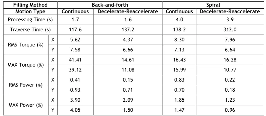
[image:9.595.76.537.290.492.2]The processing time, traversal time, RMS torque, MAX torque, RMS power and MAX power for coverage path planning algorithms using back-and-forth and spiral filling methods as well as continuous and decelerate-reaccelerate motion types are presented in Table 5, which is the average of two runs with different wafers. The RMS torque, MAX torque, RMS power and MAX power parameter values are given independently for the X and Y motor axis.
Table 5: Results for coverage path planning
Filling Method Back-and-forth Spiral
Motion Type Continuous Decelerate-Reaccelerate Continuous Decelerate-Reaccelerate
Processing Time (s) 1.7 1.6 4.0 3.9
Traverse Time (s) 117.6 137.2 138.2 312.0
RMS Torque (%) X 5.62 4.37 8.30 7.96
Y 7.58 6.66 7.13 6.64
MAX Torque (%) X 41.41 14.61 16.43 16.28
Y 39.12 11.08 15.99 10.77
RMS Power (%) X 0.41 0.15 0.83 0.22
Y 0.93 0.71 0.70 0.18
MAX Power (%) X 3.90 2.09 1.85 1.23
Y 4.05 1.50 1.47 0.96
From Table 5, the processing time for the coverage path planning using the spiral filling method (3.9s to 4.0s) is longer than the back-and-forth filling method (1.6s to 1.7s). Next, the traversal time for the decelerate-reaccelerate motion type is longer than the continuous motion type for both the back-and-forth and spiral filling method. Overall, the traversal time for the back-and-forth filling with continuous motion has the shortest traversal time of 117.6 seconds. This is followed by the back-and-forth filling with decelerate-reaccelerate motion (137.2s) and spiral filling with continuous motion (138.2s). The longest traversal time is produced by the spiral filling with decelerate-reaccelerate motion at 312.0 seconds.
The decelerate-reaccelerate motion is less useful for the spiral filling method because the spiral filling has fewer sharp changes in direction between its straight line segments, unlike the back-and-forth filling method. With respect to the continuous motion, the decelerate-reaccelerate motion reduces the RMS power and MAX power only slightly, but at the expense of a large increase in traversal time. This large increase in traversal time could be attributed to the many straight line segments approximated from the smooth continuous spiral path, which lead to increased decelerate and reaccelerate motion behaviour.
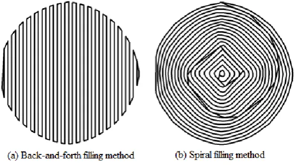
[image:10.595.141.435.265.429.2]The spiral filling is best coupled with the continuous motion whereas the back-and-forth filling is best coupled with the decelerate-reaccelerate motion. The spiral filling with the continuous motion method's good performance with short traversal time and moderate XY-stage stress agrees with the work by researchers [21-22]. Besides that, the back-and-forth filling with the decelerate-reaccelerate motion method also produces good coverage path planning performance. The graphical traversal path for Wafer 1 using back-and-forth and spiral filling methods is shown in Figure 5.
Figure 5: Coverage Path Planning Traverse Path for Wafer-1
Overall, the back-and-forth filling with decelerate-reaccelerate motion is the best coverage path planning algorithm investigated, in terms of processing time (1.6 s), traversal time (137.2 s) and XY-stage stresses (RMS torque: 4.37% (X), 6.66% (Y); MAX torque: 14.61% (X), 11.08% (Y); RMS power: 0.15% (X), 0.71% (Y); MAX power: 2.09% (X), 1.50% (Y)). The back-and-forth filling with decelerate-reaccelerate motion has an advantage over the spiral filling with continuous motion because it can accelerate to higher speeds along its long straight line segments to reduce traversal time and decelerate to lower speeds around sharp corners to reduce mechanical stresses.
4 CONCLUSION
5 ACKNOWLEDGEMENT
The authors would like to acknowledge the Ministry of Education of Malaysia for the financial support under the Fundamental Research Grant Scheme (FRGS), Grant No: FP061-2015A. The funders had no role in study design, data collection and analysis, decision to publish, or preparation of the manuscript.
6 REFERENCES
[1] Chen, J.C., Rau, H., Sun, C.J., Stzeng H.W., Chen, C.H. 2009. Workflow Design and Management for IC Supply Chain, International Conference on Networking, Sensing and Control (ICNSC), Okayama, Japan, 26-29 March, pp 697-701
[2] Wu, T., Li, B., Wang, L.W., Huang, Y. 2010. Study on Auto-path Planning According to Grade Priority for Sorting Dies. International Conference on Machine Learning and Cybernetics (ICMLC), Qingdao, China, 11-14 July, pp 1590-1595
[3] Wang, Z., Duan, H., Zhang, X. 2009. An Improved Greedy Genetic Algorithm for Solving Travelling Salesman Problem, Tianjin, China, 14-16 Aug, pp 374-378
[4] Medding, J., Stalder, R., Niederhauser, M., Stoessel, P. 2004. Thin Die Bonding Techniques. IEEE/CPMT/SEMI 29th International Electronics Manufacturing Technology Symposium, San Jose, CA. USA, 14-16 July, pp 68-73
[5] Wu, T., Li, B., Wang, L.W., Huang, Y. 2010. Automatic Detect and Match of LED Dies Basing on Position Relations between Adjacent Dies. International Conference on Machine Learning and Cybernetics (ICMLC), Qingdao, China, 11-14 July, pp 1195-1200 [6] Liang, J., Chen, J.Z., Zhang, Q., Kuang, Y., Zhang, X. 2012 A Novel XY-Theta Alignment
Stage for Screen Printing and Its Accuracy Analysis. International Conference on Mechatronics and Automation (ICMA), Chengdu, China, 5-8 Aug, pp 1352-1357
[7] Shen, J., Lou, Y. 2009. Topology Optimization of a Linear-Motor Actuated Parallel XY Stage, International Conference on Information and Automation (ICIA), Zhuhai, Macau, China, 22-24 June, pp 762-767
[8] Zhu, Y., Hu, C., Hu, J., Zhang, M., Xu, D. 2013. On-axis Self-calibration of Precision XY-θz Metrology Systems: An Approach Framework. IEEE/ASME International Conference on Advanced Intelligent Mechatronics (AIM), Wollongong, NSW, Australia, 9-12 July, pp 1078-1083
[9] Basler, A.G. 2010. User’s Manual For GigE Cameras. Retrieved from
http://www.baslerweb.com/media/documents/AW00089316000_ace%20GigE%20Users %20Manual.pdf
[10] Basler, A.G. 2011. The Elements of GigE Vision. Retrieved from
http://www.baslerweb.com/media/documents/GigE%20Vision%20White%20Paper.pdf
[11] Chen, F., Zhang, C., Shi, J., Chen, P. 2012. A New Method for Image Matching. 19th International Conference Mechatronics and Machine Vision in Practice (M2VIP), Auckland, New Zealand, 28-30 Nov, pp 190-193
[12] Huber-Mork, R., Soukup, D. 2009. Image Super-Resolution for Line Scan Cameras Based on a Time Delay Super-Resolution Principle. 6th International Symposium on Image and Signal Processing and Analysis (ISPA), Salzburg, Austria, 16-18 September, pp 129-134 [13] Nasibov, A., Nasibov, H., Hacizade, F. 2009. Seamless Image Stitching Algorithm using
[14] Steckhan, D., Paulus, D. 2010. A Quadratic Programming Approach for The Mosaicing of Virtual Slides that Incorporates the Positioning Accuracy of the Microscope Stage. Annual International Conference of the IEEE Engineering in Medicine and Biology Society (EMBC), Buenos Aires, Argentina, 31 Aug-4 September, pp 72-77
[15] Sahoo, P.K., Farag, A.A., Yeap, Y.P. 1992. Threshold Selection Based on Histogram Modeling. IEEE International Conference on Systems, Man and Cybernetics, Chicago, IL, USA, 18-21 Oct, pp 351-356
[16] Chang, H.T., Pan, R.J. 2012. Automatic Counting of Packaged Wafer Die Based on Machine Vision. International Conference on Information Security and Intelligence Control (ISIC), Yunlin, Taiwan, 14-16 Aug, pp 274-277
[17] Tahriri, F., Mousavi, M., Yap, H.J., Dawal, S.Z.D., Taha, T. 2015. Optimizing the robot arm movement time using virtual reality robotic teaching system. International Journal of Simulation Modelling. 14(1), pp 28-38
[18] Tsai, C.Y., Liu, C.H., Wang, Y.C. 2012. Application of Genetic Algorithm on IC Substrate Drilling Path Optimization. International Conference on Advanced Mechatronic Systems (ICAMechS), Tokyo, Japan, 18-21 September, pp 441-446
[19] Xiang, Z.Y., Gao, X.Y., Chen, Z. Y., Ouyang, L.B., Chen, D.L. 2010 Solving TSP Based on Multi-Segment Multi-Orientation Nearest Neighbor Algorithm. IEEE International Conference on Intelligent Computing and Intelligent Systems (ICIS), Xiamen, China, 29-31 Oct, pp 452-457
[20] Huang, W.H. 2001. Optimal Line-Sweep-based Decompositions for Coverage Algorithms. Proceedings of IEEE International Conference on Robotics and Automation (ICRA), Seoul, South Korea, 21-26 May, pp 27-32
[21] Lee, T.K., Baek, S.H., Oh, S.Y., Choi, Y.H. 2010. Complete Coverage Algorithm Based on Linked Smooth Spiral Paths for Mobile Robots. 11th International Conference on Control Automation Robotics & Vision (ICARCV), Singapore, 7-10 December, pp 609-614 [22] Surve, S., Singh, N.M., Lande, B.K. 2007. CPPA: A Fast Coverage Algorithm.