Design and Implementation of Area Efficient
BPSK and QPSK Modulators Based On FPGA
Akanksha Sinha1, Piyush Lotia2
1
M.E. Scholar [VLSI Design], Dept. of ETC, Shri Shankaracharya Technical Campus, Bhilai, Chhattisgarh
2
Associate Professor, Dept. of E&I, Shri Shankaracharya Technical Campus, Bhilai, Chhattisgarh
Abstract— Digital communications devices designed on FPGAs are capable of affording multiple communications protocols without the need to arrange new hardware, and can support new protocols in a matter of seconds. In addition, FPGAs provide a means to update systems that are physical difficult to access. For these reasons, FPGAs provide us with an ideal platform for implementing adaptive communications algorithms. This paper proposes a new approach to digital modulator techniques, applied to telemetry applications; simplifying the hardware design and inherently increasing data rate. This paper describes a method to implement modulation techniques (BPSK, QPSK and 8PSK) to transfer high data rate on field programmable gate array (FPGA). The implementation have been successfully done in VHDL using Xilinx ISE 13.2 Design suite and finally implemented in SPARTAN-3 FPGA.
Keywords— BPSK, QPSK, 8-PSK and FPGA
I. INTRODUCTION
Modulation is a method which is used to encode information from digital form to analog form. The digital modulation scheme is more secure and efficient for transmission as compared to other. The correction and noise detection are better in digital techniques over analog techniques. The selection of digital modulation scheme will significantly affect the characteristics and performance of a communication system. The objective of a digital communication system is to transport digital data between two or more nodes. This is usually achieved in radio communication by adjusting a physical characteristic of a carrier (sinusoidal), the frequency, phase, amplitude or a combination of it. This is performed in real systems with a modulator at the transmitting end to impose the physical change to the carrier and a demodulator at the receiving end to detect the resultant modulation on reception. Field-programmable gate arrays (FPGAs) are semiconductor devices containing programmable logic elements (LEs) and a hierarchy of reconfigurable interconnects to realize any complex combinational or sequential logic functions. Today’s FPGAs consist of configurable embedded static random-access memories (SRAMs), high-speed input/output (I/O) elements, high-speed transceivers and even hard-embedded processors. FPGAs are widely used in different applications, such as motor controllers, neural network implementations, finite-impulse-response (FIR) filter realization, fuzzy-logic controllers, etc. Also, FPGAs provide a means to update systems that are physical difficult to access. For these reasons, FPGAs provide us with an ideal platform for implementing adaptive communications algorithms. FPGA based design for QPSK & 8-PSK modulator implementation for satellite communication is given by Satish Sharma et al. [2]. Similar work has been proposed by Dhivya Jose, et al. [3] In which carrier waveform for the modulator generated using coordinate rotation digital computer CORDIC algorithm which uses shift, addition and very small look up table (LUT). [1] proposed BPSK and BFSK modulation techniques in low power consumption systems and for high speed systems. a novel design which contains minimum number of blocks necessary for designing of basic binary digital modulators and implemented on Altera DE2 FPGA Board is proposed by C. Erdogan et al [4], [8] published a study to develop an implementable low power QPSK modulator. [10] proposed a method to design BPSK modulator and Demodulator using Matlab/Simulink environment and implement it to FPGA Spartan 3E kit. [11] proposed a real time implementation of FPGA based frequency synthesizer by utilizing I/Q modulation. Many other researchers [5, 6, 7, 9, 12 and 13] have also focused on the development of on chip based communication system. Rest of this paper is as follows, section-II methodology for BPSK, QPSK and 8PSK modulator design, followed by simulation result in section-III, finally section-IV concludes this paper.
II. METHODOLOGY
A. BPSK- Modulator
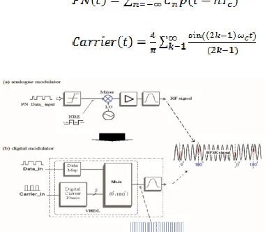
wireless communication. In wireless applications, such modulation may also be used for medical purposes, such as satellite telemetry, biotelemetry, telemedicine and healthcare. Furthermore, endoscopy, retina and brain telemetry devices are mainly developing with a high data rate. There is a high demand for a higher data rate, because of increasing the electrode numbers for reading the nerve signal information or controlling data. In such applications BPSK has advantages over FM, AM, ASK and FSK modulations. We propose in this section to develop VHDL code to generate a digital BPSK signal for improving modulator performance and increasing the data rate. Compared to the other analog modulators, this type of modulator provides digital synthesis and the flexibility to reconfigure and upgrade with the two most often used languages VHDL-and Verilog-based. The BPSK signal can be represented mathematically in equation (1), while the input data and transition for carrier wave is shown in Figure-1.
) (1)
[image:3.612.223.398.278.337.2]As revealed in Figure 1, the digital data is converted from analog or already generated in digital form and, this is required to convert to the analog modulator performance. For this technique, it is essential to convert the binary data m (t) into NRZ signal that maps the logic (0) to -1V (nominal) and logic (1) to + 1V. This data signal controls the transition shift (0), (π) for the carrier signal. That results in high power consumption for these types of analog modulators, reduces their efficiency and limits their biomedical application. This also increases the hardware complexity of the circuit and produces a large physical device.
Figure 1: BPSK waveform with respect to (NRZ) data state
The proposed modulator was developed with a VHDL description code to generate carrier shifts (0) and (180°) which are controlled by the input binary data to perform the transition of the BPSK signal. The modulator consists of digital and analog parts as shown in Figure 2. The proposed modulator output signal at multiplexer ( ) is in digital modulated form. It can be expressed as:
(2)
The filter is essential for the modulator to complete the process (off-chip); the output signal produced by the filter has an analog form. In this work, we investigated two types of filters, the first is low pass filter (LPF) and the second is band pass filter (BPF). The BPSK VHDL modulator output signal fed into the test filters.
Generally, the output is selected by the multiplexer then filtered with either a passive band pass filter or low pass filter to eliminate the high frequencies and the harmonics which are associated with the square wave signal, in order to provide the transmit analog signal (Tx). The simulated random data signal (Data_in) that is generated by a PN sequence can be represented by the Fourier series analysis as expressed in equation (3), where the input carrier signal is a periodic pulse train signal, which mathematically can be expressed in equation (4).
(3)
(4)
[image:3.612.215.405.532.698.2]The module system was synthesized with VHDL programming code and simulated with the Xilinx 13.2.
B. QPSK- Modulator
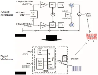
QPSK also one type of phase shift keying which is under the digital modulation. Demand for a high data rate for the data returned from the body is increasing, and require an efficient modulator to achieve both a high data rate and low power consumption. In such applications, the QPSK modulation has advantages over other schemes, and double symbol rate with respect to the BPSK over the same spectrum band. All analog or hybrid analog/digital QPSK modulators work with the phase shift of the carrier ( ), as the key of the modulation. The phase shifter is the most important element in the modulator to acquire two discrete signals sin( ) and cos( ). Practically, it uses a direct digital synthesizer (DDS) or numerical control oscillator (NCO) to generate the carrier signal. However, in analog modulation it is essential to use the NRZ format to map and, that produces analog QPSK signal, which can be represented mathematically in equation (5) and / are defined in equations (6) and (7) respectively:
(5)
(6)
(7)
Where: is the frequency carrier. is the in phase of data.
is the quadrature of data.
is the number of ( =2, marks this a BPSK, =4 is QPSK)
These types of conventional modulators are not suitable for medical applications, which are essentially working with the input data in NRZ signal form. The proposed QPSK modulator was programmed to generate a carrier phase shifter, to acquire four discrete states (0º, 90º, 180º, and 270 º), where the input data was split into two separate streams in-phase , and quadrature phase , to map the carrier signal, which was interfaced to the multiplexer.
The output is selected by multiplexer to provide a digital QPSK signal, which passes via a passive filter before being transmitted that eliminates the high frequencies. Figure 3 demonstrates the proposed VHDL QPSK modulator compared to an analog modulator. The digital QPSK signal of the multiplexer output can be represented in equation (8) below:
(8)
[image:4.612.225.385.577.699.2]To simplify the modulator design, the principle of the QPSK analog modulator, that is the main challenge for converting and designing the modulator in simple digital form. However, in analog modulation when generating the QPSK signal and data are in NRZ signal format, it is essential to map the data into I and Q streams, which are influence the carrier signal according to the transition of the input data. These types of techniques are not suitable for biomedical applications; it is conventional modulators, which are essential when working with the input data in NRZ signal format. To convert the carrier, it is synthesized with a periodic pulse signal, which generates four discrete states (0°, 90°, 180°, and 270°), whilst the data mapping is described in different concepts. Figure 4 describes the first concept (A). The direct digital modulator is controlled by two streams and Q of the carrier (0°, 270°) and inverted data is the controlling carrier (90°, 180°), then two carriers are combined together and subtracted in order to produce the QPSK signal. The critical point in this process is difficulty of converting the adder/subtractor in full design of modulator in digital form.
Figure 4: A Concept for generating direct QPSK digital modulator
C. 8-PSK Modulator
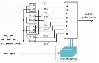
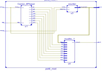
[image:5.612.237.378.317.355.2]The higher level of direct digital modulations is the 8-PSK. As a result of extending the symbol rate, the separation between phase states becomes smaller and susceptibility to noise increases. The 8-PSK modulator is described as deploying, the highest order PSK constellation. The challenge in digital modulation schemes is for a perfect synthesis design to minimize the processing circuit with compatible hardware. In practice, there are different topologies to synthesize the 8-PSK modulator, which is mostly used in mobile communication and in modern telecommunication. The modulator block diagram is shown in Figure-5, which is possible for synthesis with the FPGA technologies. The signal constellation usually deals with binary data that means the number of symbols, the symbols probabilities constellation diagram for the 8-PSK modulator as shown in Figure-6.
Figure-5: Block diagram for 8-psk modulator
Figure 6: Constellation diagram of 8-PSK modulator
Third proposed modulator is 8PSK, which is composed of eight discrete signals as (0°,45°, 90°,135°), (180°,225°, 270°, 315°). These carrier signals are controlled by the binary input data through a counter to generate (2 − 8 where = 3), that performs the transition of the eight carrier signals data mapping. It is then interfaced into eight inputs multiplexer, and the output provides an 8- PSK digital signal. However, we demonstrate in Figure 4.9, the principle of the proposed direct digital modulator 8-PSK. The multiplexer output for the digital 8PSK signal can be expressed in equation (4.9) below as:
[image:5.612.260.356.384.464.2](9)
Figure 7: Principle of direct digital modulator 8-PSK in FPGA/CPLD
[image:5.612.225.390.589.693.2]provides the essential transitions of the carrier. The multiplexer is a selectable switch which is interfaced from the carrier phase hifter and mapped data; the output provided is an 8-psk digital signal.
III.SIMULATIONRESULTS
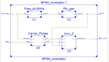
The new simple VHDL Binary Phase shift Keying (BPSK) modulator has been synthesized for transcutaneous biomedical devices applications. It is programmed with the Hardware Description Language (VHDL) code to generate the behavioural BPSK digital signal. The behavioural simulation (RTL view) for BPSK modulator is shown in Figure- 8 and the waveform simulation is presented in Figure-9.
[image:6.612.212.401.173.281.2]Figure8: RTL View for BPSK Modulator
Figure 9: Simulation Waveform of BPSK Modulator at clock size 100us
The behavioural simulation (RTL view) for QPSK modulator is shown in Figure-10 and the waveform simulation is presented in Figure-11 which demonstrates the output signal waveforms indicating the transitions (90°) ( 180°) of the carrier signal (output of multiplexer), due to the data influence.
[image:6.612.185.425.307.435.2]Figure 11: Simulation Waveform of QPSK Modulator with clock size 100us
[image:7.612.215.392.232.355.2]The behavioural simulation (RTL view) for 8-PSK modulator is shown in Figure-12 and the waveform simulation is presented in Figure-13 which demonstrates the transition of the digital signal for 8- PSK modulator output.
Figure 12: RTL View for 8-PSK Modulator
Figure 13: Simulation Waveform of 8-PSK Modulator at clock size 100us
TABLEI:COMPARISON OF DEVICE UTILIZATION FOR BPSK,QPSKAND 8PSKMODULATOR
Parameters BPSK QPSK 8-PSK
Selected Device Xc3s50-5pq208 Xc3s50-5pq208 Xc3s50-5pq208
No. of Slice 6 out of 768
0%
10 out of 768 1%
4 out of 768 0% No. of Slice Flip
Flops
10 out of 1536 0%
15 out of 1536 0%
7 out of 1536 0%
No. of 4 input LUTs 9 out of 1536 0%
17 out of 1536 1%
7 out of 1536 0%
No. of bonded IOBs 4 out of 124 3%
7 out of 124 5%
7 out of 124 5%
No. of GCLKs 1 out of 8
12%
1 out of 8 12%
[image:7.612.187.421.379.517.2] [image:7.612.120.491.556.724.2]IV.CONCLUSION
The digital modulators (BPSK, QPSK and 8PSK models) have been successfully designed, simulated and synthesized with VHDL programming code in Xilinx 13.2. The proposed work presented a better performance with high data rate. The output of the multiplexer produced a BPSK or QPSK digital (square) signal waveform with the data rate of 2Mbps with very low area requirement. Proposed technique simplifies the modulator to synthesize with FPGA or CPLD technologies, and useful for various applications. Synthesis report shows that our proposed design consumes lesser area while providing high data rates. Some other techniques of modulation can further be implemented through our proposed technique.
REFERENCES
[1] Mehmet SONMEZ1, Ayhan AKBAL “FPGA Based, Low Cost Modulators of BPSK and BFSK, Design and Comparison of Bit Error Rate over AWGN Channel” Gazi University Journal of Science GU J Sci 26(2):207-213, 2013.
[2] Satish Sharma, Sunil, Vijaykumar Pujari, Vanitha M, P.Lakshminarsimhan “FPGA Implementation of M-PSK Modulators for Satellite Communication” International Conference on Advances in Recent Technologies in Communication and Computing. 2010
[3] Dhivya Jose, Reneesh C Zacharia , Rijo Sebastian.” A Novel Approach For the Design and Implementation of FPGA Based High Speed Digital Modulators Using Cordic Algorithm” IJEDR | Volume 2, Issue 2 | ISSN: 2321-9939”, 2014.
[4] C. Erdoğan, I. Myderrizi, and S. Minaei, “FPGA Implementation of BASK-BFSK-BPSK Digital Modulators” Proceedings of the IEEE Antennas and Propagation Magazine, Vol. 54, No. 2, April 2014
[5] Oscar Jimenez, Oscar Lucia, LuisA.Barragan, Denis Navarro, Jose I. Artigas, and Isidro Urriza “FPGA-Based Test-Bench for Resonant Inverter Load Characterization” IEEE TRANSACTIONS ON INDUSTRIAL INFORMATICS, VOL. 9, NO. 3, August 2013
[6] Santa Concepcion Huerta, Angel de Castro, Member, Oscar Garcıa and Jose A. Cobos “FPGA-Based Digital Pulse width Modulator(DPWM) With Time Resolution Under 2 ns”, IEEE TRANSACTIONS ON POWER ELECTRONICS, VOL. 23, NO. 6, November 2008.
[7] Zdravko Lukic, Kun Wang, and Aleksandar ProdiC “High-Frequency Digital Controller for DC-DC Converters Based on Multi-Bit L A Pulse-Width Modulation” IEEE 2005.
[8] Asraf Mohamed Moubark, Hilmi Sanusi, Mohd Alauddin Mohd Ali and Sawal Md. Ali “FPGA Implementation of Low Power Digital QPSK Modulator Using Verilog HDL” Journal of Applied Science, 2013 ISSN 1812-5654/DOI:103923/jas.. Asian Network for Scientific Information , 2013.
[9] Zhu, Q.; Ma, R.; Duan, C.; Yamanaka, K.; Teo, K.H. “FPGA Implemented Multi-Level IFPWM Power Coding for Class-S PA in an All-Digital GHz LTE Transmitter” Mitsubishi Electric Research Laboratories, Inc.,201 Broadway, Cambridge, 2014
[10] S.O. Popescu, A.S.Gontean and G.Budura, “BPSK System on Spartan 3E FPGA”, SAMI 2012 • 10th IEEE Jubilee International Symposium on Applied Machine Intelligence and Informatics • January 26-28, 2012.
[11] Juha Suviola, Markus Allen, Mikko Valkama, and Markku Renfors “Real-Time FPGA Implementation And Measured Performance Of I/Q Modulation based Frequency Synthesizer” 19th European Signal Processing Conference, EUSIPCO 2011
[12] M. M. Ebrahimi, M. Helaoui, and F. M. Ghannouchi “Time-Interleaved Delta-Sigma Modulator For Wideband Digital GHz Transmitters Design And SDR Applications” Electromagnetics Research B, Vol. 34, 263-281, 2011
[13] Meng Li, Christophe Jego, Jianxiao Yang and Catherine Douillard “A Shuffled Iterative Bit-Interleaved Coded Modulation Receiver for the DVB-T2 Standard Design, Implementation and FPGA Prototyping”
[14] Anshul Agarwal, Student Member, IEEE and Vineeta Agarwal, Senior Member, IEEE “FPGA Realization of Trapezoidal PWM for Generalized Frequency Converter”
[15] K.Harikrishna, T. Rama Rao, Vladimir A. Labay “FPGA Implementation of FFT Algorithm for IEEE 802.16e (Mobile WiMAX)” International Journal of Computer Theory and Engineering, Vol. 3, No. 2, ISSN: 1793-8201, April 2013
[16] B.Sreedevi, V.Vijaya, Ch.Kranthi Rekh, Rama Valupadasu, B.RamaRao Chunduri, “FPGA Implementation of DSSS-CDMA Transmitter and Receiver for ADHOC Networks” 2011 IEEE Symposium on Computers & Informatics 978-1-61284-691-0/11/$26.00 ©2011
[17] F. Severino, M. Harvey, T. Hayes, L.T. Hoff, R.C. Lee, A. Marusic, P. Oddo, K.S. Smith, K. Unger, “Embedded System Architecture And Capabilities of the RHIC LLRF Platform” Proceedings of 2011 Particle Accelerator Conference, New York, NY, USA.