Hardware Acceleration of Hamming Code: Design of
Runtime Reconfigurable FPGA Prototype
Rohit Jain
Department of Electronics & Telecommunication
Engineering, Walchand Institute of Technology, Solapur
Praddumna Deshpande
Department of Electronics &Telecommunication Engineering, Walchand Institute of Technology, Solapur
Pournima Shah
Department of Electronics &Telecommunication Engineering, Walchand Institute of Technology, Solapur
ABSTRACT
Digital communications has helped us achieve two way conversations in digital domain, in which messages are encoded into the communication channel and then decoded at the receiver end. During the transfer of message, the data might get corrupted due to disturbances in the communication channel. Hence, it is necessary that the decoder has an in-built function of detecting and correcting the errors that might occur.This project deals with channel coding with an objective of error correction and detection using a forward error correction algorithm viz. Hamming Code, which is basically a linear block code. The implementation of this code is done on ACTEL-ProASIC3 FPGA (250Kgates), and programmed in VHDL. The HDL entry is made in LIBERO-IDE CAD tool , Synplify tool is used for synthesis, Netlist Viewer for generation of Netlists and Timer for Static Timing Analysis. The unit testing of each module and integration testing of the system is performed by simulation in MODELSIM 6.6d and by actual hardware implementation on Actel ProASIC3 FPGA. The code rate achieved here is 57.1%.FPGA is preferred over microcontroller development boards because variable frequency and dedicated pathways comprised of programmable logic blocks in FPGA’s allow high speed implementation of large data streams. The aim of this project is to implement a semiconductor IP Core. The FPGA Prototype we designed serves as a predecessor for ASIC.
General Terms
Error correction and detection, Field Programmable Gate Array, Hardware acceleration, FPGA Prototype, Functional prototyping, HDL
Keywords
Error Correction,Channel Encoding, Coding Theory, FPGA, Hamming Code, Programmable logic, VHDL.
1.
INTRODUCTION
Digital communication system is used to transport an information/ data carrying signal from source to user destination via a communication channel. The information signal is processed in a digital communication system to make up discrete messages which makes the information/ data more reliable for transmission. Channel coding is a vital signal processing operation for the efficient transmission of digital info over channel. In channel coding, the number of symbols in the source encoded message is raised in a controlled
manner in order to facilitate two basic motives at the receiver: error detection and error correction. Error detection and error correction is employed to achieve fantastic communication quality in almost all electronic gadgets and devices. The primary goal of using ECD is to reduce the level of interference as well as distortions caused due to noise in electronic communication.
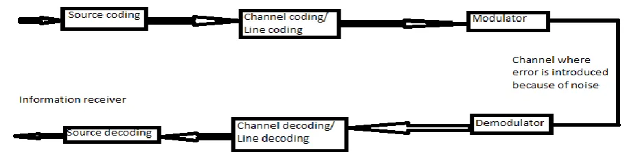
In channel coding, the primary motive for the encoder is to map the incoming digital signal into a channel input and for the decoder to map the channel output into an output signal so that there is minimal effect of noise on the communication channel. It means that the synergetic role of the channel and coding technique is to assure a reliable communication over a noise containing channel. This is done by introducing check bits in a predetermined style in the channel encoder and utilizing it in the decoder to reformulate the original input sent by the encoder as close to reality as possible. Thus in source coding, redundant bits are removed whereas in channel coding, redundancy is introduced in a controlled manner.
1.1 Introduction to VHDL:
VHDL is a programming language that has been designed and optimized for describing behavior of digital communication systems. VHDL has features considerate for describing the behavior of electronic components ranging from simple logic gates to entire processors and custom chips. Features of VHDL allow electrical aspects of circuit behavior such as rise and fall times of signals, delays through gates, and functional operation to be very accurately described. The resulting VHDL simulation models can be used as building blocks in larger circuits using schematics, block diagrams or system-level VHDL descriptions for the purpose of simulation
1.2 Advantages of VHDL:
Figure 1: Block diagram of a digital comm. system
2.
FPGA IMPLEMENTATION
2.1 What is an FPGA?
Field Programmable Gate Arrays (FPGA’s) are programmable chips that can implement almost any digital logic circuit. FPGAs have seen a rapid growth and drastic increase in popularity in recent years due to lower and cheap product development costs and expenditure achieved through design flexibility and extremely negligible overhead. Correspondingly, the need for high-performance CAD tools for FPGAs has never been greater.
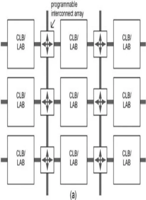
The Computer Aided Design flow for FPGAs commence with an explicit description of the circuit, usually in the form of a hardware description language (HDL) such as VHDL. Once the description is verified through simulation, synthesis is done where the description is synthesized into a gate-level network which are made up of primitive gates. Next, technology mapping is carried out where the gate-level network produced in synthesis is converted into a network of programmable logic blocks (PLBs). After technology mapping, PLBs are grouped together into regular clusters called clustered logic blocks (CLBs). Clustering PLBs into CLBs has proven to be of great importance in order to improve the performance of FPGAs both in terms of area and speed. After clustering, placement and routing are then performed to physically arrange the CLBs on the FPGA and assign routing tracks and switch connections for CLB connections. Figure below shows a generic FPGA architecture in which CLBs are connected by switch blocks and routing wires.
2.2 Necessity
Use of simple parity allows detection of single-bit errors in a received message. Correction of these errors needs more info, since the location of the corrupted bit must be identified if it is to be corrected. (If a corrupted bit can be detected, it can be corrected by simply complementing its value.) Correction is not possible with one parity bit since any bit error in any position produces exactly the same information, i.e., error. If more bits are included in a message, and if those bits can be arranged such that different corrupted bits produce different error results, then corrupted bits could be identified. Digital communication systems, particularly those used in military, need to perform accurately and reliably even in the presence of noise and interference. Among many possible ways to achieve this goal, forward error-correction coding is the most effective and economical.
2.3 General Algorithm
The algorithm written below helps us to determine parity bits for the implementation of Hamming Code for any number of bits:
1 Start numbering from 1,2,3,4,5 ……. etc 2. Then mention bits in binary.
3. All bits placed in power of two are to be parity bits 4. The remaining bit positions are reserved for data that user wishes to send.
5. Every info bit is included in a set of power of 2 bit, which is decided by its binary bit.
1. Parity bit covers lest significant bit
2. Parity bit 2 covers second least significant bit se. 3. Parity bit 4 covers the third least significant bit set. 4. Parity bit 8 covers the fourth least significant bit set:
bits.
Table 1: CAD flow for FPGA Implementation
[image:3.595.52.232.95.511.2].
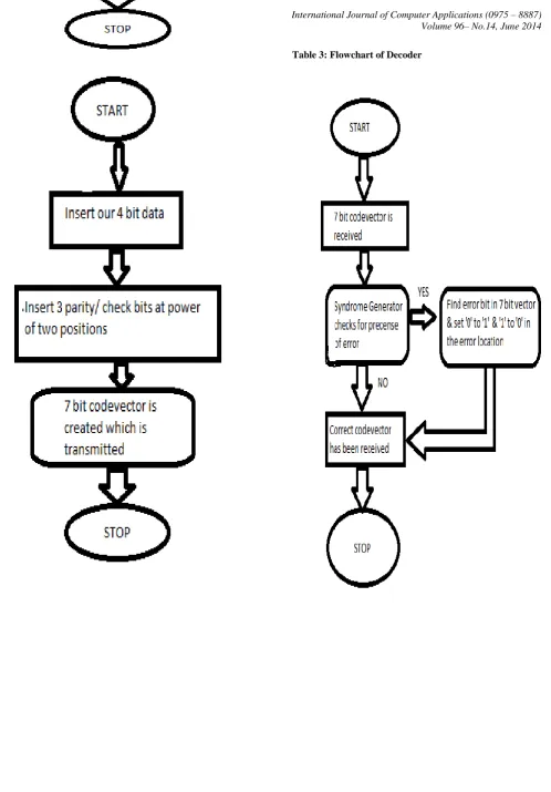
Table 2: Flowchart of Encoder
Flo
[image:4.595.342.543.112.596.2]3.
PERFORMANCE ANALYSIS
Table 5 : Netlists
Parameter Used Total
Core 73 6144(1.19)
IO (W/ Clocks) 22 151(14.57)
Differential IO 0 34(0.00)
GLOBAL(Chip + Quadrant)
1 18(5.56)
PLL 0 1(0.00)
RAM/ FIFO 0 8(0.00)
Low Static ICC 0 1(0.00)
Flash ROM 0 1(0.00)
User JTAG 0 1(0.00)
Table 6: Static Timing Analysis
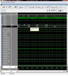
[image:5.595.299.568.96.706.2]Waveforms:
Figure 3: Pre synthesis simulation
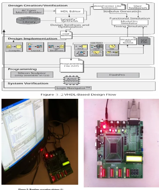
[image:5.595.300.567.108.404.2] [image:5.595.299.572.409.713.2]Actel ProASIC3 Design Flow
Figure 5: Runtime execution picture (1)
Register Transfer Level
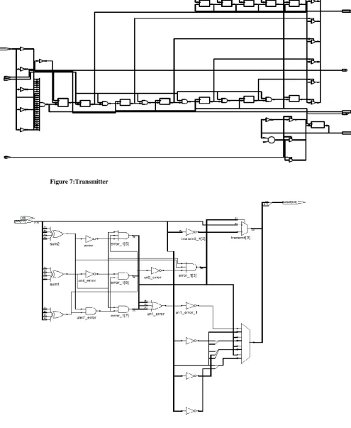
[image:6.595.314.583.407.732.2]Transmitter
Register Transfer Level Views
Figure 7:Transmitter
[image:7.595.55.551.112.716.2]4.
CONCLUSION
This project led to the development of a semiconductor Intellectual Property core that can be implemented for channel encoding. This core uses Hamming Code for error detection and correction. Furthermore, this project aims at using forward error control techniques with minimum redundancy to ensure reliable data transfer, resulting in maximum coding efficiency. Moreover, VHDL design optimization during synthesis has been achieved for obtaining high data rates and throughput, and ability to reconfigure at runtime. The FPGA prototype serves as a predecessor for the development of a fully fledged ASIC.
5.
FUTURE
SCOPE
Use of parallel encoding technique to reduce encoding time
Use of advanced flow control technique
Implementation using hard and soft decoding technique Multi channel support for hard decision decoding
technique
Acknowledgement transfer on data line Asynchronous data transfer mode
Implementing using Viterbi Algorithm and Maximum A Posteriori Algorithm
Clock tree synthesis
Creation of Finite State Automata
Implementation in Simulink so as to get competitive net lists
Implementation for Software Defined Radio
Improving accuracy for industrial applications using Design Rule Checking
Optimizing the throughput using Timing Closure techniques
The project can be scaled up to model and eliminate Additive White Gaussian Noise
Hardware accelerated filter implementation and noise removal
Creation of a Test bench6.
ACKNOWLEDGEMENTS
We express our deepest gratitude towards our sponsor, Mr. S. R. Paspule, Sub Divisional Engineer at Bharat Sanchar Nigam
Limited, Solapur, for providing us with his technical suggestions and for the various exciting scope that our project holds for future implementation in Next Generation Networks and Internet Protocol version 6.
7.
REFERENCES
[1] Datasheet of Actel ProASIC 3 A3P250
[2] Circuit design with VHDL by V. Pedroni
[3] Circuit simulation and design with VHDL by V. Pedroni
[4] VHDL Primer by J. Bhaskar
[5] Digital system design using VHDL by Charles Roth
[6] Fundamentals of Digital Logic Design with VHDL by Brown and Vrasenic
[7] Computer Networks by Tanenbaum 5th Edition
[8] Data Communications and Networking by Behrouz Forouzan
[9] Prof. Rashmi Sinha, Novel Hamming code for error correction and detection of higher data bits using VHDL Intl Jrnl of Scientific & Engg Research, Vol 4, Iss 4, April-2013 272 ISSN 2229-5518
[10]Tongsheng Zhang, Qun Ding, Design of (15, 11) Hamming Code Encoding and Decoding System Based on FPGA,Intl Conf On Instmn, Measmnt Comp, Comm & Contl 2011
[11]Nutan Shep, P.H. Bhagat, Implementation of Hamming code using VLSI,Intl Jrnl of Engg Trnds & Tech Vol4, Iss2–2013
[12]Brajesh Kumar Gupta, Prof. Rashmi Sinha, Various Methodologies used for 25 Bit Information Data String Communication through Hamming Code, Intl Jrnl of Appld Info Systms ISSN: 2249-0868
[13]Leena, Subham Gandhi, Jitender Khurana, Implementation of (7, 4) Hamming Code on CPLD, Intl Jrnl of Engg Research & Tech ISSN: 2278-0181 [14]Varun Jindal, Design of Hamming Code using Verilog