International Research Journal of Engineering and Technology (IRJET)
e-ISSN: 2395 -0056 Volume: 03 Issue: 10 | Oct-2016 www.irjet.net p-ISSN: 2395-0072© 2016, IRJET | Impact Factor value: 4.45 | ISO 9001:2008 Certified Journal
| Page 937
Cascaded Fuzzy Controller based Multilevel STATCOM for
High-Power Applications
Chaparala. Dhanya Sri ¹, Konakala. Prabhakara Rao ²
¹(PG Scholar, Dept of E.E.E (Power Electronics), DVR & Dr. HS MIC College of Technology, A.P, India)
²(Assistant Professor, Dept of E.E.E, DVR & Dr. HS MIC College of Technology, A.P, India)
Abstract
: Voltage unbalance is one of the mainlimitations of cascaded based multilevel STATCOM. In this paper, a simple static var compensating scheme using a cascaded two-level inverter-based multilevel inverter is proposed. The topology consists of two standard two-level inverters connected in cascade through open-end windings of a three-phase transformer. A fuzzy logic control scheme is proposed for the controlling operation of STATCOM. By using the Fuzzy controller in this circuit THD can be reduced. The simulation study is carried out in MATLAB/SIMULINK to predict the performance of the proposed scheme under balanced and unbalanced supply voltage conditions. The presence of Fuzzy controller the disturbances normalized which enhances system performances.
Keywords: Voltage balance, multilevel inverter, power quality (PQ), static compensator (STATCOM), Fuzzy Logic Controller.
1. INTRODUCTION
The utilization of flexible air conditioning transmission frameworks (FACTS) controllers, as an example, static compensator (STATCOM) and static synchronous arrangement compensator (SSSC), is expanding effective frameworks. this is often due to their capability to settle the transmission frameworks and to enhance power quality (PQ) in conveyance frameworks. STATCOM is magnificently acknowledged as adependable receptive force controller replacing ordinary var compensators, as an example, the thyristor-exchanged capacitor (TSC) and the thyristor controlled reactor(TCR).This device provides receptive force pay, dynamic force swaying damping, gleam construction, voltage regulation, so on [1]. By and large, in high-control applications, var pay is accomplished utilizing multilevel inverters [2]. These inverters comprise of an expansive number of dc sources that are usually acknowledged by capacitors. Henceforth, the converters draw a bit measure of dynamic energy to keep up dc voltage of capacitors and to repay the misfortunes within the device. Then again, because of confound in conductivity and exchanging
misfortunes of the exchanging gadgets, the capacitors voltages are lopsided. Adjusting these voltages may be a significant examination challenge in multilevel inverters. The topology consists of standard multilevel/two-level inverters connected in cascade through open-end windings of a three-phase transformer. Such topologies are standard in high-power drives. one among the advantages of this topology is that by maintaining asymmetric voltages at the dc links of the inverters, a number of levels within the output voltage wave form can be increased.
This improves PQ. Therefore, overall control is simple compared to conventional multilevel inverters various var compensation schemes based on this topology are reported during three-level inverter and two level inverter are connected to either aspect of the transformer low-voltage winding. The dc-link voltages are maintained by separate converters. In three-level operation, it is obtained by using standard two-level inverters. In this paper, a static var compensation arrange is proposed for a two-level inverter-based multilevel inverter. The topology utilizes standard two-level inverters to accomplish the multilevel operation. The dc-link voltages of the inverters are managed at every level to obtain four-level operation. To check the adequacy of the proposed control procedure, the modernization study is completed for adjusted and asymmetrical supply-voltage conditions.
This paper is organized as follows: The proposed control scheme is given in Section II. Stability analysis of the converter is discussed in Section III. Simulation and experimental results are conferred in Sections IV and V, respectively.
2. CASCADED TWO-LEVEL INVERTER-BASED
MULTILEVEL STATCOM
International Research Journal of Engineering and Technology (IRJET)
e-ISSN: 2395 -0056 Volume: 03 Issue: 10 | Oct-2016 www.irjet.net p-ISSN: 2395-0072© 2016, IRJET | Impact Factor value: 4.45 | ISO 9001:2008 Certified Journal
| Page 938
voltages of the inverters are maintained constant and modulation indices are controlled to achieve the specified objective. The proposed control scheme is derived from the AC side of the equivalent circuit that is shown in Fig. 3. in the figure, ' ' '
,
,
b ca
v
v
v
are supply voltages observed cardinal side of the transformer,r
a,
r
b,
r
c are the resistances that represent the losses within the transformer and two inverters,L
a,
L
b,
L
care discharged inductances of transformer windings,e
a1,
e
b1,
e
c1 and2 2 2
,
b,
ca
e
e
e
are the output voltages of inverters 1 and 2, respectively.r
1,
r
2 are the discharge resistances of dc link capacitorsC
1C
2 respectively. Assumingr
a
r
b
r
c
r
,
,
L
L
L
L
a
b
c
and applying KVL on the AC side, the dynamic model can be derived using as dt di dt di dt di c b a ' ' ' = L r L r L r 0 0 0 0 0 0 ' ' ' c b a i i i +
L
1
) ( ) ( ) ( 2 1 2 1 2 1 ' ' ' c c b b a a c b a e e e e e e v v v (1)This equation represents the mathematical model of multilevel STATCOM in the stationary coordinate system. The control block for STATCOM is shown in the figure below. The control for STATCOM is achieved by using the unit signals sin and cost which are generated from phases fast loop that is provided by three phase supply voltages. using these unit signals the mathematical model represented in equation(1) is transformed into the synchronously rotating reference system .Therefore the d-q axes
reference voltage components of the converter are controlled as, ' ' 2 * ' ' 1 * q d q d q d
v
Li
x
e
v
Li
x
e
(2) (3) Where 'd
v
is the d-axis voltage component of the AC source and ' ',
qd
i
i
are d-q axes current components of the cascaded inverter, respectively. The synchronouslyrotating frame is aligned with source voltage '
q
v
vector so that the q-component of the source voltage is made zero. The control parameters and are controlled as follows:
)
)(
(
)
)(
(
' * 2 2 2 ' * 1 1 1 q q i p d d i pi
i
s
k
k
x
i
i
s
k
k
x
(4) (5)The d-axis reference current
i
*d is obtained as
(
)
(
)
)
(
3 3 *1 *2 1 2* dc dc dc dc i p
d
V
V
V
V
s
k
k
i
(6)
International Research Journal of Engineering and Technology (IRJET)
e-ISSN: 2395 -0056 Volume: 03 Issue: 10 | Oct-2016 www.irjet.net p-ISSN: 2395-0072© 2016, IRJET | Impact Factor value: 4.45 | ISO 9001:2008 Certified Journal
| Page 939
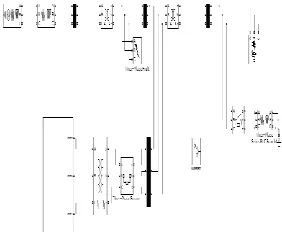
Fig- 2: Cascaded two-level inverter-based multilevel STATCOM.
Fig-3:
Equivalent circuit of the cascaded two-level inverter based multilevel STATCOM
3. PROPOSED CONTROL STRATEGY
The control block diagram is shown in Figure4.The unit signals Cos and sin are generated from the phase-locked loop (PLL) using three-phase supply voltages [14]. The converter currents are transformed to the synchronous rotating system using the unit signals. The switching frequency ripple within the converter current loops, *
q
i
the controller generates d-q axes reference voltages, *
d
e
and *q
e
for the cascaded inverter. With these reference voltages, the inverter provides the required reactive current draws required active current to regulate total dc-link voltage. However, this will not ensure that individual dc-link voltage is controlled at their respective reference values. Hence additional control is required control individual dc-link voltages of the inverters.
Fig-4: Proposed system controlled proposed strategy
3.1
DC-Link Balance Controller
The resulting voltage of the cascaded device is given as,
2 2
q d
I
e
e
e
The active power transfer between the supply and electrical converter depends on and is usually small within the inverters supplying var to the grid [1]. Hence, may be assumed to be proportional to equivalent weight. Therefore, the -axis reference voltage component of inverter-2 eq2*is derived from controlling the dc-link voltage of inverter-2 as,
)
)(
(
4 4 *2 2*
2 dc dc
i p
q
V
V
s
k
k
e
(7)
The q-axis reference voltage component of inverter-1 * 1
q
e
is obtained as* 2 * *
1 q q
q
e
e
e
(8)The power transfer in inverter-2 is directly controlled, whereas for the inverter-1, and it's controlled indirectly. Therefore, throughout the disturbances, the dc-link voltage of inverter-2 is improved to its reference quickly compared to the inverter-1. Using *
1
d
e
ande
*q1,
the reference voltages are generated in stationary reference system for inverter-1 and using *2
d
e
and * 2q
e
for inverter-2. The reference voltages generated for inverter-2 are in phase opposition to that of inverter-1. From the reference voltages, gate signals are generated using the sinusoidal pulse-width modulation (PWM) technique [15]. Since the two inverters' reference voltages are in phase opposition, the predominant harmonic appears at double the switching frequency.3.2 Fuzzy Logic Controller
International Research Journal of Engineering and Technology (IRJET)
e-ISSN: 2395 -0056 Volume: 03 Issue: 10 | Oct-2016 www.irjet.net p-ISSN: 2395-0072© 2016, IRJET | Impact Factor value: 4.45 | ISO 9001:2008 Certified Journal
| Page 940
applications. The fuzzy inference may be a technique that interprets the values in the input vector and, based on user-defined rules, assigns values to the output vector. using the interface editors and viewers within the fuzzy logic toolbox, you'll build the principles set, define the membership functions, and analyze the behavior of a fuzzy inference system (FIS). The subsequent editors and viewers are provided.
Fig-5:
Fuzzy inference system
This system consists of four main parts. First, by using the input membership functions, inputs are Fuzzified then based on rule bases and the interfacing system, outputs are produced and finally, the fuzzy outputs are Defuzzified and they are applied to the main control system. The error of inputs from their references and error deviations in any time interval are chosen as MATLAB. The output of the fuzzy controller is the value that should be added to the prior output to produce new reference output as shown in Figs.6 to 9.
Fig-6:
Selection of input and output variables.
Fig-7: Input1 membership function
Fig-8: Input2 membership function.
International Research Journal of Engineering and Technology
(IRJET)
e-ISSN: 2395 -0056 Volume: 03 Issue: 10 | Oct-2016 www.irjet.net p-ISSN: 2395-0072© 2016, IRJET | Impact Factor value: 4.45 | ISO 9001:2008 Certified Journal
| Page 941
4. SIMULATION RESULTS AND
DISCUSSION
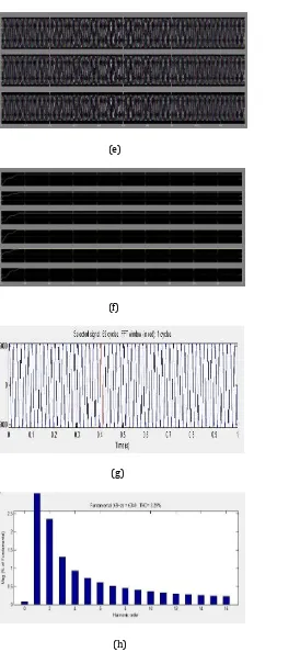
[image:5.612.226.562.81.673.2]The simulation study is carried out using MATLAB/SIMULINK. System parameters are given in Table 1. The system configuration is shown in fig10
Fig-10: Simulation circuit diagram of a Proposed STATCOM fuzzy logic controller
TABLE 1
SIMULATION SYSTEM PARAMETERS
(a)
(b)
(c)
(d)
Results of Proportional and integral controller
Rated Power 5 MVA
Transformer voltage rating 11KV/400
AC supply frequency, ƒ 50 Hz Inverter-1 dc link voltage,
1
dc V
659V Inverter-2 dc link voltage,
2
dc V
241V Transformer leakage
reactance, X1 15%
Transformer resistance, R 3% DC link capacitances, C1,C2 50mF
[image:5.612.39.180.194.310.2]International Research Journal of Engineering and Technology (IRJET)
e-ISSN: 2395 -0056 Volume: 03 Issue: 10 | Oct-2016 www.irjet.net p-ISSN: 2395-0072© 2016, IRJET | Impact Factor value: 4.45 | ISO 9001:2008 Certified Journal
| Page 942
(e)
(f)
(g)
(h)
Results of fuzzy logic controller
DISCUSSION
Here the above figures (a) to (d) are the results of PI controller. Where in figure (a) the execution time taken in 0 to 1 are the fault. Before 0 to 1 it is prefault. After 0 to 1 it is post fault. Actually we create line fault, initially there is no fault. By using PI controller time gap after 0 to 1 STATCOM automatically ON and clears the fault. Coming to figure (b)
dc
[image:6.612.43.317.84.678.2]V
values are represented. Instantaneously it increases and decreases and equivalently ON and OFF. In figure we representsV
dc,V
abc.
Figures (c) and (d) represents FFT Analysis and Total HarmonicDistortion(THD).In PI controller THD value we got is 9.94% that showed in above figure.
Figures (e) to (h) are the results of Fuzzy Logic controller. Coming to fuzzy it is easy to write our own rules and also own membership functions. Fuzzy controller can instantaneously ON and OFF. So it is easy when compared with PI controller. Where in PI controller we occurs some faults. So in fuzzy it overcomes that faults and reduces fault and output comes smooth compares with PI. In fuzzy the THD value is 3.29% that shows in above figure.
Comparetively when compared with PI Fuzzy logic can overcome errors and decreases THD value.
5. CONCLUSION
A simple STATCOM theme using a cascaded two-level inverter-based multilevel inverter is presented in this paper. The proposed topologies have two VSI based two level inverters are connected in cascade through open-end windings of a three-phase transformer and filter parts. Converter fed dc-link voltages is regulated at different levels to obtain four-level operation. The proposed STATCOM structure inverter has operated below MATLAB/SIMULINK settings and also the results are verified in balanced and unbalanced conditions. Further, stability behavior of the topology is investigated. The dynamic model is developed and transfer functions are derived. The system behavior is analyzed for various operating conditions.
6. REFERENCES
International Research Journal of Engineering and Technology (IRJET)
e-ISSN: 2395 -0056 Volume: 03 Issue: 10 | Oct-2016 www.irjet.net p-ISSN: 2395-0072© 2016, IRJET | Impact Factor value: 4.45 | ISO 9001:2008 Certified Journal
| Page 943
[3] H. Akagi, S. Inoue, and T. Yoshii, “Control and performanceof a transformerless cascaded PWM STATCOM with starconfiguration,” IEEE Trans. Ind. Appl., vol. 43, no. 4, pp. 1041–1049, Jul./Aug. 2007.
[4] Y. Liu, A. Q. Huang, W. Song, S. Bhattacharya, and G. Tan,“Smallsignal model-based control strategy for balancingindividual dc capacitor voltages in cascade multilevel inverterbasedSTATCOM,” IEEE Trans. Ind. Electron., vol. 56, no. 6, pp.
2259–2269, Jun. 2009.
[5] H. P.Mohammadi andM.T. Bina, “A transformer less mediumvoltageSTATCOM topology based on extended modularmultilevel converters,” IEEE Trans. Power Electron., vol. 26, no.5, pp. 1534–1545, May 2011.
[6] X. Kou, K. A. Corzine, and M. W. Wielebski, “Overdistentionoperation of cascaded multilevel inverters,” IEEE Trans. Ind.Appl., vol. 42, no. 3, pp. 817– 824, May/Jun. 2006.
[7] K. K. Mohaptra, K. Gopakumar, and V. T. Somasekhar, “A harmonic elimination and suppression scheme for an open-end winding induction motor drive,” IEEE Trans. Ind. Electron., vol.50, no. 6, pp. 1187–1198, Dec. 2003.
[8] Y. Kawabata, N. Yahata,M. Horii, E. Egiogu, and T.Kawabata, “SVG using open winding transformer and twoinverters,” in Proc., 35th Annual IEEE Power Electron.Specialists Conf., 2004, pp. 3039–3044.
[9] S. Ponnaluri, J. K. Steinke, P. Steimer, S. Reichert, and B.Buchmann, “Design comparison and control of medum voltageSTATCOM with novel twin converter topology,” in
Proc., 35thAnnu. IEEE Power Electron. Specialists Conf., 2004, pp. 2546–2550.
[10] N. N. V. Surendra Babu, D. Apparao, and B. G. Fernandes,“Asymmetrical dc link voltage balance of a cascaded two levelinverter based STATCOM,” in Proc., IEEE TENCON, 2010, pp.483–488.
[11] IEEE Criteria for Class IE Electric Systems, IEEE Standard141-1993.
[12] C. Schauder and H. Mehta, “Vector analysis and control ofadvanced static VAr compensators,” in Proc. Inst. Elect. Eng. C.,Jul. 1993, vol. 140, no. 4, pp. 299–305.
[13] D. G. Holmes and T. A. Lipo, “IEEE series on powerengineering,” in Pulse Width Modulation for Power Converters:
[14] K. R. Padiyar and A. M. Kulkarni, “Design of reactive current and voltage controller of static condenser,” Elect. Power Energy Syst., vol. 19, no. 6, pp. 397–410, 1997. [15] A. Leon, J.M.Mauricio, J. A. Solsona, and A. Gomez-Exposito, “Software sensor-based STATCOM control under unbalanced conditions,” IEEE Trans. Power Del., vol. 24, no. 3, pp. 1623–1632, Jul. 2009.
CHAPARALA. DHANYA SRI received B.Tech degree in Electrical & Electronics Engineering, from Dhanekula Institute of Engineering and Technology in 2014, Gangur, Vijayawada and pursuing M.Tech in Power Electronics, at DVR & Dr. HS MIC College of
Technology,Kanchikacherla. Area of
interest includes research in Power Electronics.