POWER OPTIMIZED CLOCK GATED ALU FOR LOW
POWER PROCESSOR DESIGN
1L.RAJA, 2Dr.K.THANUSHKODI
1
Prof., Department of Electronics and Communication Engineeering , Angel College of Engineering and Technology, Tirupur,India
2
Director.,Akshaya College of Engineering and Technology, Coimbatore,India
E-mail: [email protected] , [email protected]
ABSTRACT
Arithmetic and Logic Unit (ALU) is one of the frequent and the most fundamental component in low power processor design. Besides Power consumption due to clock gated ALU can be significant in high performance systems. In general the functionality of ALU is a mixture of arithmetic and logic operations which are realized by means of combinational circuits. In this research work the power flow analysis of clock gated ALU circuits is analyzed and optimization of clock gated ALU power supply unit is done through special handing technique. The proposed design which controls the power supply unit of ALU via Clock Gated Double Edge Triggered (CGDET)flip-flop technique which outperforms the traditional Clock Gated Single-Edge-Triggered (CGSET) flip-flop and it reduces the power consumption by 2.2% while keeping the same data rate. In contrast with existing techniques the proposed method has simpler structure, lower delay time, condensed Power Delay Product (PDP), Energy Delay Product (EDP) and Static current has been tabulated. The work suggests that clock gated double edge triggering provides optimized power management for ALU design.
Keywords: Clock Gated SingleEdgeTriggered (CGSET) FlipFlop, Clock Gated Double Edge
-Triggered (CGDET) Flip-Flop, Power Delay Product, Energy Delay Product, Arithmetic And Logic Unit
I. INTRODUCTION
Now a day’s power management (power density in W/mm2) is the mounting issue in all part of chip design. As a chip manufacture, at architecture stage (all designs of 90nm and below) low power techniques need to be employed from RTL to GDSII. Due to aggressive leakage currents indeed cause high power (I2R) loss in CMOS circuitry. In related to the design issues some of the equations as follows
=∑ (1)
Dynamic power consumed by the device, when it switches from one state to another state. Dynamic power consists of switching power, consumed while charging and discharging the loads on a device, and internal power (also referred to as
Short circuit power), consumed internal to the device while it is changing state.
= + (2)
= ∑ (3)
= ½ × CL × V2 × TR (4)
conventional CG (clock gated) circuits IV. Special handling techniques V.Results and comparison VI. Conclusion and future work as follows.
1.1 Statement of the Problem
Issues due to Dynamic power dissipation has analyzed and reduced using different traditional The techniques such as 1) Latch-free based CG design 2)Latch-based CG design 3)Flip-flop based CG design 4)Single edge CG design. Power dissipation Issues suffered by the traditional approach is overcome by the proposed method.
2. RELATED WORKS
There are various techniques available to optimize power in VLSI circuits.
Some of them are:
1. Clock tree optimization and clock gating 2. Operand isolation
3. Logic restructuring 4. Logic resizing
5. Transition rate buffering 6. Multi-Vth:
7. Multi-supply voltage 8. Dynamic voltage scaling
9. Adaptive voltage and frequency scaling 10. Memory splitting
Clock signals are in toggle mode even there is no input, these signals dissipate dynamic power. By means of gating clock, 1.No loss during idle state the processor turns off 2. Power saved due to clocking gates 3. Logic on enable circuit is removed when it is in ideal state and return to function only when the inputs are enabled [5]. Recently researchers started concentrating on RTL design due to clock gating. The conditional logic block in the original RTL, before and after the clock-gating attribute is set [2]-[3].If the clock-gating logic of different registers in the design uses the same enable signal, RTL Compiler can merge these clock-gating instances for any such identically gated registers. This process is called clock-gating de-cloning. Clock gating utilize less power while comparing concerning with clock enable mode [1].In [6] pipelined architecture with low powered efficient ALU arrangement was developed. ALU with 16 functions, dedicated module for each function is established [7] particular module will perform operation to obtain to reduce power.
3. CG CIRCUITS-CONVENTIONAL APPROACHES
3.1. Latch Based and Latch Free Based Clock Gating Design
The latch based design also allows a very natural and safe clock gating methodology [4], as shown in the Figure.2.it shows a simple and safe way of generating enable signals for clock gating. This method gives glitch free clock signals without adding of memory elements, as it is needed with D-flip-flop clock gating. it performs nicely the time borrowing and seems to analyze correctly the clocks for speed optimization .to ensure a glitch free clock, this AND gate has to be placed as shown in the Figure.1.thsi can be easily done manually by placing these AND gates in a separate level of hierarchy. With latch based design, the clock skew problem becomes relevant only when it value is close to the non-overlapping of the clock. It in turn increase the power consumption of the circuit than latch free based design because Using simple gates, latch free circuits can be designed as shown in Figure.2. In this circuit the operation of EN signal should be set 1 for all active edges to avoid truncate. If enable signal terms to be zero in between the clock pulse will make the gated clock ended before his life time This constraint makes the latch-free clock gating style inappropriate than latch based design.
ALU CLK GATE
From Data Reg(A) Carry_In
From Op Reg(B)
Sel[3:0] EN
CLK LATCH
Figure 1: Latched clock gating based ALU
Figure 2: Latch free clock gating circuit
3.2. Single Edged Flip Flop Based Clock Gated Design
the clock pulse, when the input data is clocked. Clock triggering occurs at a voltage level and is not directly related to the rise time of the clock pulse [5]-[6]. Function of clock has represented in the equation (1).
, , (5)
The Flip-Flop (FF) based clock gate as shown in the Figure.4 Consists of a level sensitive latch in design to hold the enable signal from the active edge to the inactive edge of the clock as shown in Figure.5. As it is triggered at one edge it has high over head than proposed dual edge method.
ALU CLK GATE
From Data Reg(A) Carry_In
From Op Reg(B)
Sel[3:0] EN
[image:3.595.293.513.73.392.2]CLK FF
Figure 3: FF Clock Gated Based ALU
Figure 4: Clock Gated Single Edged Triggered Method
4. SPECIAL HANDLING TECHNIQUES
4.1. Dual Edge Triggering Clock Gated Design
Double edge triggered (DET) flip flop is triggered on both edges of the clock pulses instead of only one edge. Using DET flip flop the clock frequency can be halved for the same data rate, thus reducing the power dissipation on the clock
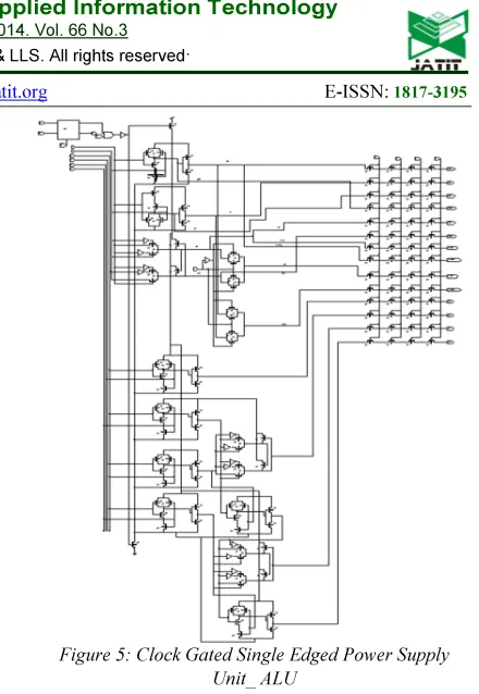
Figure 5: Clock Gated Single Edged Power Supply Unit_ ALU
[image:3.595.79.519.80.505.2]Distributing network. The DET and SET flip flops, static and dynamic, as shown in the Figure.6.both SET and DET flip flops have two D-type latches. In the DET flip flop the latched are arranged in parallel while in the SET flip flop they placed serially.DET flip flop have been shown to have lower energy requirement (20%) then SET flip flops, with only a limited overhead in complexity. This has confirmed by analytical and simulation means. Function of clock has represented in the equation (2).
, , (6)
[image:3.595.99.290.420.558.2]Figure 6: Clock gated Double Edged triggered method
[image:4.595.98.274.341.533.2]
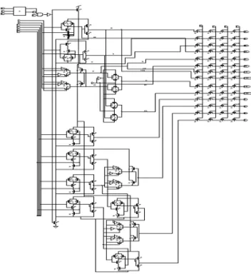
Figure 7: Clock gated Double Edged power supply unit_ ALU
5. RESULTS AND COMPARISON
5.1. Power
Power dissipated to drive the input of the flip
flop is due to switching power, short-circuit and leakage power. [11].
Power= + + (7)
Switching Activity Factor: α
If the signal is a clock, α = 1 then If the signal switches once per cycle, α = ½.besides For Dynamic gates: switch is either 0 or 2 times per cycle, α = ½ and for the Static gates: depending on design, but typically α = 0.1
= a .f.Ceff .Vdd2 (8)
Short-circuit power occurred when there is a transition between VDD and GND occurs
= Isc .Vdd.f (9)
= f (Vdd, Vth, W/L) (10)
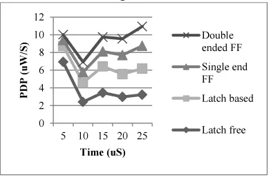
The power comparison for various styles due to switching activity has shown in Table.1.
Table 1: Shows the Power of various styles
Time(u S)
Power(W)
Latch free
Latch based
Single end FF
Double ended FF
5 1.386 0.358 0.135 0.123
10 0.241 0.218 0.118 0.115
15 0.230 0.198 0.113 0.108
20 0.149 0.129 0.107 0.0924
25 0.129 0.118 0.103 0.0873
[image:4.595.309.503.434.559.2]Besides the comparison of various styles with respect to power Vs time has shown in the Figure.8
Figure 8: Power graph comparison for various styles
5.2. Power Delay Product
For most of the clock and data patterns the
proposed method has the finest power-delay product among the various CG methods. [11]-[12].In particular data changes with respect to clock edge, the modified proposed method is the most attractive choice. For example, when clock activity rate is 0.5 and data activity for single end FF is same as input for the positive edge of the clock and unequal at the negative edge. In case of double end FF the data activity is same as input data for both the edges. The power comparison for
0 0.5 1 1.5 2 2.5
5 10 15 20 25
P
o
w
e
r
(W
)
Time (uS)
various styles due to switching activity has shown in Table.2.
Table 2: Shows the PDP of various styles
[image:5.595.81.267.181.326.2]Change of the PDP (p*t) for the conventional and proposed method with respect to switching time is has shown below in Figure.9
Figure 9: Power delay product graph comparison for various styles
5.3. Energy Delay Product
The three foremost sources of energy utilization in a flipflop is input energy, which represents the energy dissipated to drive the input of the flipflop, clock energy, the energy dissipated at the internal nodes, internal energy the energy dissipated in the local clock buffer driving the clock. The most significant actuality about the energy dissipation of a flipflop is the function of input activity, besides also a function of clock activity. Energy can be saved by gating the clock, as is commonly done in proposed low-power designs. Table.3.shows the EDP (p*t2) of various styles. Then the corresponding variation in the static current has shown which indicates the double edge triggered
structure has less static current than the remaining methods.
Table 3: Shows the EDP of various styles
6. CONCLUSION
Power reduction deals with synthesis, design at circuit level and placement and routing stages, now moved to the System Level and Register Transfer Level. The inactive unit of the ALU design is switch off by clock gating method and it helps to reduce overall power consumption in the system. In low power processor design the power flow analysis of the circuits has been studied and tabulated (T.1 & T.2).From the analysis it is noticed that the clock gated double edge triggering consumes less power when compared to conventional clocked gated single edge triggered flip flop. Further the analysis has been extended to latch free, clock gated latch with single edge and double edge circuits for ALU design, it is noticed that clock gated double edged circuit consumes low power. Hence the ALU unit designed with clock gated double edge circuit performs efficiently in terms of PDP (p*t), EDP
(p *t2) and static current. This paper indicates that if the SET flip-flops are linked in series then the conventional structure can be plainly replaced by DET flip-flops linked in parallel.
In order to reduce dynamic power, Clock gating technique is one of the preferable methods. Reduction of leakage power consumption is done through extended clock gating technique. When clock gating circuit used in power supply unit of clock gated ALU which produces power noise it in turn reduced by making use of active resistance method in power supply unit for future enhancement.
0 2 4 6 8 10 12
5 10 15 20 25
P
DP
(
u
W
/S
)
Time (uS)
Double ended FF Single end FF Latch based
Latch free
Time(us) PDP(uw/s)
Latch free
Latch based
Single end FF
Double ended FF
5 6.93 1.79 0.675 0.615
10 2.41 2.18 1.18 1.15
15 3.45 2.97 1.695 1.62
20 2.98 2.58 2.14 1.848
25 3.225 2.95 2.575 2.182
Circuits EDP
(Energy Delay Product)
W/S
Static current
I(mA)
Latch Free 147.68e-017 5.1311
Latch Based 106.71e-017 2.929
FF With Single Edge 55.37e-016 2.5163
[image:5.595.89.285.385.515.2]List of Nomenclature
CL: Capacitive loading, V: Voltage level, TR: Toggle rate, a = switching activity, f = switching frequency, Ceff = effective capacitance, Vdd = supply voltage, Isc = short-circuit current during switching, Vdd = supply voltage, f = switching frequency, Vdd = supply voltage, Vth = threshold voltage, W = transistor width, L = transistor length.
REFERENCES
[1] J.P.Oliver, J. Curto, D. Bouvier, M. Ramos, and E. Boemo, “Clock gating and clock enable for FPGA power reduction”, in Proc. 8th Southern Conference on Programmable Logic (SPL), pp. 1-5, 2012.
[2] Jagrit Kathuria, M.Ayoubkhan & Arti Noor Centre for Development of J. Shinde and S. S. Salankar, “Clock gating-A power optimizing technique for VLSI circuits”, in Proc. Annual IEEE India Conference (INDICON), pp. 1-4. [3] Advanced Computing, NOIDA, India. Review
of Clock gating technique MIT International journal of Electronics and Communication Engineering, Vol.1 No.2 Aug 2011 pp106-114 ISSN 2230-7672 @ MIT Publication.
[4] J. Castro, P. Parra and A. J. Acosta, “Optimization of clock-gating structures for low-leakage high-performance applications” in Proceedings of IEEE International Symposium on Efficient Embedded Computing, pp. 3220-3223, 2010.
[5] V. Khorasani, B. V. Vahdat, and M. Mortazavi, “Design and implementation of floating point ALU on a FPGA processor,” IEEE International Conference on Computing, Electronics and Electrical Technologies (ICCEET), pp. 772-776, 2012.
[6] S.Cisneros, J. J. Panduro, J. Muro, and E. Boemo, “Rapid prototyping of a self-timed ALU with FPGAs,” in Proc. International Conference on Reconfigurable Computing and FPGAs, pp. 26-33, 2012.
[7] B.S. Ryu, J. S. Yi, K. Y. Lee, and T. W. Cho, “A design of low power 16-bit ALU,” in Proceedings of the IEEE TENCON Conference, pp.868-871, 1999.
[8] M.Afghahi and J. Yuan, “Double edge-triggered D-flip-flops for high-speed circuits,” IEEE J. Solid-State Circuits, vol.26, no.8, pp.1168-1170, Aug. 1991.
[9] A.Gago, R. Escano and J. A. Hidalgo, “Reduced implementation of D-type DET flip-flops”, IEEE J. Solid-State Circuits, vol.28, no.3, pp.400-402, Mar. 1993.
[10] A R.Hossain, L. D. Wronski and A. Albicki, “Low Power Design using Edge Triggered Flip-flops”, IEEE Trans. Systems VLSI S. Solid-State Circuits, Vol.2, no.2, pp.261-265, June 1994.
[11] N.H.E.Weste and K. Eshraghian, “Principles of CMOS VLSI Design”, A System Perspective Reading MA: Addison-Wesley),
1993.