Semiconductor Technologies
Digital Technical Journal
Digital Equipment Corporation
CrJIIer Des(� II
'f/w (..\10 .•. j f!I'IICI'SSCS d!'SCI'ifJ!'d ill Ibis [.,·:me (//'l' 1/S!'d to flllifd fJigitol :\ I.Jig/.J-jJ('J1i Jl'llltt!JCe ,\'1:1.\ wuf A/jJ/)(1 .! f()(ri ('/.JifJS. 'I he fJhofrmlicrop,rafJ/J IIIII JIII' COI'l'l'jtJCI/ses 011 1/.w b��b-sfJeed clue/..• ifl'il'e/' {[ 11!1 /IIIII '('/'
jmds
u{
1/.Je ..1/jJ/Ill
.! /()()-i 1/JiCI'IIjii'IICI'SSfJ/; II •/I feboj)('l'llles fll (/duck mfc•
uf.!OO
.till::.7be JI!IIJ/Imlicm.r<.ruf'l�l' is f�J' Peter (.{lfillel!u c111d Uria11 f:'duwds
I'�' !Jigi
tat:� \('ill iCII//(//1('/(1/' rllllfl)'.�is La fir IJ'((/IJI:J'. 1/udSflll, .II. I.I he u ;I ·er design i.\ f�J' II ike (ill I u
{
!Ju
a
111 ic (,t JIII/II wiical it ills. Inc.Editorial
.J:ttll' C. BlakL·. Ediwr
Helen 1.. Patn:r,on .. \S>ociate Editor K:nhleen M. Stetson. ,\s">eiatt· Editor Circulation
C:lllll'rinc .VI. l'hillips, Administrator Shen·y L. Gonzalez
P.-oduction
Mildred R. Rosenzweig, Production Editor Margaret 1.. Burdine. 'J)'pographer Pt:ter R. Woodbury. Illustrator Advisory Board
Samuel H. fuller, Chairman Hichard \V Beane
Robert M. Glorioso Richard]. Hull ingsworth Ai:ln G. "'emeth Victor A. V1·ssotsky Gam B. Winters
The /Jigilaf Ti!clllliatfjullmal i' published quartnll' 111' Digital Equipment Corporation. J-i6 :\-lain St reel .\·ll.ll l-.VBI>H. �laynard . .\l:l"achu"·tt' fll7'i i-2'>�1. �ub,cription' to thc.fu/1/'llltl arcS iO.OO l<>r lin1r i"u" and must he prepaid in {I.S. funds. lnilersit\· and college prufc"or' and l'll.D. students in th<: electrical engineering and computer scic.:nce tields n.:-cci,·t: complillll'lltary suh:o-.LTiption:-, upon request. Orders. inquiries. ami addrc" cltang" should he sent to tltc Oigilal h·cblticalfoltl'l[{t{ :It the puhlishnl-lw add res,_ Inquiries can also be sent ekctronic:llly toiJ'Ijlu:<:t!I..I>H:.Co.\1. Single eopic,; and back issues are :ll·ailahk "'" $1h.OO each from Digital Press of Digital Equipment Corporation, I 1\urlington Woocb Dri\'c, Burlington, \L\ OlH:\O-·i�lJ7.
Digital L'mployL'l'S nw\· send suhscription ordtTs on the L''Wi' to IU>VAX::.JOIIRNAI.or hy interoflin· m:til to maibtop \II.< ll·:l/ll(>H.
Orders should include badge JlltmhLT. site· locnioneodc. ami
addr"s. !\II elllploy<TS must ad1·i,e of ch:tnge> of address. Co!l!lllcnr.., on rhe content of an� paper arc \\'t:konH.:d and may he Sl'nt to tiH: editor at the pub! i'hcd-h) or net work addr ·ss. <:opnight ''
1')')2
Digital Equipment Corporation. Copying \Yithout l'cc i� permitted pro\·idvd th;ll ... uch copi...:s :ItT made f(n· usc in cducttinn;.d inslitutinn� h�· Ltcult� JllC!lllwr_.., and an: notdi,u·ihutcd ti1rcommnci:tl aLh'ant:tgc. Ahstr:Kting 1\ith credit of tligital EquipmC'nt Corpor:Jtion·, :�uthoJ·.,Jtip is permitted . . \II riglll' rc"n·ecl.
l'ltc· inl(>rmation in thc.Jutrrllrtl i' 'uhjeu to dJ:utgc without notice :1nd !'<ll!ould nor ht· nHI,trucd :L' .t conllnitnu:nt h�·J>igit;tl Equipment Corpor:tl ion. Digil:tl l-:quipn1l'llt < .orp()r:tt it 111 ;t�;-.unJc ....
no n.· ... ron:-,ihilit � for ;u1y ern'�"' tll.ll nl.t\ appc:tr in tlu .. ·.frJ/11"1/0/. I�S. OX'JH-')01"
Document:Jlioll �umhcr EY-1.'>21 i'.-1>1'
The liJI IIm ing arc t r:llklll:trhs o/ l>i)\it:tl t:quipmcllt. ( :orporati<llt· Ut:C.. I >igit:tl. the· Digital logo. \'AX.\:\" (>0(1!1. \'A"c!U,tlT, \>\ \ t'OR m \ . and\ \IS.
Ill'<. ,\VS i' at r:J<kll'l:trh. ot' �l:ll'dcnl < :ontput<'l' �) 'lL'll". \Ill'!'> i' :t tr:Jdcnt:Jrh. of \til'S Computcr S) '1<'111,, lnc
I' I�< .I·'-:�ntl I I'!U:\I.i arc tr:�Jcm:trh.' oft It · llo:�rd of l'ruo,tn·, • >I l.d:111d Stantord .Juni< >r I ni\ er,it 1.
I
Contents
10 Foreword
R. ]. Hollingsworth
12
Microprocessor Performance andProcess Complexity in CMOS Technologies Bjorn Zetterlund, james A. Farrell, and Thomas
F
Fox25
Numerical Device and Process Simulation Toolsin Transistor Design
Marden H. Seavey, john V faricelli, Nadim A. Khalil, Gerd Nanz, Llanda M. Richardson, Christian
0.
Schiebl, Hamid R. Soleimani, and Martin Thurner39
CMOS-4 Technology for Fast Logic and Dense On-chip MemoryAndre
I. Nasr, Gregory).
Grula, AntonioC.
Berti, and Richard D. jones51
CMOS-4 Back-end Process Development for aSemiconductor Technologies
VLSI
0. 75 pm
Triple-level Interconnection Technology Marion M. Garver, joseph M. Bulger, Thomas E. Clark, jamshed H. Dubash, Lorain M. Ross, and Daniel). Welch73
Implementation of Defect Reduction Strategies into VLSI ManufacturingMary Beth Nasr and Ellen].
Mager
83
A Yield Enhancement Methodology for Custom VLSI MartufacturingRandall S. Collica,
X.
joseph Dietrich, Rudolf Lambracht Jr. , and DavidG.
Lau100 Transistor Hot Carrier Reliability Assurance
in CMOS Technologies
Daniel
B.
jackson, David A. Bell, Brian S. Doyle, Bruce). Fishbein, and David B. Krakauer114
E/ectromigration Reliability of VLS/lnterconnectI
Editor's Introduction
Jane C. Blake Editor
The design of semiconductor chips has been the topic of several past Digital Technical journal issues. With the introduction of Alpha 21064, the world's fastest microprocessor, this issue focuses for the first time on the development of semi conductor technologies that make possible the high performance of D igital's VLSI chips. Engineers in Advanced Semiconductor Development present in-depth views into CMOS-4 technologies, which pro duce microprocessors with up to 1.7 million transis tors and operating frequencies as high as 200 MHZ.
The significant increase in p erformance achieved
with each generation of CMOS technology is in part
the resul t of a synergistic relationship between microprocessor design and process engineers. In their paper on process technology contributions to microprocessor performance, Bjorn Zetterlund, Jim Farrell, and Frank Fox describe the scaling the
ory that has led to a doubling of gate density and an increase of 30 percent in gate speed in fou r suc
cessive CMOS generations. They discuss process
features implemented in CMOS-4, and close with a dis
cussion of models that predict process variations. Models and tools, essential in providing design ers early insight into the characteristics of the tran sistors to be fabricated, are the focus of a paper by Marden Seavey, john Faricell i , Nadim Khalil, Gerd Nanz, Llanda Richardson, Christian Schiebl, Hamid Soleimani, and Martin Thurner. The authors describe several physical models that accurately simulate transistor behavior, and present numerical mathe matical methods used to enhance existing simula tors. An overview of Digital's and others' efforts to integrate simulation tools concludes the paper.
The need for both high-density logic gates and on-chip cache memory in m icroprocessors pre sents special challenges to process engineers. Andre Nasr, Greg Grula, Antonio Berti, and Rich
2
jones review the front-end process (formation of device and local interconnect) for the CMOS-4
0.75-/Lm technology and the steps taken to meet design requirements. They also describe the effects on submicron devices related to the scaling of fea ture sizes and examine some solutions.
Goals for the back-end process (formation of global metal interconnect) were also driven by the logic design requirements for higher circuit density. In addition, back-end development goals included the continued use of equipment developed for the 1 .0-�Lm CMOS-3 technology. Marion Garver, joe Bulger, Tom Clark, Jamshed Dubash, Lorain Ross, and Dan Welch relate how tools were modified for CMOS-4 and describe new blanket tungsten and pla narization processes for submicron devices.
To produce a specified yield of CMOS devices, defect reduction and yield enhancements, l ike other processes, must be initiated concurrently with the design stage. Mary Beth Nasr and Ellen Mager review the principles of microcontamination con trol and outline defect reduction techniques to increase product yield i n the areas of p -gate leakage and metal 2 short circuits. The paper that fol lows addresses the methodology of yield enhancement, including processing, process equipment, manu facturing, and design and test. Randy Col lica, joe Dietrich, Rudy Lambracht, and D ave Lau describe the use of test chip data, yield models, and the selected approach to yield analysis and forecasting. An advanced method that helps designers predict circuit hot carrier l ifetime and thus maximize tran sistor performance at the required rel i abil ity level is the topic of a paper by Dan jackson, David Bell, Brian Doyle, Bruce Fishbein, and David Krakauer. The authors describe a physically based method for determining the acceptability of bot carrier induced degradation in t ransistor characteristics. Another predictor of chip lifetime is the reliabil ity of the interconnects. In their paper on electro migration reliability, joe Clement, £ugenia Atakov, and Jim Lloyd provide a helpful overview of the potential erosion in metal interconnect clue to electron conduction. They then present a scaling model developed to characterize the reliability of CMOs-4 chip interconnects.
Biographies
Eugenia M. Atakov As a principal engineer in the Advanced Semiconductor
Development (ASD) Group, Eugenia Atakov is responsible for evaluating on-chip interconnect reliability. Since joining Digital in 1988, she has contributed to sev eral CMOS VLSI projects, including the Alpha 21064 chip. Previously, Eugenia worked at the Moscow Institute of Semiconductor Electronics. She received a
B.S.E.E. and an M.S.E.E. from the Moscow Energy Institute, and a Ph.D. from the Moscow Institute of Steel and Alloys. She holds t wo patents and has published
17 papers on semiconductor device and interconnect reliability.
David A. Bell David Bell attended Bates College and received a B.S. degree in
physics and mathematics in 1980. In 1984, he completed his Ph . D. in physics at the Massachusetts Institute of Technology. David worked at Texas Instruments on submicron CMOS and BiCMOS development prior to joining Digital's Advanced Semiconductor Development Group in 1989. H is current work includes sub micron CMOS transistor design, characterization, and modeling. David is a mem ber of IEEE and Phi Beta Kappa.
Antonio C. Berti Antonio Berti is currently contributing to the work of the Fab 4 engineering organization as a senior engineer. I k has developed and imple mented CMOS-4 processes in manufacturing, including metal deposition pro cesses for cobalt, aluminum interconnections, TiN adhesion layers, ancl TiN local interconnects. Antonio also developed a cobalt silicide process to decrease defects and implemented TiN deposition hardware and processes to reduce par ticles. He graduated from Rensselaer Polytechnic Institute in 1988 with a B.S. in materials engineering and joined Digital in 1989.
Joseph M. Bulger joseph Bulger is a principal engineer with the Fab 4 manu facturing engineering organization. His main areas of involvement are thin film manufacturing, chemical vapor deposition of tungsten, and metal lization. Joe joined Digital in 1988 after 10 years with Analog Devices, Inc . , working on thin film development and manufacturing. He received his B.S. degree in electrical engineering from Northeastern University in 1982.
Thomas E. Clark A principal engineer, Tom Clark is currently a member of the CMOs-6 technology team within the Advanced Semiconductor Development Group. Tom has developed blanket tungsten plug modules for CMOS-4, CMOS-), and CMOS-6 technologies. He also performed feasibil ity studies of Co and Ti salicidation processes for contact, source, drain, and gate applications in the CMOS-4 technology. Tom holds a Ph.D. in inorganic chemistry from the Lniver sity of Massachusetts and has published numerous papers on the subject
of <:VD
tungsten metallization. He has received one patent.I
BiograjJ!Jies
}. Joseph Clement A principal engineer on the i nterconnect physics project in the Advanced Semiconductor Development Group, joe Clement works pri marily on metal reliability and performance issues for VI.Sl. Before joining Digital in 1987, he held positions at Fairchild Semiconductor and Sandia National Labo ratories. Joe received a Ph.D. i n electronic materials and devices from Princeton University and a B.S.E.E. from the University of Notre Dame. He has published four papers on interconnect reliability and serves as a mentor for SRC research in
elcctromigration at the Massachusetts Institute of Technology.
Randall S. Collka Randall Collica, a principal yield engineer, joim·d Digital in 1987. His primary areas of interest are SRAM fault analysis, yield modeling, fault tolerance, and experimental design and analysis. For the CMOS-4 technology, he established the use of yielcl moclels for redundancy on advanced processor chips containing on-board cache RANis. These yield models are used for line control and productivity optimization for VJ.SI products. Prior to this work, Randa ll was engaged in failure analysis, test chip design, ancl process experimentation. He holds a L\.S.F..E.
from
Northern Arizona University and is a member of IEEE.X. joseph Dietrich II Joe Dietrich is a senior engineer whose work involves yield enhancement for C.VIOS technologies. His responsibilities for the CMOS--1 process included work on the design for manufacturability and yield modeling. He is currently performing the same yield analyses for the CMOS-5 process. Joe has also developed photolithography processes lor earlier generations of
C.\'IOS
technologies. Joe joined Digital in 1983 after graduating from Rensselaer Poly technic Institute. He was awarded a B.S. degree in physics in 1983.Brian S. Doyle Born in Dubl in, Irdancl, Hrian Doy le graduated from Trinity Col lege, Dublin, in 1975, and received an ,'vi.Sc. and a Ph. D. from the 1:niversity of
London. He held a postdoctorate position at the University of London from 1980
to 1982. For the n<.:xt six years, Brian was employed by Bu l l, France, and worked on cryogenic MOS devices and hot carrier effects. He joined Digital in 19H8 and is a principal engineer in the Gate Insulator ami Transistor Reliabil ity c;roup. Brian is a member of IEEE and is on the tcchnic:.ll committee for the
1992
International Electron Devices Meeting.Jamshed
H.
Dubash Jamsh<.:d Oubash is a senior process engineer with thejohn V. Faricelli John Faricell i is a principal manufacturing engineer in the Advanced Semiconductor Development Group. Since joining Digital in 1983, he has worked on projects related to device physics and model ing, including cryogenic operation of MOS devices, hot electron effects, device isolation, and CMOS latchup. John has contributed to several device and process simulation programs, including MINIMOS, PISCES-I!, and PRO.\HS. He holds a B.S.E.E. from Rensselaer Polytechnic Institute, and M.S. E. E. and Ph.D.E.E. degrees from Cornell University. He is a member of Tau Beta Pi and Eta Kappa Nu.
James A. Farrell Jim Farrell is a principal engineer in the Semiconductor
Engineering Group (SEG). He was most recently engaged in the development
of high-performance switching circuits, with particular emphasis on low temperature operation. Prior to this work, Jim was a static RAM designer in SEG, with responsibility for developing the CMOS-3 process with the Advanced Semi conductor Development Group and for designing several memory chips. He joined Digital in 1985, after receiving B.S.E.E. and M.E.E.E. degrees from Rensse laer Polytechnic Institute in 1984 and 1985, respectively.
Bruce J. Fishbein Bn.�t:c Fishbein attended Cornell University, where he received a
H.S.
degree in materials science and engineering in 1983. lie also received M.S. (1985) and Ph.D. (1988) degrees in electrical engineering from Stan ford University. Since joining the Advanced Semiconductor Development Group at Digital in 1988, Bruce has worked on gate insulator and transistor rel iability for CMOS microprocessors. Specific areas of interest include time-dependent dielectric breakdown, plasma-induced d ielectric damage, thermal instabil ities in gate dielectrics, and the use of high dielectric constant materials.Thomas F. Fox Frank Fox, a consulting engineer in the Semiconductor Engi neering Group, co-led the implementation of the NVAX microprocessor and con sulted with the Advanced Semiconductor Development Group on the design of the C\10S-4 technology. He joined Digital in 1984 and worked on the implemen tation of the CVA..'\. microprocessor. Frank received a B.E. degree from University College Cork, National University of[reland (1974), and a Ph.D degree from Trin ity College, Dubl in University (1978), both in electrical engineering. He has pub l ished papers on u ltrasonic instrumentation and VL'>I design; he has two patents.
Marion M. Garver Marion Garver was the project leader and supervisor of the
CMOS-4
back-end process development group and is currently performing the same function for the CMOS-6 technology. Marion joined Digital in 1980 soon after the opening of the Hudson site. She initially worked in bipolar manufactur ing fabrication and joined the Advanced Semiconductor Development Group in 1982 to develop some of the original plasma etching systems for'MOS
and CMOS applications. Marion holds a B.A. degree (1973) from Oberlin College and was previously employed by Alpha Industries and Ohio Medical Products.I
Biographies
6
Gregory J. Grula A consultant engineer in the Advanced Semiconductor Development Group, Greg Grula has worked on process development and inte gration for CMOS-1 , CMOS-2, and CMOS-4 technologies. Currently he is the super visor of the C'l'lOS-5 front-end process technology and has p erformed significant work in the isolation of transistors for CMOS-5. Greg joined Digital in 1978 after five years with RCA Corporat ion. He received a B.S.E.E. from Wilkes University and belongs to the Electrochemical Society and IEEE. Greg was awarded one u.s.
patent and has three patents pending.
Daniel B. jackson Daniel Jackson received a B.S. E. E. (1978) from Worcester Polytechnic Institute and was awarded M.S. (1980) and Ph.D. (1985) degrees from the University of Illinois for work on semiconductor device physics. He then joined Digital, working on advanced MOS devices and process development. Daniel has managed the Gate Insulator and Transistor Reliability Group in Advanced Semiconductor Development since 1989. He is interested in advanced process development and in MOS device physics and transistor reliability. A member of IEEE, Daniel has served on the technical committee for the IEDM.
Richard D. jones A principal engineer in the Advanced Semiconductor Development Group, Richard Jones developed etch processes such as local inter connect etch, polysilicon etch, and metal etch for the CMOS-4 technology. He is currently developing polysilicon etch and spacer etch processes for 010S-6. Richard joined Digital in 1984. He received a Ph. D. (1986) and an M S (1982) in physics from Rensselaer Polytechnic Institute and is a member of the American Physical Society and the American Vacuum Society. He has published two papers on the properties of semiconductor materials.
Nadim A. Khalil Principal engineer Nadim Khalil is a member of D igital's Advanced Semiconductor Development Submicron Simulation Group. Cur rently developing optimization-based tools for process and device design, Nadim was involved in graphics and numerical software development and ana lytical modeling for CMOS technologies. He joined Digital in 1985, after receiving a B.S.E.E. (with distinction) from the American University of Beirut and an M.S.E.E.
from Louisiana State University. Nadim is presently pursuing a Ph.D. degree at the Technical University of Vienna.
David B. Krakauer Since joining Digital's Advanced Semiconductor Devel
Rudolf Lambracht Jr. As a principal yield engineer, Rudolf Lambracht per forms analysis to identify yield-limiting process steps and root causes for yield improvement. He is also interested in tools for failure analysis. Rudy worked on the CMOS-4 technology and is currently involved in the CM05-5 technology. In his previous position as senior ion implant engineer, he was responsible for the implant process for MOS, CMOS, and advanced bipolar processes. Rudy joined Digital in 1978. He holds an A.S.E.E. degree from Waterbury State College and is coauthor of a paper concerning ion implantation.
David G. Lau As a senior manufacturing engineer for the Advanced Semicon ductor Development Group, Dave Lau was responsible for driving yield issues
during
CMOS-4
development and analyzing yields for the CMOS-4 process in conjunction with the manufacturing yield group. Currently, he is developing yield
strategies for
CMOS-6.
In a prior position, he developed and implemented devicerel iability characterization techniques and designed a CMOS process for l iquid
n itrogen temperature operation. Dave holds B.S. and M.S. degrees from MIT. He
has coauthored three papers for IEEE International Electron Devices Meetings.
james R. Lloyd Principal engineer James Lloyd of the Design and Rel iabil ity
Assurance Group special izes in metal reliability problems, primarily electro migration and stress voiding. He is also studying physical mechanisms related to thin film reliability in integrated circuits at the Max Planck Institut fur Metall forschung in Stuttgart, Germany. Before joining Digital in 1988, Jim worked for IBM. He holds four patents, has written more than 50 papers for refereed journals, and is an invited speaker i n his field. Jim received a Ph.D. (1978) from Stevens Institute of Technology i n materials and metallurgical engineering.
Ellen J. Mager Ellen Mager is a member of the Fab 4 process engineering organization within Semiconductor Manufacturing. An engineering supervisor, Ellen is currently involved with the ongoing defect reduction of
010S-4
mate rial, as wel l as preparing for the transfer of the next technology level (CMOS-5). Ellen joined Digital in 1987 after working as a process engineer for N:Hional Semiconductor Corporation. She received her B.S. degree in chemical engineer ing (with high distinction) from Colorado State University.Gerd Nanz Gerd Nanz received his D iplommathematiker degree from
the Technical University of Munich, Germany, in 1985. From 1985 to 1986, he
remained at the University as an assistant teacher in the D�:partment of C ivil Engineering, where he was involved in the development of self-adaptive finite element programs. Gerd then joined Professor Selberherr's group at the Tech nical University of Vienna, Austria, and completed his Ph. D. th<.:sis on numerical
methods in device simulation in 1989. Since 1990, he has worked on device and
process simulation at Digital's Campus-based Engineering Center in Vienna.
I
Biographies
8
Andre I. Nasr A con su ltan t engineer with the Advanced Semiconductor
Develo
p
ment Group, Andre Nasr is the pro jec t leader in the 0.35 -�-t-m CMOS tech no lo gy fo r fron t-end process de velopment and on-chip memory implementa tion. He was the project leader for the CMOS-4 device group, responsible for the 0.75-�-t-m proc ess and device architecture. An dre introduced and implemented the drain engineering c onc ept in Digital'sCMOS
proce sses. He also pioneered the high-performance BiCMOS process development. Andre has on e paten t issued and two pending. He holds an M.S. in physics from the Univt:rsity of Massachusetts.Mary Beth Nasr ,\1.ary Beth Nasr is a member of the Advanced Semiconductor Development (1roup. She ,is cu rren tly the engineering supervisor of the Metro l o gy an d Mic rocon tamin ation Group, with direc t responsibilit
y
for defect inspec tion tools. Prior to jo in in g Digital in 1987, Mary Beth was a microcontaminationcon tro l en gin eer for Mitsubishi Semiconductor Corporation in Ja
p
an for one and one-half years. In 1985 Mary Beth received a B.S. in chemical engineering from Columbia University and a B.S. in mathematics from Providence Co llege.Llanda M. Richardson Consultant engineer Llanda Richardson manages the
Submicron Physic s and Chemistry Group within the Advanced Semiconductor Develo
p
ment Group. She established the Device and Process Simulation Groupan d is re sponsible for ASD's participation in the Campus-based Eng
in
eering Cen ter in Vien n a, Au stria. Llanda is a member o f theCM
OS Development Committeean d Digital's alte rn ate represen tative on the
SRC
Bo ard of Directors. She jo ine d Digital in 1979 after receiv
in g a Ph.D. in physics from the University of Vermon t.Lorain M. Ross Lorain Ross joined Digital in 1984 after two years with NCR
Corporation. She has worked primarily to ward the photol
i
thogr
ap
hy
process enhancement of several generations of bipo lar an d CMOS device s. Lor
ain partici pated as a member of the original task force to introduce SPC me tho
ds for con trollin g c ritic al parameters of semiconductor manufacturing at the Hudson site. As a princ ipal proc ess engineer for the Fab 4 organiz
ation, she is re spon sible for the integration of newly developed pho to proces
ses into manufacturing. Lo rain ho lds a B.S. degree in chemical engineering from Yale Un iversity.Christian 0. Schiebl Christian Sch
i
ebl received a Diplomingenieur degree in physic s fro m the Tec hn ic al Un ive rsity o f Vienna, Au stria, in 1986. The sub jec t of his master's thesis was qu an titative electron probe microanal
ysis (EPMA) u sin g c haracteristic �1-lines. He stu die d at the In stitu t fur Angewandte u n d Teclmisc he Physik at the Technic al Universi
ty of Vienna and received aPh.D.
in 1989. His
disMarden H. Seavey Marden Seavey, a consultant engineer, came to Digital in
1981 from Raytheon Company. He was the supervisor of the device and process
simulation projects within the Advanced Semiconductor Development Group for five years. Marden pioneered the adaptation of the MINIMOS program to the
ASD CMOS
pro
cess and device design. The mobility model that he developed also made it possible to apply MINIMOS in worst-case circuit design. M;u·den receiveda Ph. D . in applied solid-state physics from Harvard University. He retired from Digital in june 1992.
Hamid R. Soleimani Senior manufacturing engineer Hamid Soleimani joined Digital in 1987 and is a member
of
the Submicron Simulation Group within Digital's Advanced Semiconductor Development Group. He developed the tran sient diffusion model that has been incorporated in the SUPREM-III process simu lation program and is used tor CMOS technology development work. Hamid holds B.S.E.E. (1984) and M .S.E.E. (1986) degrees from Louisiana State University, Baton Rouge, Louisiana. He is a member of the IEEECAD
and E lectron Device Societies.Martin Thurner Martin Thurner is a principal engineer in the Submicron Physics and Chemistry Group within the Advanced Semiconductor Develop ment Group. He is responsible for the three-dimensional device simulations investigating MOS device width effects. Martin has improved the efficiency and accuracy of the mathematical and physical models used in the MINIMOS pro gram. Prior to joining Digital in 1988, he worked at the Federal Research and Test Institute of Austria. Martin received Diplomingenieur and Ph. D. degrees from the Technical llniversity of Vienna, Austria.
Daniel). Welch As a principal engineer in the Fab 4 process engineering thin films group, Dan Welch is responsible for the development and optimization of interlevel d ielectric and planarization processes. He was project leader for the development and implementation of the SOG planarization process for CMOS-4. Dan joined Digital in 1991 after affiliation with Intel Corporation as a senior pro cess engineer for the high-volume manufacture of advanced microprocessors. He received a
B.S.
in chemical engineering in 1983 from Clarkson University.Bjorn Zetterlund Bjorn Zetterlund, a manufacturing consultant engineer,
came to Digital in 1985 after 12 years with Raytheon Company. He is the device
engineering supervisor tor CMOs-5 and is responsible for CM05-5 t ransistor
design and the CMOs-5 technology file. Prior to this work, Bjorn was responsible
for transistor design in CMOS-3 technology. He received B.S., M . E., and Ph.D. degrees in electrical engineering from Rensselaer Polytechnic Institute. Bjorn is a member of IEEE, Tau Beta Pi, and Eta Kappa Nu.
I
I
Foreword
R.J. Hollingsworth
Managet; lldtmuced
Semiconductor Development
Digital has developed and manufactures the world's
fastest production complex i ns truction set (CISC)
and reduced i nstruction set
(RISC)
m icroprocessors. The speed of t hese microprocessors is due, in large part, to a comple mentary metal oxide semi conductor (CMOS) technology having faster tran
sistors, as dense on-chip wiring, and innovative
performance-enhancing materials and structures. Th is advanced CMOS techno logy al lows Digital the
unique capabi l i t y to design and produce micro processors that operate t w ice as fast as common lead i ng-edge devices produced hy the world 's pre mier semiconductor manufacturers.
In 1980, Digital recognized the strategic role that m icroprocessor chips played as core elements in reshaping and advancing the computer i ndustry A key observation was that the un relen ti ng advances in very large-scale integrated
(VJ..SI)
circuits wou ld cont inue to a l low vast amou nts of logic and mem ory to be economical ly produced in a si ngle s i l i con chip, thereby y ielding dramatic improvements i n performance, cost, ami re liab i l i t y VLSI devices were demonstrating yearly improvements of 10 to 15 percent in gate switching speed and 25 to 35 percent i n density. M icrocontamination and process control methods coupled with increasi ng wafer sizl' al lowed larger chips to be fabricated at lower cost. It was c lear that the abi l i t y to integrate more and morl' function into a piece of s ilicon was funda mentally changing the compu ter industry. The era of entire compu t i ng systems on a single chip was rapidly approaching. Chips were not just compo nents in a system, t hey were becoming t he system. To fu l ly exploit this and lead Digital into what C. Gordon Bel l termed a ·'semi-computer" company
in the 1990s, the decision was made to develop
1 0
a n d suhs�quently manufacture semiconductor tech nologies.
Digital's semiconducto r operations group set a goa l in the early 1980s to achieve leadership in the development and manufacture of the world's high
est performance microprocessors. To meet th is, a nu mber of st rategic positions were taken:
• Develop distinct generations of < : .VIOS that would produce a wide range of VLSI d evices, not only microprocessors.
• Be at the leadi ng edge in density; be ahead of the
industry in h igh-speed switching devices and system-level features.
• Make
C
MOS technology decisions by optim izing awide range of requirements necessary to meet
the goal: the world's fastest microprocl'ssors. The approach wou ld be a rigorous engineering opti
m ization from comp uter arch itecture through
chip manufacturing processes.
• Develop
CMOS
with a single, m u lt i-discipl ined technical t eam dedicated to the project from initial conception through manufacturing qualifi cation-a four- to five-year endeavor.• Use the m icroprocessor product, targeted to world-leadi ng performance, as the specific focal poinr for CMOS development. Tie together the efforts of ful l-t ime chip arch i tecture, design. test, reliabili ty, packaging, and manufacturing pl'ople for tl1l' full project d urat ion, i . e . , fou r to five years.
• Develop CMOS technology in conjunction with the microprocessor arch i tecture and design an essl'ntial i ngred ient in deliveri ng leading VLSI
chips to the m arket first . This "concurrent" approach has been a mainst ay i n Digital's CMOS development since the early .l�l:lOs.
• Part icipate in, contribute to, and draw upon the
best semiconductor research in the world .
Many leading semiconductor compan ies follow these strategies. Digital, however, is unique in prac ticing a l l of them.
reference to competitive trends. In its simplest form, the roadmap defined each CMOS generation by making logic gates switch 30 percent faster while occupying half the silicon area and by inte grating these elements on chips that were growing
40 percent in area compared with the previous gen
eration. The roadmap today defines eight genera tions of CMOS; four have been introduced to
manufacturing (CMOS-1 through CMOS-4), and two
arc now under development (CMOS-5 and CMOS-6).
The papers in this issue of the Digital Technical journal are focused on Digital's fourth-generation
CMOS (CMOS-4) that is used to build a wide variety
of VLSI chips, most notably the NVAX and Alpha
21064 microprocessors. CMOS-4, presently being
manufactured in Digital's semiconductor facilities in Hudson, MA, and South Queensferry, Scotland, delivers microprocessors with up to 1.7 million
I
transistors operating at clock rates up to 200 MHZ. A variety of materials and structures have been crafted into CMOS-4, a llowing advanced systemlevel capabilities not available in other state-of-the art CMOS processes.
This issue spans the breadth of technical areas necessary to make CMOS-4 a successful element
in establishing Digital's preeminent position in microprocessor technology. The discussions herein include how manufacturing process and chip design trade-offs are made; how a large number of complex manufacturing steps are integrated; how leading-edge speed, density, and materials are achieved; and what modeling, simulation, and mea surements are critical to ensure reliability and pro duceability. The papers are a sample of the range of technological achievements in Digital's semi conductor operations.
Bjorn Zetterlund
James A. Farrell
Thomas
F.Fox
Microprocessor Performance
and Process Complexity in
CMOS Technologies
Digital's CMOS technology is characterized �)' a scaling methodology that doubles the gate density and improves the gate speed by approximately
30 percent with
eacb new gen
era
tion.
Decreasing fe
atur
e size from
one generation of CMOS technology to tiJe next is fundamental to improving the pe1jormance of VLS! chips. Each of Digital's
successiue
C'v!OS generations has added new technology features to improve pe1jormance furtbeJ: Digital's latest,qualifie
d CMOS technology incorpo rates features such as low voltage operation, low-resistance topside substrate con tacts, low-resistance transistor gate material, local interconnects in Sl?AMs, three levels of metal interconnect, and fuses for redundancyThe goal of Digital's semiconductor organization is to provide leadership in product performance and fu nctional ity, as most recen t l y evidenced by the Alpha 21064 and l\iV�L'X microprocessors. L2 I nternal development of complementary metal-oxide semi conductor
(CMOS)
processes has been crucial to the success of these ch ips because it a l lowed us to design t he process to meet very specific needs. The identihcation and fu lfil lment of these needs has been a multigcnerational, ongoing task that closely l i nks the chip design effort with the process development. Each new generation of CMOS technology is scaledto double the gate density and improve the gate speed by
30
percent. ln addition to the generation to-generation improvements t hat are clerived from sea l ing, a C.VIOS process that is designed specifically for h igh-performance microprocessor applications requires a n umber of features beyond those nor mal ly implemented in CMOS processes. As a new process is being developed, proposed new features arc critical ly evaluated in order to arrive at the opti mum trade-off between chip performance and pro cess complexity.This paper describes Digital's
CMOS
processes from t he perspective of those process fcatures that con t ribute to the performanct: and functionality of h igh-speed microprocessors. It begins with a short discussion on microprocessor architecture, which strongly influences the d irection of process development.1 2
CMOS Microprocessors
General Considerations
Several factors dete rmine the performance of the fastest microprocessor that can be built in a given
CMOS technology. The performance of a micro
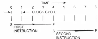
processor is inversely proportional to the product of clock cyc les per i nstruction (CPJ).I and the mach ine cyck time. From one generation of micro processors to the nt:xt, improvements i n both CPJ
and machine cycle t ime are requ ired in order to meet th<.:: performance goal. CPI depends on the microarchitcctutT as wel l as the m ix of instruc tions executed. Tht: minimum mach ine cycle time depends only on circu it and microarchitectural issues.
Improvements in CPI are achieved in parr by pipel ining and in part by adding cache memory
to
the die. As shown i n Figure 1 , pipe l i n i ng is defined as the simultaneous execution of two or more i nstructions; for example, the fi rst part of a two part i nstruction is cxt:cuted at the same time as the second part of the previous instruction. Simultane ons execution reduces the number of CPI; the resu lt is h igher performance at the expense of more circuitry.4 Adding on-ch ip cache memory also reduces the CPI. The microprocessor can qu ickly access i nstructions or data resident in i ts caches, rather than wait for this information to bt: trans mitted from on-board random-access memory (RA.\1) chips.Microprocessor Pe1jormcmce and Process Complexity in CMOS Technologies
NO PI PELINING
TIME 2 3 4 5 0
-I 1- CLOCK CYCLE
I
I
S
-F-IR-ST ______F
6 7 8
INSTRUCTION S --- F
SECOND INSTRUCTION NO PI PELINING: Second instruction does not start until the first instruction finishes. One instruction is executed every four cycles, so CPI = 4.
PIPELINING
0 -I
I
TIME
2 3 4 5
1- CLOCK CYCLE
I
S F -�
-R-ST ______ F
INSTRUCTION
6
s --- F SECOND
INSTRUCTION
7 8
s --- F THIRD
INSTRUCTION P I PELINING: Second instruction starts halfway through the execution of the first instruction. Third instruction starts halfway through the execution of the second. One instruction is executed every two cycles, so CPI = 2.
Note: I t takes more circuitry to implement a pipeline since instructions are executed simultaneously.
KEY:
S START F FINISH
Figure 1 Relationship between CPJ and Pipelining
As the m inimum feature size decreases, transistor density increases. Thus, for a given d ie size, a 0.75 -micrometer (J.Lm) minimum feature size tech nology
(CMOS-4)
can support four times as many transistors as a 1.5 -J.Lm technology(Ci'viOS-2).
In aclcli tion, advances in process technology lead to increases in t he size of the largest die that can be bu ilt with an acceptable manufacturing yield.Microprocessor designers take advantage of the extra transistors to increase the degree of pipe l ining and the size of caches. This reduces the
CPI,
which boosts the performance of the machine. Table 1 shows the difference between t wo genera tions of scaledCMOS
processes. The halving of the feature size has been augmented hy a larger d ie size and microarchitectural changes that i ncn:ase the SPECmark' performance by a factor of 4 . 8.Digital Technical journal Vol. 4 No. 2 Springi'J'J2
Generation-to-Generation Scaling
The pace of improvement i n microprocessor per formance inclicatecl by the REX520/NVAX compari son is ahead of the industry.!• Microprocessor perfo r mance has been doubl ing approximately every two years, and there is no evidence that this pace of change is slacken i ng. The shrinking of feature sizes with each new generation of CMOS
process technology and the increase in yieldable die sizes have enabled this rapid improvement in the performance of very large- scale integration
(VLSI)
chips.At the center of the reduction i n the feature sizes of
CMOS
processes is the miniaturization of theMOS
transistor. Over the past 15 years, a set of ru les, known as scal ing theory, has been developed toguide this process.7.H. 9
In the fu ndamental form of sca ling, ca l led con stant field scal ing, the transistor's physical parame ters and the power supply vol tage are kept proportional to the feature sizes to maintain the magnitude and the contours of the e lect ric fields within the transistor. Al l the dimensions of the tran sistor, e.g., length, width, gate dielectric thickness, and source/drain junction depths, and the power supply and threshold voltages are reduced by the scaling factor, [ 1/K (where K is greater than 1)] , while the eloping concentrat ions are increased by K. These rules are also extended, with some excep tions, to guide the miniaturization of the intercon nect. In practice, sca l ing theory is not fol lowed exactly, for reasons of both performance and stan dardization that are d iscussed below. Digital's implementation of scaling through four CMOS gen erations is shown in Table
2.
Improved Peiformance through Scaling The reduced feature sizes made possible by scal i ng have a major impact on node capacitance and, hence, the speed of the chip . The minimum cycle time of a microprocessor is i nversely proportional to the capacitances of the gates, sou rces, drains, and interconnect. The gate capacitance is inversely proportional to the thickness of the gate dielectric, and transistors with thinner gate d ielectrics have higher drive current. Since the minimum cycle time is a stronger fu nction of transistor drive current than gate dielectric capacitance, the trade-off shou ld be made in favor of a thinner gate dielectric. In Digita l 's family of
CMOS
processes, gate capaci tances have scaled with minimum feature size. [image:15.589.71.264.102.179.2]Semiconductor Technologies
Ta ble 1 Compa rison of Single Chip VAX Microprocessors
Cycle
M inimum Tape Time Chip
Feature Out Performance Cycles per (Nano- Size No. of
Process Size Chip Date SPECma rks* lnstructiont seconds) (Mils) Transistors
CMOS-2 1 .5 p.m REX520 Sep 87 8.5 1 1 .95 28 460X460 320,000 CMOS-4 0.75 p.m NVAX Nov 90 40.5 5.85 1 2 636X 574 1 ,300,000
Notes:
'These are combined i nteger and floating point SPECmarks run on a VAX 6000 Model 4 1 0 (REX520) and a VAX 6000 Model 610 (NVAX). 1 C PI depends not only on the CPU chip, but also on the memory subsystem and the particular program being executed. The CPI values
quoted here are a composite for the ten benchmark programs in the SPECmarks suite.
Table
2
Compa rison of Feature Sizes in CMOS Ge nerationsGate Dielectric Thickness (A} Minimum Featu re/Space (p.m}
Active area
Polysilicon/polycide Metal 1 with contact or via Metal 2 with via
Metal 3 with via
Minimum Featu re Size (p.m} Metal 1 contact
Metal 2 contact Metal 3 contact
Minimum Spacing (p.m) Metal 1 contact/polysilicon (in active area}
P+/N + active area
CMOS-1
300
4/2 2/2
4/2 5/2
2 2
2 8
From the 1 .5 -p.m minimum feature size of CMOS-2
technology to the 0.75 -p.m size of CMOS-4, the area
of the gates was scaled by a factor of four and the gate dielectric thickness was halved . The resu lt is a
twofold reduction in gate capacitance
(C = E0Ait).
The typical gate dielectric thickness in the 0.75-p.m
CMOS-4 process is
105 angstroms (A). Manufactura
bility and rel iability considerations have been the major factors determining the minimum gate dielectric thickness used for each generation.
As shown in Figure 2, the sources and drains of
n-channel metal-oxide semiconductor (NMOS) tran
sistors form N +/P diodes to the substrate. Since
the p-type doped substrate is held at a potential of
�s
(ground) and (during normal operation) thesources and drains are a lways at
�s or higher, these
diodes are always reverse biased and act as voltage dependent capacitors. The sources and drains of
p-channel metal-oxide semiconductor (PMOS)
tran-14
CMOS-2
225
3/1 .5 1 .5/1 .5 3/1 .5 3.75/1 .5
1 .5 1 .5
1 .5 6
CMOS-3
1 50
2/1 1 /1
2/1
2.5/1 4/6
1 1 4
1 4
CMOS-4
1 05
1 .5/0.75 0.75/0.75
1 .5/0.75
1 .875/0.75
3/4.5
0.75
0.75 3
0.75
3
sis tors form P+ IN diodes to the n-wells; the n-well
is held at vdd (power supply voltage).
The capacitance of a reverse-biased d iode is a function of its shape and size: there is both an area component and a perimeter component.
c[Q!al =
CJJ'l';l X Are
a+ cperimC!lT X Length_of_PerimeterSince the area scales with the square of the mini mum feature size and the perimeter scales directly with the feature size,
C101"1
scales by somewhat more than the minimum feature size: the exact amount depends on the shape of the source ordrain. For the NVAX microprocessor, which was
designed in CMOS-4, the area and perimeter compo
nents contribute about equally to
C101
.. 1 . In futuretechnology generations, the p erimeter component will tend to dominate.
In Digital's CMOS processes, metal interconnect
widths and spaces are scaled with the minimum
Microprocessor Performance and Process Complexity in
CMOS
Technologiesture size, but metal thicknesses and dielectric thick nesses are held constant to avoid three un desirable
Fi
gure 2 Diagram of NMOS and PMOS
TrausistorsShuwi11g
Gate,Source, and Drain for CMOS-4
CMOS-3
CMOS-4
effects. Sca l i ng the metal th ickness wou ld i ncrease the sheet resistance (lead ing to larger power supply voltage drops and
RC
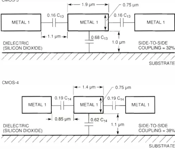
time constant de lays) and decrease the current-carrying capabil ity of the con ductor lines (from an electromigration viewpoint) . Scaling the in terconnect d ielectric th ickness wou ld increase the capacitance per unit area . Because the thicknesses of conductor l i nes and dielectric layers are not scaled, the aspect ratios of the spaces between the condu ctors and the contacts or v ias between i nterconnect l ayers increase. This makes fabrication more d ifficult.As with sources and d rains, interconnect capaci tance has both at1' area componen t, which sca les quadratical ly, and a perimetl'r component, which scales l inearly. Consequently, the total capacitance of i n tercon nect scales by somewhat more than the minimum feature size_ Because neither the i nter connect thickness nor the d ielectric thickness is scaled, the capacitance benveen adjacent conduc tor Jines increases. The result is an increased suscep tibility to cross-talk between adjacent bus signals. which is s hown in Figure :). In the NVAX micro processor, greater-than-minimum spaces were used on some critical buses to reduce cross -talk.
SUBSTRATE
[image:17.590.145.425.417.655.2]Note: C13 a d C 4 are the total capacitances lor the center line lor CMOS-3 and CMOS-4. respectively. Dimensions are typical.
Figure
3 Cross Section of Three
/Vlinimum -spacedMet
al I Lines Drawnto Scale for Ct\IJOS-3 and Ct\IJOS-4
Sem iconductor Technologies
The use of industry-standard power supply volt ages n::sults in a significant violation of constant field scaling rules. Nevertheless, power supply volt age is general ly held constant across two or more process generations [5.0 volts (V) in CMOS-I and
CMOS-2 and
3.3
V in CMOS-3 and CMOS-4] in order to maintain voltage compatibility with industry standard chips such as RAMs. However, a nonscaled power supply voltage presents formidable chal lenges for the design of reliable transistors.Developing CMOS for Microprocessors
The particular implementation of transistors, inter
connect, and special circuit elements in a c�os
process depends on the application. For Digit al's high-speed microprocessors, performance, as mea sured in SPECmarks, is crucial.'\ In addition to opti mizing the transistors for maximum drive current, performance in this appl ication can be improved by adding process features to provide denser on-chip cache static RAM (SRAM), interconnect with high current capabil ity, and precision resistors for impedance matching. As discussed above, per formance can also be improved by increasing the die size. By contrast, a major part of the effort in
designing a process for dynamic RAMs
(DRAM)
isdirected toward developing a very small, high capacitance memory element.
In addition to performance, the planned pro duction volume is an i mportant factor in
detin-ing a CMOS process. A process for low- to moderate volume, high-performance microprocessors differs from a process optimized for fast turnaround gate arrays or high-volume RAMs. In a high-volume prod uct, a great deal of effort is devoted to reducing the total nu mber of process steps. For example, com pensating blanket implants are often used to set the thresholds of the transistors to decrease the num ber of photolit hographic masking steps. This approach couples the parameters for the NMOS and PMOS transistors, making parameter adjustments more difficult and requiring more development effort.
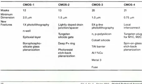
To produce h igh-performance microprocessors, Digital has developed many unique features for its
CMOS
technologies. Table 3I
ists the new technol ogy features that have been developed for each pro cess generation to meet increasingly demanding performance requirements. We begin our discus sion of the implementation of these features and the requ irements for rel iable circ u i t operation by addressing the issue of power dissipation in high speed microprocessors.Power Supply Voltage
It is well known that CMOS power dissipation is dominated by
C
X �,/ X
J, where C is the switched capacitance,vdd
is the power supply voltage, and f is the clock frequency. A reduction in1-drt
is an excel lent way to counteract the increase in power due toTable
3
Features Added by Generation for CMOS-1 to CMOS-4CMOS-11 CMOS-2 CMOS-3 CMOS-4
Masks 1 2 1 3 20 21
Minimum
Dimension 2.0 11-m 1 .5 11-m 1 .0 11-m 0.75 11-m
New
Features 1 X photolithography Lightly doped drain 5X g-line Local junction/spacer photolithography interconnect n-well
Tungsten n, p-polysilicon Tungsten plug
Epitaxial layer silicide gate for M1 C, M2C
Cobalt silicide
Borophospho- Deep P+ ring Spi n-on-glass
silicate glass TiN barrier etch-back
planarization Photoresist planarization
etch-back AI:1 %Cu
planarization
Metal 3
Fuse
[image:18.589.70.527.488.758.2]Microprocessor Performance and Process Complexity in
CMOSTeclmologies
the h igher frequencies and larger switched capaci tance (which results from the increase in d ie size). When developing the CMOS-3 process, we chose tO reduce the power supply vol tage from the industry norm of 5 v to the Joint Electronic Device Engi neering Council Ot:DEC) 3.3 V standard. 1"· 1 1
With the CMOS-4 process specified for 3.3-V power supply voltage, the NYA.."\ and the Alpha 2 1 064 microprocessors consume
16
watts (W) at100 megahertz (MHZ) and 27 W at 200 MHz, respec tivdy. If the supply volt age were 5.0 V, the power would scale by (5 V)2/(3.3 V)2
=
2.3. This increase in power dissipation would have greatly increased the complexity and cost of the chip packages.Significant changes tO the N,\'IOS and PMOS transis tors were necessary to optimize the process fo r operation at 3.3 V. The most visible parameter change was a lowering of the target threshold vo lt ages for the NMOS ancl PMOS transistors by about
I
0.4 1 v to 0.5 V and - 0. 5 V, respectively. To explain why this is necessary, we must consider the depen dence of both the nodal transition time (which is a good measure of circuit performance) ancl the tran sistor current:-; on1�111.
The time required to transi tion a signal node bet ween the power supply rails is proportional to the charge (Q) on the node ancl inversely p roport ional to the drain-to-source cur rent(111)
of the driving transistor. Since Qa t.-;1"
and , to first order,Ids a
"':,,/.
the time required to transi tion a node is inversely proportional to"':td·
How ever, when second-order effects are considered, the3.3-V technol ogy is of about the same performance as the corresponding 5 -V technology. The second order effects include the benefits from lowe ring the threshold voltages of the transistors in the 3.3-V pro cess and the compromises that would have to be made to the transistors in the 5-V process to make them reliable.
Ta ble 4 Orig ins of H igh Vo ltage Tra nsients
Power supply
Power supply tolerance On-chip power supply ringing due to package inductance
Booting above Vdd d ue to capacitive coupling Total
vds
(Volts)
3.30 0.1 65 0.1 75
0.66
4.30
Subtotal (Volts)
3.30 3.465 3.64
4.30
Digiln/ Teclmical journal Vol. 4 No. 2 Spring 1992
Hot Carrier Degradation
A CMOS transistor that is subjected to excessive volt ages becomes damaged over time by hot carriers. Hot carriers are h ighly energetic current carriers that result from the high electric fields in the tran sistor. To date, the N MOS transistor has been more susceptible to hot carrier degradation than the
PMOS transistor. Hot carrier dam age gradua l ly reduces the satu ration current fos!IT of the N MOS
transistor as the damage i ncreases over time. On chips with a nominal 3.3-V power supply, some transistors are subjected to sou rce-drain voltage transients as h igh as 4.3 v. Table 4 gives details of the origins of these h igh voltage transients.
Hot carrier rules fo r the CMOS-4 process are illus trated in Figure 4, which shows the three legal regions of device operation on a plot of
�s
(gate- to source voltage) versus"':ts
(drain-to-source voltage). Devices may operate in any, or all , of three regions:(1)
u nconditionally safe region,(2)
region subject to turn-on transient rule, and (3) extended safe region for "off" devices. Devices can spend up toVl
(J) >
UNCONDITIONALLY SAFE REGION
L
REGION SUBJECT4.5 V
1
-
--
--
/
-r----,-
---,
v
TO TURN-ON/
TRANSIENT RULE0.3 v
0.0
EXTENDED SAFE REGION FOR OFF DEVICES
/
/ l
3.6 v 4.3 v 4.5 v
Figure
4 CMOS-4Hot Carrier Rules
Comments
Nominal voltage
5% tolerance, includes ripple
From NVAX SPICE simulations. Half of peak-to-peak noise (Vdd-internal with respect to lf,5_internal)
Capacitive coupling to susceptible nodes is l i mited to < 20% by designers
Semiconductor Technologies
100
percent of the time in the safe region, no more than5
percent in the region subject to turn-on tran sient rule, and no more than10
percent in the "off" devices safety region.A wide variety of NVAX circu its wen: simu lated to determine what constraints shou ld be placed upon circuit design style in order to ensure that the
CMOS-4
hot carrier rules were not violated. A set of general circuit design constraints was devel oped, and a compu ter-aided design (CAD) tool was written to ensure that all the circuits on the NVA.X chip observed these constraints. The hot carrier CAD checks were run prior to fabrication, and circu its that violated the constraints were redesigned .Electromigration Considerations
If the average current density (
'"·mge)
through an aluminum conductor line is too high, the con ductor line is suscep tible to metal migration. This phenomenon occurs over time as the electron current fo rms voids at one site and deposits downstrea m. Eventually a short circuit or an open circuit develops, which resu lts in a circu it failure. Chip designers guard against electrom igration fail ure by ensuring tharJ,v�rag� for every conductor l ine on the chip is lower than the maximum allowed value.For a conductor l ine that is switched every cycle, the relationship between average current density, microprocessor cycle time
C�vcJe), l�trt•
and cross sectional area is given by!"nag� =
(C X �'" )
/C.Zrcle
X
Cross-Sectional Area) .
It is interesting to note the changes to
lav�rage
for a conductor I ine as a chip is shrunk from one generation to the next. The node capacitance,C,
decreases by slightly more than the sca ling factor;�"'
remains constant;�rck
reduces by the scal ing factor since the chip can now run faster; and the cross-sectional area decreases by the scaling factor. Consequently,;"'era�;�
increases by slightly less than rhe scal ing factor as the wiuth of the conductor l ine shrinks.lf.f1Vnage
now exceeds the maximum al lowed value, the circu i t must be redesigned . If there is enough space, .favera
ge
canbe reduced hy widening the conductor l i ne so that the cross-sectional area is increased. From this brief analysis, it is clear that it becomes more difficul t to observe the electromigrat ion l i mits as the technology scales-even when the metal thick ness is not scaled. As can be seen from the
.fwcragc
equation, reducing�td
from5.0
V in CMOS-2 to :).3 V1 8
i n CMOS-3 helped t o counteract the effect o f scal ing onJ,vcragc·
Scaling the interconnect and dealing with electro migration issues are some of the most formidable challenges that must be faced as feature sizes con tinue to decrease in the next decade.
Substrate Contact
As mentioned earlier, the substrate m ust be con nected to the
�-
of the chip through a low i mpedance path to prevent any rise in voltage. If ' the substrate voltage rise is severe, NMOS source/drain diodes wil l conduct, and if sufficient charge is injected, the chip may latch-up. Latch-up is a destructive mechanism involving the parasitic bipolar transistors formed by the CMOS process. The process, circu its, and
V:s
substrate contact are designed to prevent latch-up from occurring.The usual industry substrate connection method depends on a path through bond wires and the package to connect between in ternal V55 and the substrate. To ensure a good substrate contact, Digital's CMOS technologies incorporate a deep P + implant (DPI) around the edge o f the d i e to connect the
V55
metal on the d ie surface to the low-resistance substrate . The implant creates a low-resistance path through the ?-epi taxial layer in which the NMOS and PMOS transistors are formed.The DPI is a low-induct ance path when com pared to the standard method that connects the substrate through the package. The additional area enclosed by the path through the boncl wires and package impl ies greater inductance, which is unde sirable for high-frequency signals. The DPI path between V . .\.\ and substrate has low inductance because i t is made directly on-chip.
Technology-limited Gate Dielectric
Thickness
As stated above, maximizing the current that a tran sistor can supply at a given
�'"
is of uppermost importance for circui t performance. Sca l ing the transistor gate length, gate dielectric thickness, and threshold voltage improves the d rive current. The transistor gate length is constrained by the mini mum polysilicon line-width feature; the minimum threshold voltage is set by the kakage current al lowed when the transistor is turned off. However, scal ing does not establish a fixed n:lationship between feature size and gate d ielectric thickness; scal ing only determines the change from one gener ation to the next.Microprocessor Performance and Process Complexity in CMOS Technologies
Figure 5 shows how the saturation currents for both NMOS and PMOS transistors in CMOS-4 depend on the gate dielectric thickness. The dielectric thickness range plotted spans applications from microprocessors to SRAMs. Both curves are only slightly sublinear; thinning the gate dielectric provides almost a one-to-one return in transistor saturation current. In high-performance micro processor applications, rel iability and manufac turability considerations determine the extent to which the gate dielectric thickness can be reduced. Digital's C\10S technologies have consistently used thinner gate dielectrics than industry norms.
o<( lf) :":
X 0
f-@J
0.
rn � ...._ � �
4
3
2
[image:21.588.58.266.260.520.2]7
Figure
5
NMOS TRANSISTOR
1 0
Normalized Drive Current as a Function of Gate Dielectric Thickness for CMOS-4
Silicided Source/drain and Gate
1 1
The basic gate material for an MOS transistor is highly doped polysil icon. The sheet resistivity of this material in the CMOS-1 process was 40 ohms per square. For CMOS-2, the RC time constant delay associated with this sheet resistance would have created nonuniform turn-on of wide, fast-switching output transistors. A tungsten silicide layer was added to the polysilicon to form a polycide. The sandwich structure reduced the sheet resistance of the gate material to 3 ohms per square.
Changes to the transistor process for CMOS-3
technology, which were continued into CMOs-4,
Digital Techtticaljournal Vol. 4 No. 2 Spring1992
required development of a new silicided gate pro cess. The new process, known as sal icide for self aligned silicide, forms the silicide on the gate and on the source/drain regions after a l l the required transistor implants have been completed. This reduces the sheet resistance of the source/drain regions by more than an order of magnitude and allows them to be considered for use in local sig nal rou ting. The reduced sheet resistance, how ever, does l it tle to improve the current drive of the transistor; for a typical CMOS-4 NMOS transistor,
MINIMOS simu lations show that the use of sil icided source/drain regions improves the saturation cur rent by only 0.6 percent. 12
Precision Resistor
Although transistors are the dominant element in logic design, a resistor is sometimes needed, for example, to match the impedance of an output driver with the impedance of a board-level trans mission line that it drives. MOS transistors make poor controlled impedance drivers because they change impedance as a function of drain voltage. One method of controlling the impedance of a driver is to use a diffusion resistor as the dominant element, as shown in Figure 6. The MOS transistors are sized such that their on-state resistance is much lower than that of the resistor. Therefore, if the transmission l ine impedance is 50 ohms, the resis tor plus transistor impedance can be sized to match that value with little influence from the variations in transistor impedance.
Resistors are constructed from nonsilicidecl dif fusion to meet tolerance requirements that would not be possible with a silicicled version. Because a silicidecl resistor has lower sheet resistance, it is much longer and narrower than a nonsil icided
DRIVER
Figure
6
BOARD
CHIP
J,
TRANSMISSION LINE
RECEIVER
Precision Resistor Use in Impedance Jll/atching