Simulation and Performance Assessment of OLED
for Energy Efficient Communication Display
Applications
1
Priya Chaudhary, 2Ashok Sirohi, 3Manju Mathur
1
M.tech Scholar, 2Ph.D, 3Assistant Professor, Digital Communication, Rajasthan College of Engineering for Women, Jaipur, India
Abstract:OLEDs, known as organic light-emitting diodes, are a kind of technology with emitting light flat developed by inserting
thin film of organic compound between two conductors, for example, a carbon dioxide on the principle of electro phosphorescence for converting electric energy into light energy in a very effective way. OLEDs technology, which is convenient for collecting more attraction of end users, is bright, lighter, thinner, more energy efficient and offers a higher contrast than liquid crystal displays. It deals with wide- angle OLEDs watches, faster response time, high contrast ratio and more saturation. The OLEDs is one of the bright lighting technologies, capable of delivering more efficient and better lighting compared to the incandescent bulbs of this fluorescent lamp. The primary goal of the work is to simulate and analyse the performance of OLEDs based on different structures and different layers, to analysis the performance of OLED by varying active layer material and to compare performance of the various OLEDs structures based on performance parameters.
Index Terms: Organic Light emitting diode (OLEDs), Multilayer, Energy Efficient, Display, Communication
I. INTRODUCTION
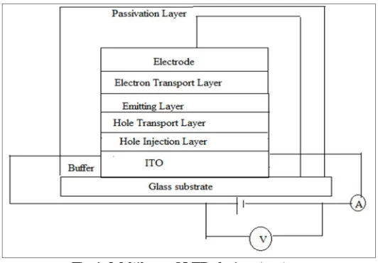
Fig 1: Multilayer OLED device structure
The following is a physical and mathematical description
µ ( ) = µ exp ( − . + . − , | |)
µ ( ) = µ exp (− . + . − . √∣ ∣
where,
DELTAEN.PFMOB, DELTAEP.PFMOB = Activation energy at zero electric field for electrons and holes respectively. µn0 (E) = Field dependent mobility
µn0= Zero field mobility E = Electric field
BETAN.PFMOB, BETAP.PFMOB = Electron and hole Poole-Frenkel factor respectively.
To forecast the results of OLEDs under proper boundary conditions, The Langevin recombination rate coefficient is given by
( , , ) = LANGEVIN [µ ( ) + µ ( )]
є є
where,
R = rate of recombination
e= the charge of electron which is 1.6 × 10⁻¹⁹,
μe = Mobility of electron,
μh =Mobility of hole,
ε= Permittivity of material,
εo= Permittivity of air which is 8.85×10⁻¹² F/cm.
If the logical parameter KOSTER is specified on the MODEL statement, the Langevin rate is given by:
( , , ) = LANGEVIN (µ µ )
є є
The Langevin recombination rate is given by:
, = ( , , )( −
The fundamental equations consist of Poisson’s equation, the continuity equations and the transport equations as follows
Poisson’s Equation shows relation between variations in the electrostatic potential and local charge density of electrons and holes. It is mathematically described by the following relation [7].
= local space charge density
= local permittivity of the semiconductor (F/cm) = ionized donor density(cm-3)
p= hole density (cm-3)
n = electron density (cm-3) and
= ionized acceptor density(cm-3).
The reference potential is still considered to be the intrinsic Fermi potential for ATLAS simulation. To accountfor the trapped charge, Poisson’s equations are modified by adding an additional term QT, representing trapped charge:
. () = - q (p-n+N -N ) - QT
WhereQT= q (N +N ).Here N and N =ionizeddensity of donor like traps and ionized density ofaccepter like traps respectively
For electrons and holes, the continuity equationsare defined as follows[7].
The area of the device is 108 µm2. Indium tin oxide (ITO) is used as anode for hole injection due to its high work function and transparency. The cathode used here is of LiF/Al as electron injection. The two-layer device contained of a stack of 1-Naphdata and Alq3 each, whereas the three-layer device consisted of a stack of 1-Naphdata, -NPD, and Alq3. The organic layers were inserted
between ITO and LiF/Al electrodes.
II. DEVICESTRUCTURE
[image:3.612.175.440.443.723.2]The proposed structures comprise of three layers stacked over one another; these layers are to be specific cathode layer, natural layer and anode layer and every one of these layers are mounted over a substrate which is utilized to help OLED. Cathode layer is stored on the highest point of dynamic layer and made up of having work 3.8 eV and it fill in as electron injection layer. Second layer is natural layer which is kept on anode and it separates as recombination layer where on use of voltage electrons from the cathode and openings from the anode recombines and in this manner prompts excitons arrangement, some of which rot radiative to the ground state by unconstrained light discharge. Proposed structure comprises of various natural layers for example (1-Naphdata)/(α -NPD)/Alq3 Bottom most layer for example anode segment normally utilized is indium tin oxide ITO. This material is straightforward to noticeable light and is adequately conductor and has a high work (5.0 eV) which advances injection of openings into the HOMO dimension of the natural layer.
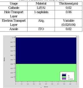
Table I. Parameters for bilayer oled
Usage Material Thickness(µm) Cathode LiF/Al 0.02 Hole Transport
Layer
1-naphdata 0.06
Electron Transport Layer
Alq3 Variable
(0.02/0.04)
Anode ITO 0.02
There are many layers in a multilayer OLED, but only one additional luminescent layer is introduced here, as shown in Fig.2. The EML layer used here is Alq3. An M1L layer is introduced in the middle of the OLED layer. In this layer, electron-hole pairs are recombined to produce photons [13]. By introducing various fluorescent and phosphorescent small molecules, the band gap energy between the HOMO and LUMO levels can be controlled [14].The simulated structure of Device 3 is shown in Fig 3.
Fig.3. Simulated structure of Device 3 (Multilayer OLED)
To improve the efficiency of OLEDs the Langevin recombination model is used to predict the results under proper boundary conditions. This model visualizes the conduction due to field enhanced thermal excitation. Increase in biasing voltage improved the recombination rate.
III. SIMULATIONANDRESULTS
Efficiency can be increased by adding EML (emitter layer). After manufacturing a single layer, the two-layer and three-layer OLED L-V characteristics of device structure 3 are superior to those of device 2. Due to the higher recombination rate, the three-layer structure has Low anode current but high luminescence power [10]. Higher recombination rate because the organic/organic interface reduces the energy barrier height and enhances carrier injection. The current depends on voltage and temperature. The current density should also follow The number of layers increases and increases. The rate of recombination depends on the mobility of the holes, electrons and the dielectric constant of the materials used. The recombination of carriers is the most important phenomenon in OLEDs because the light emission is completely dependent on it. By adding more layers of high dielectric constant, the recombination rate can be increased. The probability of recombination due to electrons and holes increases the likelihood of exciton formation. Therefore, the number of photons increases and the emission of light increases.
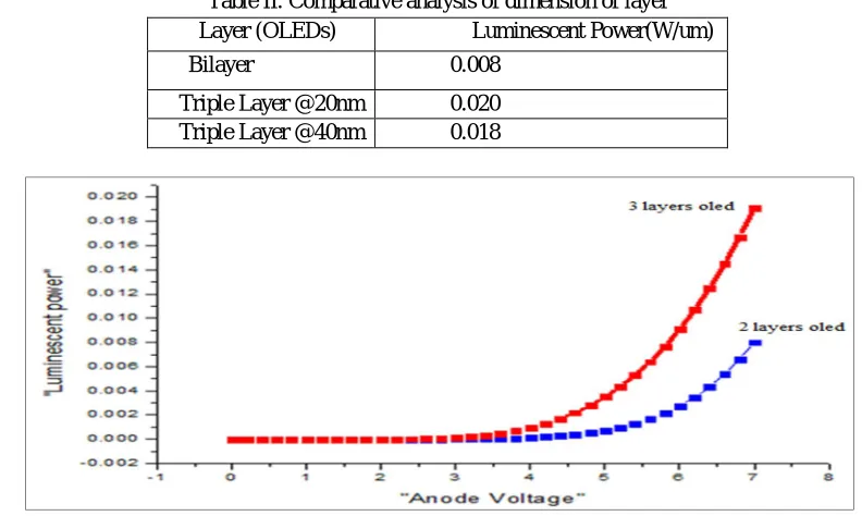
Table II. Comparative analysis of dimension of layer Layer (OLEDs) Luminescent Power(W/um) Bilayer 0.008
[image:4.612.105.501.487.724.2]Triple Layer @20nm 0.020 Triple Layer @40nm 0.018
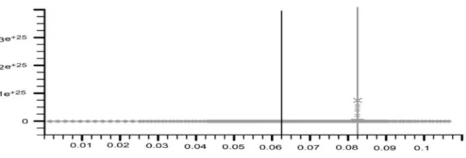
Fig 3: Comparative Analysis of Recombination rate of Device structures
In a two-layer OLED, an organic layer is interposed between the hole transport layer and the electron transport layer. ETL is added to the metal cathode and is responsible for transporting electrons from the cathode to the emissive layer (EML). The ETL used here is Alq3. The hole transport layer (HTL) used herein is 1-naphdata. The purpose of this layer is to transport holes from the luminescent layer to the anode. This must be the analog structure of the p-type semiconductor device 2 as shown.
IV. CONCLUSION
The general correlation of execution parameters communicates that the execution of proposed structure demonstrates more vitality proficient and have preferable quantum productivity over 2 layer oled. Execution assessment has been done on premise of four execution parameters which are anode current, luminescent power, effectiveness and Langevin recombination rate. It is obvious that the estimation of luminescent power of proposed multilayer oled is superior to that of structure 1. It is likewise clear that the expansion of luminescent power is conceivable because of higher estimation of Langevin recombination rate. It very well may be presumed that in spite of the estimation of anode current is higher in two layer organic LED. Because of quick increment in estimation of Langevin recombination rate the exhibitions of three layer structure have higher proficiency and higher luminescent power when contrasted with structure 1.Proposed gadget turns out to be reasonable possibility for application in foldable and adaptable hardware and advanced presentation applications because of polymer structure and better glowing effectiveness.
REFERENCES
[1] Klaus Müllen, UllrichScherf, Organic Light Emitting Devices: Synthesis, Properties and Applications, Wiley-VCH, 1st edition (2006).
[2] C. W. Tang and S. A. VanSlyke, Appl. Phys. Lett. 51, 913 (1987).
[3] R. H. Friend, R. W. Gymer, A. B. Holmes, J. H. Burroughes, R. N. Marks, C. Taliani, D. D. C. Bradley, D. A. Dos Santos, J. L. Bredas, M. Logdlund, and W.
R. Salaneck, Nature (London) 397, 121 (1999).
[4] M.A Baldo, D.F O’Brien, Y. You, A. Shoustikov, S.Sibley, M.E. Thompson, and S.R, Forrest, Nature 395, 151 (1998).
[5] S.-J, Su, Y.Takahashi, T.chiba, T.Takeda, and J.kido, advance functional material 19,1260(2009)
[6] K.R choudhury, J.Lee, N. chopra, A. Gupta, X Jiang, F.Amy, and F. So advanced functional Material 19, 491 (2009)
[7] M. G. Helander, Z-B.Wang, M.T.Grenier, Z-W.Liu, J. Qiu and Z-H. Lu, Adv. Mater. 22, 2037(2010).
[8] Z.W. Liu, M.G.Helander, Z.B. Wang, and Z.H.Lu, Appl. Phys. Lett.94, 113305(2009).
[9] P. K. Sandhu, S. Singla, “OLED – An imminent technology’’, International Journal of Engineering Research and General Science, vol. 3, pp. 611-616, 2015.
[10] Chih-Lung Lin, Tsung-Ting Tsai, and Yung-Chih Chen,” A Novel Voltage-Feedback Pixel Circuit forAMOLEDDisplays”, Journal Of Display Technology,
vol. 4, pp. 54-60, March 2008.
[11] Y. L Chang, Z. H. Lu, “White organic light-emitting diodes for solid-state lighting”, Journal of Display Technology, vol. 9, pp. 459-468, June 2013.
[12] K. Y. Chen et. al., “enhancement and saturation phenomena on luminous current and power efficiencies or organic light-emitting devices by attaching micro
lens array films”, Journal of Display Technology, vol. 7, pp. 242-249, 2011.
[13] P. K. Sandhu, S. Singla, “OLED – An imminent technology’’, Int. J. of Engineering Research and General Science, vol. 3, pp. 611-616, 2015.
[14] G. S. Samal et al. “Improved efficiency in fluorescent blue organic light emitting diode with a carrier confining structure”, Journal of Organic Electronics, vol
10, pp. 1207-1208, 2009.
[15] Gill, W.D., "Drift Mobilities in Amorphous Charge-Transfer Complexes of Trinitrofluorenone and Poly-n-vinylcarbazole", J. Appl. Phys. Vol. 55, No. 12, 1972, p. 5033.
[16] Sivaji Reddy, V & Das, K & Ray, Samit & Dhar, Achintya. (2018). Characteristics of MEH-PPV thin films on ITO electrode for organic light emitting diodes.
[17] Yousefi, Mohammad & Fallahzadeh, Ali & Saghaei, Jaber & Davoudi Darareh, Mahdi. (2016). Fabrication of flexible ITO-free OLED using vapor-treated PEDOT:PSS thin film as anode. Journal of Display Technology. PP. 1-1. 10.1109/JDT.2016.2624341.
[18] R. Chowdhury, M. R. Haq, S. Paul and M. S. U. Chowdhury, "Numerical analysis of performance improvement of modified ITO based organic light emitting
diode," 2015 International Conference on Advances in Electrical Engineering (ICAEE), Dhaka, 2015, pp. 348-351.
[19] G. R. Chaji and A. Nathan, "Parallel Addressing Scheme for Voltage-Programmed Active-Matrix OLED Displays," in IEEE Transactions on Electron Devices,
vol. 54, no. 5, pp. 1095-1100, May 2007.
[20] Jiyoun, S & Seokki, Y & Sons, M & Park, Chinho. (2006). Fabrication of red, green, and blue organic light-emitting diodes using m-MTDATA as a common